EP1655760A2 - Plasmaanzeigevorrichtung - Google Patents
Plasmaanzeigevorrichtung Download PDFInfo
- Publication number
- EP1655760A2 EP1655760A2 EP05256904A EP05256904A EP1655760A2 EP 1655760 A2 EP1655760 A2 EP 1655760A2 EP 05256904 A EP05256904 A EP 05256904A EP 05256904 A EP05256904 A EP 05256904A EP 1655760 A2 EP1655760 A2 EP 1655760A2
- Authority
- EP
- European Patent Office
- Prior art keywords
- discharge cell
- display apparatus
- plasma display
- scan
- central portion
- Prior art date
- Legal status (The legal status is an assumption and is not a legal conclusion. Google has not performed a legal analysis and makes no representation as to the accuracy of the status listed.)
- Withdrawn
Links
- 239000000758 substrate Substances 0.000 claims abstract description 66
- 230000004888 barrier function Effects 0.000 claims abstract description 49
- 238000000034 method Methods 0.000 claims description 12
- 230000009977 dual effect Effects 0.000 description 7
- OAICVXFJPJFONN-UHFFFAOYSA-N Phosphorus Chemical compound [P] OAICVXFJPJFONN-UHFFFAOYSA-N 0.000 description 5
- 239000007789 gas Substances 0.000 description 5
- 230000003071 parasitic effect Effects 0.000 description 5
- 230000001681 protective effect Effects 0.000 description 4
- 239000011261 inert gas Substances 0.000 description 3
- 230000015556 catabolic process Effects 0.000 description 2
- 238000010276 construction Methods 0.000 description 2
- 238000006731 degradation reaction Methods 0.000 description 2
- 230000001788 irregular Effects 0.000 description 2
- 239000000395 magnesium oxide Substances 0.000 description 2
- CPLXHLVBOLITMK-UHFFFAOYSA-N magnesium oxide Inorganic materials [Mg]=O CPLXHLVBOLITMK-UHFFFAOYSA-N 0.000 description 2
- AXZKOIWUVFPNLO-UHFFFAOYSA-N magnesium;oxygen(2-) Chemical compound [O-2].[Mg+2] AXZKOIWUVFPNLO-UHFFFAOYSA-N 0.000 description 2
- 230000002459 sustained effect Effects 0.000 description 2
- VYZAMTAEIAYCRO-UHFFFAOYSA-N Chromium Chemical compound [Cr] VYZAMTAEIAYCRO-UHFFFAOYSA-N 0.000 description 1
- 229910052786 argon Inorganic materials 0.000 description 1
- 238000010304 firing Methods 0.000 description 1
- 229910052734 helium Inorganic materials 0.000 description 1
- AMGQUBHHOARCQH-UHFFFAOYSA-N indium;oxotin Chemical compound [In].[Sn]=O AMGQUBHHOARCQH-UHFFFAOYSA-N 0.000 description 1
- 229910052743 krypton Inorganic materials 0.000 description 1
- 229910052751 metal Inorganic materials 0.000 description 1
- 239000002184 metal Substances 0.000 description 1
- 239000000203 mixture Substances 0.000 description 1
- 238000012986 modification Methods 0.000 description 1
- 230000004048 modification Effects 0.000 description 1
- 229910052754 neon Inorganic materials 0.000 description 1
- 238000004544 sputter deposition Methods 0.000 description 1
- 229910052724 xenon Inorganic materials 0.000 description 1
- YVTHLONGBIQYBO-UHFFFAOYSA-N zinc indium(3+) oxygen(2-) Chemical compound [O--].[Zn++].[In+3] YVTHLONGBIQYBO-UHFFFAOYSA-N 0.000 description 1
- TYHJXGDMRRJCRY-UHFFFAOYSA-N zinc indium(3+) oxygen(2-) tin(4+) Chemical compound [O-2].[Zn+2].[Sn+4].[In+3] TYHJXGDMRRJCRY-UHFFFAOYSA-N 0.000 description 1
Images


Classifications
-
- H—ELECTRICITY
- H01—ELECTRIC ELEMENTS
- H01J—ELECTRIC DISCHARGE TUBES OR DISCHARGE LAMPS
- H01J11/00—Gas-filled discharge tubes with alternating current induction of the discharge, e.g. alternating current plasma display panels [AC-PDP]; Gas-filled discharge tubes without any main electrode inside the vessel; Gas-filled discharge tubes with at least one main electrode outside the vessel
- H01J11/20—Constructional details
-
- H—ELECTRICITY
- H01—ELECTRIC ELEMENTS
- H01J—ELECTRIC DISCHARGE TUBES OR DISCHARGE LAMPS
- H01J11/00—Gas-filled discharge tubes with alternating current induction of the discharge, e.g. alternating current plasma display panels [AC-PDP]; Gas-filled discharge tubes without any main electrode inside the vessel; Gas-filled discharge tubes with at least one main electrode outside the vessel
- H01J11/10—AC-PDPs with at least one main electrode being out of contact with the plasma
- H01J11/12—AC-PDPs with at least one main electrode being out of contact with the plasma with main electrodes provided on both sides of the discharge space
-
- H—ELECTRICITY
- H01—ELECTRIC ELEMENTS
- H01J—ELECTRIC DISCHARGE TUBES OR DISCHARGE LAMPS
- H01J11/00—Gas-filled discharge tubes with alternating current induction of the discharge, e.g. alternating current plasma display panels [AC-PDP]; Gas-filled discharge tubes without any main electrode inside the vessel; Gas-filled discharge tubes with at least one main electrode outside the vessel
- H01J11/20—Constructional details
- H01J11/34—Vessels, containers or parts thereof, e.g. substrates
- H01J11/36—Spacers, barriers, ribs, partitions or the like
-
- H—ELECTRICITY
- H01—ELECTRIC ELEMENTS
- H01J—ELECTRIC DISCHARGE TUBES OR DISCHARGE LAMPS
- H01J2211/00—Plasma display panels with alternate current induction of the discharge, e.g. AC-PDPs
- H01J2211/20—Constructional details
- H01J2211/34—Vessels, containers or parts thereof, e.g. substrates
- H01J2211/36—Spacers, barriers, ribs, partitions or the like
- H01J2211/361—Spacers, barriers, ribs, partitions or the like characterized by the shape
- H01J2211/365—Pattern of the spacers
Definitions
- the present invention relates to a plasma display apparatus.
- a plasma display apparatus capable of reducing panel capacitance by improving a shape of discharge cells so as to be driven according to a single scan method.
- a plasma display apparatus is an apparatus in which discharge cells are formed between a lower substrate with barrier ribs formed thereon and an upper substrate facing the lower substrate, and when an inert gas inside each discharge cell is discharged by a high frequency voltage, vacuum ultraviolet rays are generated to illuminate phosphor to thereby allow displaying of images.
- FIG. 1 is a plan view of electrodes formed in a general plasma display apparatus
- FIG. 2 is a sectional view showing a discharge cell of the general plasma display apparatus.
- discharge cells are formed by a plurality of barrier ribs 24 separating a discharge space on a lower substrate 18 facing an upper substrate 10.
- An address electrode 12X is formed on the lower substrate 18, and a scan electrode 12Y and a sustain electrode 12Z are formed as a pair on the upper substrate 10.
- the address electrode 12X crosses the other electrodes, and in this respect, the upper substrate 10 in FIG. 1 is shown as having been rotated by 90° for the sake of explanation.
- a dielectric layer 22 for accumulating wall charges is formed on the lower substrate 18 with the address electrode 12 formed thereon.
- Barrier ribs 24 are formed on the dielectric layer 22 to define a discharge space therebetween and prevent a leakage of ultraviolet rays and visible light generated by a discharge to an adjacent discharge cell.
- Phosphor 26 is coated on the surface of the dielectric layer 22 and on the surface of the barrier ribs 24. Because an inert gas is injected into the discharge space, the phosphor 26 is excited by the ultraviolet rays generated during a gas discharge to generate one of red, green and blue visible light.
- the scan electrode 12Y and the sustain electrode 12Z formed on the upper substrate 10 comprise a transparent electrode 12a and a bus electrode 12b, respectively, and cross the address electrode 12X.
- a dielectric layer 14 and a protective film 16 are formed to cover the scan electrode 12Y and the sustain electrode 12Z.
- the discharge cell with such a structure is selected by a facing discharge formed between the address electrode 12X and the scan electrode 12Y, and a discharge is sustained by a surface discharge between the scan electrode 12Y and the sustain electrode 12Z, to thus emit visible light.
- the scan electrode 12Y and the sustain electrode 12Z comprise the transparent electrode 12a and the bus electrode 12b having the smaller width than the transparent electrode 12a and formed on one edge portion of the transparent electrode 12a, respectively.
- the related art plasma display apparatus has the following problem. That is, as the resolution of the panel is increasingly improved and the panel is being enlarged in size, time for scanning the address electrodes is lengthened. In addition, as the length of each electrode and the number of electrode lines increase in line with the enlargement of the panel, panel parasitic capacitance is also increased to make the plasma display apparatus consume more power
- a dual scan type plasma display apparatus comprises two address drivers 31 and 32 for driving address electrodes in a dual scan manner, a scan driver 40 for driving scan electrodes, and a sustain driver 50 for driving sustain electrodes.
- the first address driver 31 applies a data signal to drive a first address electrode group (X1 1 to X1 m ) of a display panel 60 to output an image on an upper screen
- the second address driver 32 applies a data signal to drive a second address electrode group (X2 1 to X2 m ) of the display panel 60 to output an image on a lower screen.
- the scan driver 40 can divide the scan electrodes (Y 1 to Y n ) into two groups (Y 1 to Y n/2 and Y n/2+1 to Y n ) and sequentially applies a scan pulse to electrodes of each group simultaneously, to thereby reduce an address period to 1/2.
- the dual scan type plasma display apparatus is, however, disadvantageous in that more data driver integrated circuits are required to be mounted in each of the address drivers 31 and 32 compared with a single scan type plasma display apparatus, resulting in an increase in the cost, and power consumption is also increased due to the parasitic capacitance of the panel.
- Embodiments of the present invention seek to alleviate such problems of the related art, and therefore, attempt to provide a plasma display apparatus capable of reducing panel capacitance by improving a shape of discharge cells so as to be driven according to a single scan method.
- a plasma display apparatus comprising a plurality of upper electrodes, a plurality of lower electrodes and barrier ribs.
- the plurality of upper electrodes are formed on an upper substrate.
- the plurality of lower electrodes are formed on a lower substrate facing the upper substrate, crossing the upper electrodes.
- the barrier ribs separate a plurality of discharge cells formed between the upper substrate and the lower substrate. The discharge cell is formed such that a horizontal width of one of an upper and a lower portion thereof is different from that of a central portion thereof.
- the discharge cell can have rounded corner portions.
- the discharge cell can be formed such that the horizontal width narrows as it goes from the central portion to the upper or lower portion.
- the upper or lower horizontal width of the discharge cell may be 90% or greater but smaller than 100% of the horizontal width of the central portion of the discharge cell.
- the upper electrode may comprise a scan electrode, and can be driven by a single scan driving method in which a scan pulse is applied to each of a plurality of scan electrodes formed on a display region of the upper substrate at each different time, respectively.
- a plasma display apparatus comprising a plurality of upper electrodes, a plurality of lower electrodes and barrier ribs.
- the plurality of upper electrodes are formed on an upper substrate.
- the plurality of lower electrodes are formed on a lower substrate facing the upper substrate, crossing the upper electrodes.
- the barrier ribs separate a plurality of discharge cells formed between the upper substrate and the lower substrate. The discharge cell is formed such that a vertical width of one of a left and a right portion thereof is different from that of a central portion thereof.
- a plasma display apparatus comprising a plurality of scan electrodes, barrier ribs and a scan driver.
- the plurality of scan electrodes are formed on an upper substrate.
- the barrier ribs are formed on a lower substrate facing an upper substrate.
- the scan driver applies a scan pulse to the scan electrodes.
- Discharge cells separated by the barrier ribs are formed such that a horizontal width or a vertical width of an outer portion thereof is different from that of a central portion thereof, and the scan driver applies the scan pulse to the plurality of scan electrodes at each different time, respectively.
- a plasma display apparatus comprises a plurality of upper electrodes formed on an upper substrate, a plurality of lower electrodes formed on a lower substrate facing the upper substrate and crossing the upper electrodes, and barrier ribs separating a plurality of discharge cells formed between the upper substrate and the lower substrate.
- the discharge cells a horizontal width of at least one of an upper portion and a lower portion of the discharge cell is different from that of a central portion of the discharge cell.
- the plurality of upper electrodes are formed on the upper substrate, on which a dielectric layer is stacked to cover the upper electrodes.
- a protective film is formed on the surface of the dielectric layer.
- a lower electrode is formed on the lower substrate which faces the upper substrate to form a discharge therebetween, and a dielectric layer is stacked to cover the lower electrode.
- barrier ribs 70a and 70b separating the discharge cells 60 are formed on the dielectric layer.
- the barrier ribs 70a and 70b comprise the horizontal barrier rib 70a and the vertical barrier rib 70b, constituting a closed type barrier rib form.
- the lower electrode comprises an address electrode.
- the lower electrode is formed in a direction that it crosses the upper electrode.
- the upper electrode comprises a scan electrode and a sustain electrode, and each electrode comprises a transparent electrode and a metallic bus electrode having a width smaller than that of the transparent electrode and formed on one edge portion of the transparent electrode.
- the transparent electrode includes a metal such as an indium tin oxide (ITO), an indium zinc oxide (IZO) or an indium tin zinc oxide (ITZO), and the metallic bus electrode typically made of chrome (Cr) is formed on the transparent electrode and serves to reduce a voltage drop by the transparent electrode having high resistance.
- the dielectric layer is formed to cover the electrodes formed on the upper and lower substrates.
- the protective film includes magnesium oxide (MgO), prevents the dielectric layer from being damaged by sputtering generated when a plasma discharge occurs, and increases the efficiency of emission of secondary electrons. Accordingly, the dielectric layer and the protective film can serve to lower a discharge firing voltage.
- MgO magnesium oxide
- the barrier ribs 70a and 70b form the discharge space together with the upper and lower substrates and prevent a leakage of vacuum ultraviolet rays generated according to a gas discharge to an adjacent discharge cell.
- the discharge space may be filled with an inert gas such as He, Ne, Ar, Xe, Kr, etc., for a gas discharge, a discharge gas of a mixture thereof, or an excimer gas that can generate ultraviolet rays according to the discharge.
- a phosphor layer is coated on the side surface of the barrier ribs 70a and 70b or on the surface of the dielectric layer within the discharge space and excited by the vacuum ultraviolet rays (VUV) generated when the plasma discharge occurs, to emit one of red (R), green (G) and blue (B) visible light.
- VUV vacuum ultraviolet rays
- the horizontal barrier rib 70a is formed to be parallel to the scan electrode and the sustain electrode on the lower substrate.
- the vertical barrier rib 70b is formed to be parallel to the address electrode on the lower substrate.
- a unit discharge cell separated by the horizontal and vertical barrier ribs 70a and 70b will be described in detail based on its shape viewed from the upper substrate.
- the unit discharge cell has a horizontal width and a vertical width, and in this case, a horizontal width of at least one of an upper portion or a lower portion of the discharge cell is smaller than that of a central portion of the discharge cell. Namely, the portion of the discharge cell contacting with the horizontal barrier rib is narrower than the central portion of the central portion (e.g., the distance between the horizontal barrier ribs) of the discharge cell.
- the width of the portion where the horizontal barrier rib and the horizontal rib cross can be extended, and thus, capacitance according to the barrier ribs can be reduced.
- FIG. 5 illustrates first and fourth embodiments and FIGs. 6 to 9 illustrate various application examples of the discharge cell in accordance with second and fifth embodiments.
- FIG. 5 shows the first embodiment in which a discharge cell has symmetrical upper and lower portions. That is, in the plasma display apparatus in accordance with the first embodiment, at least one of the upper portion and lower portion of the discharge cell has rounded corners.
- both the upper portion and the lower portion of the discharge cell have the symmetrically rounded corners
- the width of the barrier rib at both corner portions can be lengthened to make the barrier rib thick.
- the horizontal width (d1) of the upper portion or the lower portion of the discharge cell can be smaller than the horizontal width (b1) of the central portion of the discharge cell.
- FIGS. 6 to 9 show various application examples of the discharge cell with symmetrical upper and lower portions in accordance with the second embodiment.
- a plasma display apparatus in accordance with the second embodiment has a structure in that the discharge cell is formed such that its horizontal width narrows as it goes from the central portion thereof to the upper portion or the lower portion thereof.
- the discharge cell sustains the same horizontal width (b2) of the central portion from the central portion to a certain portion, and becomes gradually narrow from the certain portion to reach a certain size (d2) of the horizontal width at an outermost upper portion or lower portion.
- the horizontal width (b3) of the discharge cell is reduced starting from the central portion and gradually reduced as it goes to the upper portion or the lower portion of the discharge cell to finally have a certain size (d3) of the horizontal width at the outermost upper or lower portion of the discharge cell.
- the horizontal width (b4) of the central portion of the discharge cell is sustained from the central portion up to a certain portion, and becomes gradually narrow as it goes from the certain portion to the upper portion or the lower portion to end in convergence of the left and right vertical barrier ribs of the discharge cell.
- the width (b5) of the discharge cell is reduced starting from the central portion toward the upper portion or the lower portion of the discharge cell to end in convergence of the left and right vertical barrier ribs of the discharge cell.
- the second embodiment may include a case where the horizontal width of the discharge cell is not linearly reduced but reduced by several stages as it goes to the upper portion or the lower portion, making the corner portions of the discharge cell have an irregular shape.
- the first and second embodiments may include a case where the discharge cell has such asymmetrical shape that the horizontal width of the upper portion of the discharge cell is not the same as that of the lower portion of the discharge cell.
- a plasma display apparatus in accordance with a third embodiment has a structure in that the horizontal width of the upper portion or the lower portion of the discharge cell is 90% or greater but smaller than 100% of that of the central portion of the discharge cell. That is, with reference to FIGs. 5 to 7, the horizontal widths (d1, d2 and d3) of the upper portion or the lower portion of the discharge cell may be 90% or greater or smaller than 100% of that of the horizontal widths (b1, b2 and b3) of the central portion of the discharge cell.
- the horizontal width of the upper portion of the discharge cell is smaller than 90% of the horizontal width of the central portion in order to reduce the area of the discharge cell and increase the width of the barrier ribs, capacitance of the panel could be lowered but since the area of the discharge cell is reduced, the area of the phosphor layer coated inside the discharge cell is also reduced to cause a problem that the luminance of the panel is reduced.
- the horizontal width of the upper portion of the discharge cell is smaller than 90% of the horizontal width of the central portion, picture quality degradation occurs such that it would be perceived by a user.
- the plasma display apparatus comprises a plurality of upper electrodes formed on an upper substrate, a plurality of lower electrodes formed on a lower substrate facing the upper substrate and crossing the upper electrodes, and barrier ribs separating a plurality of discharge cells formed between the upper substrate and the lower substrate.
- the discharge cells a vertical width of at least one of a left portion and a right portion of the discharge cell is different from that of a central portion of the discharge cell.
- FIG. 5 shows the fourth embodiment in which the discharge cell has symmetrical left and right portions. That is, in the plasma display apparatus in accordance with the fourth embodiment, at least one of the left portion and the right portion of the discharge cell has rounded corners. Though it is shown that both the left portion and the right portion of the discharge cell have symmetrically rounded corners, it is also possible for only one side of the left portion and right portion of the discharge cell to have rounded corners. Namely, since the left and right corner portions of the discharge cell have the round shape with a certain radius of curvature, the width of the barrier rib at both corner portions can be lengthened to make the barrier rib thick. With such rounded corners, the vertical width (c1) of the left portion or the right portion of the discharge cell is smaller than the vertical width (a1 ) of the central portion of the discharge cell.
- FIGs. 6 to 9 show various application examples of the discharge cell with symmetrical left and right portions in accordance with the fifth embodiment.
- a plasma display apparatus in accordance with the fifth embodiment has a structure in that the discharge cell is formed such that its horizontal width narrows as it goes from the central portion thereof to the left portion or the right portion thereof.
- the discharge cell sustains the same horizontal width (a2) of the central portion from the central portion to a certain portion, and becomes gradually narrow from the certain portion to reach a certain size (c2) of the vertical width at an outermost left portion or right portion.
- the discharge cell sustains the same vertical width (a3) of the central portion from the central portion to the certain portion, and becomes gradually narrow as it goes to the left portion or to the right portion of the discharge cell to end in convergence of the upper and lower horizontal barrier ribs of the discharge cell.
- the vertical width (a4) of the discharge cell is reduced starting from the central portion gradually as it goes to the left portion or the right portion of the discharge cell to finally have a certain size (c4) of the vertical width at the left or right portion of the discharge cell.
- the width (a5) of the discharge cell is reduced starting from the central portion gradually as it goes to the left portion or the right portion of the discharge cell to end in convergence of the upper and lower horizontal barrier ribs of the discharge cell.
- the second embodiment may include a case where the vertical width of the discharge cell is not linearly reduced but reduced by several stages as it goes to the left portion or the right portion, making the corner portions of the discharge cell have an irregular shape.
- the fourth and fifth embodiments may include a case where the discharge cell has such an asymmetrical shape that the vertical width of the left portion of the discharge cell is not the same as that of the right portion of the discharge cell.
- a plasma display apparatus in accordance with a sixth embodiment has a structure in that the vertical width of the left portion or the right portion of the discharge cell is 80% or greater but smaller than 100% of that of the central portion of the discharge cell. That is, with reference to FIGs. 5, 6 and 8, the vertical widths (c1, c2 and c4) of the upper portion or the lower portion of the discharge cell may be 80% or greater or smaller than 100% of that of the vertical widths (a1, a2 and a4) of the central portion of the discharge cell.
- the vertical width of the upper portion of the discharge cell is smaller than 90% of the horizontal width of the central portion, picture quality degradation occurs such that it would be perceived by the user. That is, as described above in the first to sixth embodiments, in the plasma display apparatus, by forming the discharge cell separated by the barrier ribs such that its outer horizontal width is 90% or greater but smaller than 100% of the central horizontal width, or by forming the discharge cell such that its outer vertical width is 80% greater but smaller than 100% of the central vertical width, a value of the parasitic capacitance generated by the address electrode can be reduced.
- the plasma display apparatus comprises the plurality of scan electrodes formed on the upper substrate, the barrier ribs formed on the lower substrate facing the upper substrate, and the scan driver for applying the scan pulse to the scan electrodes.
- the discharge cells separated by the barrier ribs are formed such that the horizontal width or vertical width of an outer portion of the discharge cell is different from the horizontal width or the vertical width of the central portion of the discharge cell, and the scan driver applies the scan pulse to the plurality of scan electrodes at each different time, respectively, according to the single scan method.
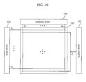
- FIG. 10 illustrates an exemplary construction of a single scan type plasma display apparatus Since the data driver integrated circuit consumes less power, the plasma display apparatus having the above-described structure of the barrier ribs can be driven according to the single scan driving method by using drivers 110, 120 and 130 as shown in FIG. 10.
- the plasma display apparatus comprises a scan driver 110 for driving scan electrodes Y1 ⁇ Yn of the panel 100, a sustain driver 120 for driving a sustain electrode (Z) of the panel 100, and an address driver 130 for driving address electrodes X1 ⁇ Xn of the panel 100.
- the scan driver 110 initializes the entire wall charges of the panel 100 by using a lamp waveform during a reset period under the control of a timing controller (not shown). Next, the scan driver 110 sequentially applies a negative scan pulse to the scan electrodes Y1 ⁇ Yn during an address period to scan signals applied to the address electrode.
- FIG. 11 illustrates the scan pulse applied to each of scan electrodes Y1 ⁇ Yn during the address period.
- the scan driver 110 employs the single scan method to apply the scan pulse to the plurality of scan electrodes at each different time, respectively.
- the number of scan electrode lines formed on the display region exceeds 480.
- the number of the scan electrode lines on the display region refers to the scan electrodes lines positioned only at the portion of a screen where image information is actually outputted.
- alternative arrangements having fewer lines are possible
- the plasma display apparatus in accordance is driven according to the single scan method, and the discharge cell separated by the barrier ribs is formed such that the horizontal width or vertical width of the outer portion of the discharge cell is different from that of the central portion of the discharge cell.
- the discharge cell separated by the barrier ribs is formed such that the horizontal width or vertical width of the outer portions of the discharge cell is smaller than that of the central portion of the discharge cell.
- this is not essential.
- embodiments of the plasma display apparatus have the following advantages.
- the panel is so large as to have the number of scan electrode lines of 480 or more, since the discharge cell separated by the barrier ribs is formed such that the horizontal width or the vertical width of the outer portions of the discharge cell is smaller than the horizontal or the vertical width of the central portion of the discharge cell to thereby reduce the parasitic capacitance of the panel, it can be sufficiently driven one address driver.
- the present invention can be favorably applicable to a panel of XGA class, namely, which has 768 or more scan lines and generally requires more data drivers because it cannot be driven by the only data driver formed at the upper side or at the lower side of the panel. That is, by adopting the present invention, such a large panel having 768 or more scan lines can be driven by only one data driver formed either at the upper side or at the lower side of the panel.
- the region where the 768 scan lines are formed refers to a display region.
Landscapes
- Physics & Mathematics (AREA)
- Engineering & Computer Science (AREA)
- Plasma & Fusion (AREA)
- Gas-Filled Discharge Tubes (AREA)
Applications Claiming Priority (1)
| Application Number | Priority Date | Filing Date | Title |
|---|---|---|---|
| KR1020040090964A KR100638211B1 (ko) | 2004-11-09 | 2004-11-09 | 플라즈마 디스플레이 패널 |
Publications (2)
| Publication Number | Publication Date |
|---|---|
| EP1655760A2 true EP1655760A2 (de) | 2006-05-10 |
| EP1655760A3 EP1655760A3 (de) | 2009-01-21 |
Family
ID=35695051
Family Applications (1)
| Application Number | Title | Priority Date | Filing Date |
|---|---|---|---|
| EP05256904A Withdrawn EP1655760A3 (de) | 2004-11-09 | 2005-11-08 | Plasmaanzeigevorrichtung |
Country Status (4)
| Country | Link |
|---|---|
| US (1) | US20060097649A1 (de) |
| EP (1) | EP1655760A3 (de) |
| KR (1) | KR100638211B1 (de) |
| CN (1) | CN1773662B (de) |
Families Citing this family (2)
| Publication number | Priority date | Publication date | Assignee | Title |
|---|---|---|---|---|
| US7482752B2 (en) * | 2005-01-20 | 2009-01-27 | Lg Electronics Inc. | Plasma display panel with electrode pairs at display and non-display regions, each pair having a different separation gap on each region |
| JP4728170B2 (ja) * | 2006-05-26 | 2011-07-20 | 三菱電機株式会社 | 半導体デバイスおよびアクティブマトリクス型表示装置 |
Citations (1)
| Publication number | Priority date | Publication date | Assignee | Title |
|---|---|---|---|---|
| US20040135508A1 (en) | 2003-01-02 | 2004-07-15 | Jae-Ik Kwon | Plasma display panel |
Family Cites Families (18)
| Publication number | Priority date | Publication date | Assignee | Title |
|---|---|---|---|---|
| JPH09213215A (ja) * | 1996-01-30 | 1997-08-15 | Nippon Sheet Glass Co Ltd | プラズマディスプレイ装置及びプラズマディスプレイ装置用ガラス基板の製造方法 |
| EP1017083A1 (de) * | 1998-12-21 | 2000-07-05 | Thomson Plasma | Plasma-Anzeigetafel bestehend aus einer porösen Struktur |
| JP2001110325A (ja) * | 1999-10-13 | 2001-04-20 | Mitsubishi Electric Corp | ガス放電表示パネル及びその製造方法 |
| JP2001266751A (ja) | 2000-03-17 | 2001-09-28 | Hitachi Ltd | メタル隔壁およびこれを用いたプラズマデイスプレイパネル |
| JP3409784B2 (ja) * | 2000-10-25 | 2003-05-26 | 松下電器産業株式会社 | プラズマディスプレイ表示装置およびその製造方法 |
| JP3788927B2 (ja) * | 2000-11-28 | 2006-06-21 | 三菱電機株式会社 | プラズマディスプレイパネル及びプラズマディスプレイ装置 |
| US6495967B2 (en) * | 2001-04-06 | 2002-12-17 | Chunghwa Picture Tubes, Ltd. | Discharge cells between barrier walls of alternating current discharge type plasma display panel |
| TW564457B (en) * | 2001-06-12 | 2003-12-01 | Matsushita Electric Industrial Co Ltd | Plasma display device and driving method for the plasma display device |
| JP3640622B2 (ja) * | 2001-06-19 | 2005-04-20 | 富士通日立プラズマディスプレイ株式会社 | プラズマディスプレイパネルの駆動方法 |
| JP2003132805A (ja) * | 2001-08-14 | 2003-05-09 | Sony Corp | プラズマ表示装置 |
| KR100447120B1 (ko) * | 2001-12-28 | 2004-09-04 | 엘지전자 주식회사 | 플라즈마 디스플레이 패널의 구동방법 및 장치 |
| JP2003208848A (ja) * | 2002-01-16 | 2003-07-25 | Mitsubishi Electric Corp | 表示装置 |
| JP2003338246A (ja) * | 2002-05-21 | 2003-11-28 | Sony Corp | プラズマ表示装置およびその製造方法 |
| JP2004164885A (ja) * | 2002-11-11 | 2004-06-10 | Matsushita Electric Ind Co Ltd | プラズマディスプレイパネルおよびその製造方法 |
| US7538491B2 (en) * | 2002-12-27 | 2009-05-26 | Lg Electronics Inc. | Plasma display panel having differently shaped transparent electrodes |
| US7315122B2 (en) * | 2003-01-02 | 2008-01-01 | Samsung Sdi Co., Ltd. | Plasma display panel |
| KR100502910B1 (ko) * | 2003-01-22 | 2005-07-21 | 삼성에스디아이 주식회사 | 델타 화소 배열 구조를 갖는 플라즈마 디스플레이 패널 |
| KR100508949B1 (ko) * | 2003-09-04 | 2005-08-17 | 삼성에스디아이 주식회사 | 플라즈마 디스플레이 패널 |
-
2004
- 2004-11-09 KR KR1020040090964A patent/KR100638211B1/ko not_active Expired - Fee Related
-
2005
- 2005-11-08 EP EP05256904A patent/EP1655760A3/de not_active Withdrawn
- 2005-11-08 US US11/268,736 patent/US20060097649A1/en not_active Abandoned
- 2005-11-09 CN CN200510120250XA patent/CN1773662B/zh not_active Expired - Fee Related
Patent Citations (1)
| Publication number | Priority date | Publication date | Assignee | Title |
|---|---|---|---|---|
| US20040135508A1 (en) | 2003-01-02 | 2004-07-15 | Jae-Ik Kwon | Plasma display panel |
Also Published As
| Publication number | Publication date |
|---|---|
| CN1773662A (zh) | 2006-05-17 |
| US20060097649A1 (en) | 2006-05-11 |
| KR20060042429A (ko) | 2006-05-15 |
| EP1655760A3 (de) | 2009-01-21 |
| CN1773662B (zh) | 2010-11-17 |
| KR100638211B1 (ko) | 2006-10-26 |
Similar Documents
| Publication | Publication Date | Title |
|---|---|---|
| KR100272418B1 (ko) | Ac형 플라즈마 디스플레이 판넬 및 구동방법 | |
| JPH1167100A (ja) | Ac型プラズマディスプレイパネル | |
| JP3641240B2 (ja) | プラズマディスプレイパネルとその駆動方法 | |
| CN101635243A (zh) | 等离子体显示面板 | |
| EP1655760A2 (de) | Plasmaanzeigevorrichtung | |
| JPH08212933A (ja) | 面放電型プラズマディスプレイパネル及びその駆動方法 | |
| US20050218805A1 (en) | Plasma display panel and plasma display | |
| CN101501810B (zh) | 等离子体显示设备 | |
| JP2001068030A (ja) | 3電極型acプラズマディスプレイパネル | |
| KR100710819B1 (ko) | 교류 타입 플라즈마 디스플레이 패널의 스캔 구동 방법 | |
| KR20030026777A (ko) | 플라즈마 디스플레이 패널 | |
| WO2007105481A1 (ja) | プラズマディスプレイ装置 | |
| KR100625541B1 (ko) | 플라즈마 표시 패널 구동 방법 및 장치 | |
| KR100351465B1 (ko) | 플라즈마 디스플레이 패널 및 그 구동방법 | |
| KR100680696B1 (ko) | 플라즈마 표시 패널 구동 방법 및 장치 | |
| KR100366946B1 (ko) | 플라즈마 디스플레이 패널 | |
| JP2002366098A (ja) | プラズマディスプレイパネルの駆動方法 | |
| KR100817559B1 (ko) | 플라즈마 디스플레이 패널 | |
| KR100762248B1 (ko) | 플라즈마 디스플레이 패널 | |
| KR20060065130A (ko) | 플라즈마 디스플레이 패널 | |
| WO2007105480A1 (ja) | プラズマディスプレイ装置 | |
| WO2007102329A1 (ja) | プラズマディスプレイ装置 | |
| WO2009096639A1 (en) | Plasma display apparatus and method of driving | |
| JP2004309764A (ja) | ガス放電表示装置の駆動方法 | |
| KR20060067420A (ko) | 다전극 구조의 플라즈마 디스플레이 패널 및 플라즈마디스플레이 장치 |
Legal Events
| Date | Code | Title | Description |
|---|---|---|---|
| PUAI | Public reference made under article 153(3) epc to a published international application that has entered the european phase |
Free format text: ORIGINAL CODE: 0009012 |
|
| 17P | Request for examination filed |
Effective date: 20051116 |
|
| AK | Designated contracting states |
Kind code of ref document: A2 Designated state(s): AT BE BG CH CY CZ DE DK EE ES FI FR GB GR HU IE IS IT LI LT LU LV MC NL PL PT RO SE SI SK TR |
|
| AX | Request for extension of the european patent |
Extension state: AL BA HR MK YU |
|
| RIC1 | Information provided on ipc code assigned before grant |
Ipc: H01J 17/16 20060101ALI20080201BHEP Ipc: H01J 17/49 20060101AFI20060206BHEP |
|
| PUAL | Search report despatched |
Free format text: ORIGINAL CODE: 0009013 |
|
| AK | Designated contracting states |
Kind code of ref document: A3 Designated state(s): AT BE BG CH CY CZ DE DK EE ES FI FR GB GR HU IE IS IT LI LT LU LV MC NL PL PT RO SE SI SK TR |
|
| AX | Request for extension of the european patent |
Extension state: AL BA HR MK YU |
|
| AKX | Designation fees paid |
Designated state(s): DE FR GB NL |
|
| 17Q | First examination report despatched |
Effective date: 20090914 |
|
| STAA | Information on the status of an ep patent application or granted ep patent |
Free format text: STATUS: THE APPLICATION IS DEEMED TO BE WITHDRAWN |
|
| 18D | Application deemed to be withdrawn |
Effective date: 20100407 |