EP1655720A2 - Affichage électronique et méthode de fabrication de celui-ci - Google Patents
Affichage électronique et méthode de fabrication de celui-ci Download PDFInfo
- Publication number
- EP1655720A2 EP1655720A2 EP05255654A EP05255654A EP1655720A2 EP 1655720 A2 EP1655720 A2 EP 1655720A2 EP 05255654 A EP05255654 A EP 05255654A EP 05255654 A EP05255654 A EP 05255654A EP 1655720 A2 EP1655720 A2 EP 1655720A2
- Authority
- EP
- European Patent Office
- Prior art keywords
- backplate
- layer
- electronic
- electronic display
- array
- Prior art date
- Legal status (The legal status is an assumption and is not a legal conclusion. Google has not performed a legal analysis and makes no representation as to the accuracy of the status listed.)
- Withdrawn
Links
Images


Classifications
-
- G—PHYSICS
- G09—EDUCATION; CRYPTOGRAPHY; DISPLAY; ADVERTISING; SEALS
- G09G—ARRANGEMENTS OR CIRCUITS FOR CONTROL OF INDICATING DEVICES USING STATIC MEANS TO PRESENT VARIABLE INFORMATION
- G09G3/00—Control arrangements or circuits, of interest only in connection with visual indicators other than cathode-ray tubes
- G09G3/20—Control arrangements or circuits, of interest only in connection with visual indicators other than cathode-ray tubes for presentation of an assembly of a number of characters, e.g. a page, by composing the assembly by combination of individual elements arranged in a matrix no fixed position being assigned to or needed to be assigned to the individual characters or partial characters
- G09G3/34—Control arrangements or circuits, of interest only in connection with visual indicators other than cathode-ray tubes for presentation of an assembly of a number of characters, e.g. a page, by composing the assembly by combination of individual elements arranged in a matrix no fixed position being assigned to or needed to be assigned to the individual characters or partial characters by control of light from an independent source
- G09G3/3433—Control arrangements or circuits, of interest only in connection with visual indicators other than cathode-ray tubes for presentation of an assembly of a number of characters, e.g. a page, by composing the assembly by combination of individual elements arranged in a matrix no fixed position being assigned to or needed to be assigned to the individual characters or partial characters by control of light from an independent source using light modulating elements actuated by an electric field and being other than liquid crystal devices and electrochromic devices
- G09G3/3466—Control arrangements or circuits, of interest only in connection with visual indicators other than cathode-ray tubes for presentation of an assembly of a number of characters, e.g. a page, by composing the assembly by combination of individual elements arranged in a matrix no fixed position being assigned to or needed to be assigned to the individual characters or partial characters by control of light from an independent source using light modulating elements actuated by an electric field and being other than liquid crystal devices and electrochromic devices based on interferometric effect
-
- G—PHYSICS
- G02—OPTICS
- G02F—OPTICAL DEVICES OR ARRANGEMENTS FOR THE CONTROL OF LIGHT BY MODIFICATION OF THE OPTICAL PROPERTIES OF THE MEDIA OF THE ELEMENTS INVOLVED THEREIN; NON-LINEAR OPTICS; FREQUENCY-CHANGING OF LIGHT; OPTICAL LOGIC ELEMENTS; OPTICAL ANALOGUE/DIGITAL CONVERTERS
- G02F1/00—Devices or arrangements for the control of the intensity, colour, phase, polarisation or direction of light arriving from an independent light source, e.g. switching, gating or modulating; Non-linear optics
- G02F1/01—Devices or arrangements for the control of the intensity, colour, phase, polarisation or direction of light arriving from an independent light source, e.g. switching, gating or modulating; Non-linear optics for the control of the intensity, phase, polarisation or colour
- G02F1/21—Devices or arrangements for the control of the intensity, colour, phase, polarisation or direction of light arriving from an independent light source, e.g. switching, gating or modulating; Non-linear optics for the control of the intensity, phase, polarisation or colour by interference
-
- G—PHYSICS
- G02—OPTICS
- G02B—OPTICAL ELEMENTS, SYSTEMS OR APPARATUS
- G02B26/00—Optical devices or arrangements for the control of light using movable or deformable optical elements
- G02B26/001—Optical devices or arrangements for the control of light using movable or deformable optical elements based on interference in an adjustable optical cavity
-
- G—PHYSICS
- G09—EDUCATION; CRYPTOGRAPHY; DISPLAY; ADVERTISING; SEALS
- G09G—ARRANGEMENTS OR CIRCUITS FOR CONTROL OF INDICATING DEVICES USING STATIC MEANS TO PRESENT VARIABLE INFORMATION
- G09G2300/00—Aspects of the constitution of display devices
- G09G2300/04—Structural and physical details of display devices
-
- Y—GENERAL TAGGING OF NEW TECHNOLOGICAL DEVELOPMENTS; GENERAL TAGGING OF CROSS-SECTIONAL TECHNOLOGIES SPANNING OVER SEVERAL SECTIONS OF THE IPC; TECHNICAL SUBJECTS COVERED BY FORMER USPC CROSS-REFERENCE ART COLLECTIONS [XRACs] AND DIGESTS
- Y10—TECHNICAL SUBJECTS COVERED BY FORMER USPC
- Y10T—TECHNICAL SUBJECTS COVERED BY FORMER US CLASSIFICATION
- Y10T29/00—Metal working
- Y10T29/49—Method of mechanical manufacture
- Y10T29/49002—Electrical device making
- Y10T29/49117—Conductor or circuit manufacturing
- Y10T29/49124—On flat or curved insulated base, e.g., printed circuit, etc.
- Y10T29/49155—Manufacturing circuit on or in base
Definitions
- the field of the invention relates to microelectromechanical systems (MEMS). More specifically, the field of the invention relates to interferometric modulator based displays.
- MEMS microelectromechanical systems
- Display devices such as LCDs generally require electronic controlling circuitry located exterior to a protective package surrounding the display element.
- an LCD comprises two sheets of glass surrounding a liquid crystal element.
- Controlling an LCD typically requires circuitry external to the package formed by the two sheets of glass.
- Positioning such controlling circuitry exterior to this protective package necessarily increases either the footprint or the height of the device.
- MEMS microelectromechanical systems
- These MEMS can include micro mechanical elements, actuators, and electronics.
- Micromechanical elements may be created using deposition, etching, and or other micromachining processes that etch away parts of substrates and/or deposited material layers or that add layers to form electrical and electromechanical devices.
- An interferometric modulator may comprise a pair of conductive plates, one or both of which may be transparent and/or reflective in whole or part and capable of relative motion upon application of an appropriate electrical signal.
- One plate may comprise a stationary layer deposited on a substrate, the other plate may comprise a metallic membrane separated from the stationary layer by an air gap.
- Such devices have a wide range of applications, and it would be beneficial in the art to utilize and/or modify the characteristics of these types of devices so that their features can be exploited in improving existing products and creating new products that have not yet been developed.
- One embodiment of the invention is a display, wherein the display includes: a transparent substrate; an array of interferometric modulators comprising reflective elements that are configured to reflect light through said transparent substrate; a backplane comprising a first surface proximal to the array of interferometric modulators and comprising electronic circuitry fabricated on said first surface of the backplane, wherein the electronic circuitry is configured to control the movement of the reflective elements; and a plurality of electrical connections providing electronic communication between the electronic circuitry on the backplane and the array of interferometric modulators.
- Yet another embodiment of the invention is a method of fabricating a display, comprising: providing a transparent substrate comprising an array of interferometric modulators on a first surface of the transparent substrate, wherein said modulators comprise reflective elements; providing a backplate having a first surface; forming electronic circuitry on the first surface of the backplate, wherein the electronic circuitry is configured to control the state said reflective elements; and positioning the transparent substrate and the backplate such that the first surface of the transparent substrate is located proximal the first surface of the backplate and the electronic circuitry is placed in electrical connection with the array of interferometric modulators.
- Still another embodiment of the invention is a display made by the method of: providing a transparent substrate comprising an array of interferometric modulators on a first surface of the transparent substrate, wherein said modulators comprise reflective elements; providing a backplate having a first surface; forming electronic circuitry on the first surface of the backplate, wherein the electronic circuitry is configured to control the state said reflective elements; and positioning the transparent substrate and the backplate such that the first surface of the transparent substrate is located proximal the first surface of the backplate and the electronic circuitry is placed in electrical connection with the array of interferometric modulators.
- An embodiment of the invention is an interferometric modulator-based display wherein the backplate contains electronic circuitry fabricated on the interior side of the backplate.
- This electronic circuitry is capable, among other things, of controlling the state of the array of interferometric modulators. This is useful, for example, in order to provide the display driver circuit within the display package.
- the fabrication of the driver chip within the display package, and on the interior side of the backplate advantageously permits greater flexibility in the design of the electronic circuitry.
- such fabrication advantageously permits optimal use of space within the display, permitting the creation of a device which may be thinner and/or have a smaller footprint than prior devices.
- the fabrication of the electronic circuitry, rather than the use of existing driver chips, may also result in significant cost savings.
- the following detailed description is directed to certain specific embodiments of the invention. However, the invention can be embodied in a multitude of different ways. In this description, reference is made to the drawings wherein like parts are designated with like numerals throughout. As will be apparent from the following description, the invention may be implemented in any device that is configured to display an image, whether in motion (e.g., video) or stationary (e.g., still image), and whether textual or pictorial.
- motion e.g., video
- stationary e.g., still image
- the invention may be implemented in or associated with a variety of electronic devices such as, but not limited to, mobile telephones, wireless devices, personal data assistants (PDAs), hand-held or portable computers, GPS receivers/navigators, cameras, MP3 players, camcorders, game consoles, wrist watches, clocks, calculators, television monitors, flat panel displays, computer monitors, auto displays (e.g., odometer display, etc.), cockpit controls and/or displays, display of camera views (e.g., display of a rear view camera in a vehicle), electronic photographs, electronic billboards or signs, projectors, architectural structures, packaging, and aesthetic structures (e.g., display of images on a piece of jewelry).
- MEMS devices of similar structure to those described herein can also be used in non-display applications such as in electronic switching devices.
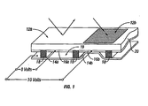
- interferometric modulator display embodiment comprising an interferometric MEMS display element is illustrated in Figure 1.
- the pixels are in either a bright or dark state.
- the display element In the bright ("on” or “open") state, the display element reflects a large portion of incident visible light to a user.
- the dark (“off” or “closed”) state When in the dark (“off” or “closed”) state, the display element reflects little incident visible light to the user.
- the light reflectance properties of the "on” and "off” states may be reversed.
- MEMS pixels can be configured to reflect predominantly at selected colors, allowing for a color display in addition to black and white.
- Figure 1 is an isometric view depicting two adjacent pixels in a series of pixels of a visual display, wherein each pixel comprises a MEMS interferometric modulator.
- an interferometric modulator display comprises a row/column array of these interferometric modulators.
- Each interferometric modulator includes a pair of reflective layers positioned at a variable and controllable distance from each other to form a resonant optical cavity with at least one variable dimension.
- one of the reflective layers may be moved between two positions. In the first position, referred to herein as the released state, the movable layer is positioned at a relatively large distance from a fixed partially reflective layer.
- the movable layer In the second position, the movable layer is positioned more closely adjacent to the partially reflective layer. Incident light that reflects from the two layers interferes constructively or destructively depending on the position of the movable reflective layer, producing either an overall reflective or non-reflective state for each pixel.
- the depicted portion of the pixel array in Figure 1 includes two adjacent interferometric modulators 12a and 12b.
- a movable and highly reflective layer 14a is illustrated in a released position at a predetermined distance from a fixed partially reflective layer 16a.
- the movable highly reflective layer 14b is illustrated in an actuated position adjacent to the fixed partially reflective layer 16b.
- the fixed layers 16a, 16b are electrically conductive, partially transparent and partially reflective, and may be fabricated, for example, by depositing one or more layers each of chromium and indium-tin-oxide onto a transparent substrate 20. The layers are patterned into parallel strips, and may form row electrodes in a display device as described further below.
- the movable layers 14a, 14b may be formed as a series of parallel strips of a deposited metal layer or layers (orthogonal to the row electrodes 16a, 16b) deposited on top of posts 18 and an intervening sacrificial material deposited between the posts 18. When the sacrificial material is etched away, the deformable metal layers are separated from the fixed metal layers by a defined air gap 19.
- a highly conductive and reflective material such as aluminum may be used for the deformable layers, and these strips may form column electrodes in a display device.
- the cavity 19 remains between the layers 14a, 16a and the deformable layer is in a mechanically relaxed state as illustrated by the pixel 12a in Figure 1.
- a potential difference is applied to a selected row and column
- the capacitor formed at the intersection of the row and column electrodes at the corresponding pixel becomes charged, and electrostatic forces pull the electrodes together.
- the movable layer is deformed and is forced against the fixed layer (a dielectric material which is not illustrated in this Figure may be deposited on the fixed layer to prevent shorting and control the separation distance) as illustrated by the pixel 12b on the right in Figure 1.
- the behavior is the same regardless of the polarity of the applied potential difference. In this way, row/column actuation that can control the reflective vs. non-reflective pixel states is analogous in many ways to that used in conventional LCD and other display technologies.
- Figures 2 through 5 illustrate one exemplary process and system for using an array of interferometric modulators in a display application.
- Figure 2 is a system block diagram illustrating one embodiment of an electronic device that may incorporate aspects of the invention.
- the electronic device includes a processor 21 which may be any general purpose single- or multi-chip microprocessor such as an ARM, Pentium® , Pentium II® , Pentium III® , Pentium IV® , Pentium® Pro, an 8051, a MIPS® , a Power PC® , an ALPHA® , or any special purpose microprocessor such as a digital signal processor, microcontroller, or a programmable gate array.
- a processor 21 which may be any general purpose single- or multi-chip microprocessor such as an ARM, Pentium® , Pentium II® , Pentium III® , Pentium IV® , Pentium® Pro, an 8051, a MIPS® , a Power PC® , an ALPHA
- the processor 21 may be configured to execute one or more software modules.
- the processor may be configured to execute one or more software applications, including a web browser, a telephone application, an email program, or any other software application.
- the processor 21 is also configured to communicate with an array controller 22.
- the array controller 22 includes a row driver circuit 24 and a column driver circuit 26 that provide signals to a pixel array 30.
- the cross section of the array illustrated in Figure 1 is shown by the lines 1-1 in Figure 2.
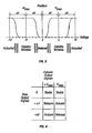
- the row/column actuation protocol may take advantage of a hysteresis property of these devices illustrated in Figure 3. It may require, for example, a 10 volt potential difference to cause a movable layer to deform from the released state to the actuated state. However, when the voltage is reduced from that value, the movable layer maintains its state as the voltage drops back below 10 volts.
- the movable layer does not release completely until the voltage drops below 2 volts.
- the row/column actuation protocol can be designed such that during row strobing, pixels in the strobed row that are to be actuated are exposed to a voltage difference of about 10 volts, and pixels that are to be released are exposed to a voltage difference of close to zero volts.
- each pixel sees a potential difference within the "stability window" of 3-7 volts in this example.
- This feature makes the pixel design illustrated in Figure 1 stable under the same applied voltage conditions in either an actuated or released pre-existing state. Since each pixel of the interferometric modulator, whether in the actuated or released state, is essentially a capacitor formed by the fixed and moving reflective layers, this stable state can be held at a voltage within the hysteresis window with almost no power dissipation. Essentially no current flows into the pixel if the applied potential is fixed.
- a display frame may be created by asserting the set of column electrodes in accordance with the desired set of actuated pixels in the first row.
- a row pulse is then applied to the row 1 electrode, actuating the pixels corresponding to the asserted column lines.
- the asserted set of column electrodes is then changed to correspond to the desired set of actuated pixels in the second row.
- a pulse is then applied to the row 2 electrode, actuating the appropriate pixels in row 2 in accordance with the asserted column electrodes.
- the row 1 pixels are unaffected by the row 2 pulse, and remain in the state they were set to during the row 1 pulse. This may be repeated for the entire series of rows in a sequential fashion to produce the frame.
- the frames are refreshed and/or updated with new display data by continually repeating this process at some desired number of frames per second.
- protocols for driving row and column electrodes of pixel arrays to produce display frames are also well known and may be used in conjunction with the present invention.
- Figures 4 and 5 illustrate one possible actuation protocol for creating a display frame on the 3x3 array of Figure 2.
- Figure 4 illustrates a possible set of column and row voltage levels that may be used for pixels exhibiting the hysteresis curves of Figure 3.
- actuating a pixel involves setting the appropriate column to -V bias , and the appropriate row to + ⁇ V, which may correspond to -5 volts and +5 volts respectively Releasing the pixel is accomplished by setting the appropriate column to +V bias , and the appropriate row to the same + ⁇ V, producing a zero volt potential difference across the pixel. In those rows where the row voltage is held at zero volts, the pixels are stable in whatever state they were originally in, regardless of whether the column is at +V bias , or -V bias .
- Figure 5B is a timing diagram showing a series of row and column signals applied to the 3x3 array of Figure 2 which will result in the display arrangement illustrated in Figure 5A, where actuated pixels are non-reflective.
- the pixels Prior to writing the frame illustrated in Figure 5A, the pixels can be in any state, and in this example, all the rows are at 0 volts, and all the columns are at +5 volts. With these applied voltages, all pixels are stable in their existing actuated or released states.
- pixels (1,1), (1,2), (2,2), (3,2) and (3,3) are actuated.
- columns 1 and 2 are set to-5 volts, and column 3 is set to +5 volts. This does not change the state of any pixels, because all the pixels remain in the 3-7 volt stability window.
- Row 1 is then strobed with a pulse that goes from 0, up to 5 volts, and back to zero. This actuates the (1,1) and (1,2) pixels and releases the (1,3) pixel. No other pixels in the array are affected.
- column 2 is set to -5 volts
- columns 1 and 3 are set to +5 volts.
- Row 3 is similarly set by setting columns 2 and 3 to -5 volts, and column 1 to +5 volts.
- the row 3 strobe sets the row 3 pixels as shown in Figure 5A. After writing the frame, the row potentials are zero, and the column potentials can remain at either +5 or -5 volts, and the display is then stable in the arrangement of Figure 5A. It will be appreciated that the same procedure can be employed for arrays of dozens or hundreds of rows and columns. It will also be appreciated that the timing, sequence, and levels of voltages used to perform row and column actuation can be varied widely within the general principles outlined above, and the above example is exemplary only, and any actuation voltage method can be used with the present invention.
- Figures 6A-6C illustrate three different embodiments of the moving mirror structure.
- Figure 6A is a cross section of the embodiment of Figure 1, where a strip of metal material 14 is deposited on orthogonally extending supports 18.
- the moveable reflective material 14 is attached to supports at the corners only, on tethers 32.
- the moveable reflective material 14 is suspended from a deformable layer 34.
- This embodiment has benefits because the structural design and materials used for the reflective material 14 can be optimized with respect to the optical properties, and the structural design and materials used for the deformable layer 34 can be optimized with respect to desired mechanical properties.
- a MEMS device such as an interferometric modulator array
- the moving parts of a MEMS device preferably have a protected space in which to move.
- Packaging techniques for a MEMS device will be described in more detail below.
- a schematic of a basic package structure for a MEMS device, such as an interferometric modulator array, is illustrated in Figure 7.
- a basic package structure 70 includes a substrate 72 and a backplane cover or "cap" 74, wherein an interferometric modulator array 76 is formed on the substrate 72.
- This cap 74 is also called a "backplate".
- the substrate 72 and the backplane 74 are joined by a seal 78 to form the package structure 70, such that the interferometric modulator array 76 is encapsulated by the substrate 72, backplane 74, and the seal 78. This forms a cavity 79 between the backplane 74 and the substrate 72.
- the seal 78 may be a non-hermetic seal, such as a conventional epoxy-based adhesive.
- the seal 78 may be a polyisobutylene (sometimes called butyl rubber, and other times PIB), o-rings, polyurethane, thin film metal weld, liquid spin-on glass, solder, polymers, or plastics, among other types of seals that may have a range of permeability of water vapor of about 0.2-4.7 g mm/m 2 kPa day.
- the seal 78 may be a hermetic seal.
- the package structure 70 includes a desiccant 80 configured to reduce moisture within the cavity 79.
- a desiccant may not be necessary for a hermetically sealed package, but may be desirable to control moisture resident within the package.
- the desiccant 80 is positioned between the interferometric modulator array 76 and the backplane 74.
- Desiccants may be used for packages that have either hermetic or non-hermetic seals. In packages having a hermetic seal, desiccants are typically used to control moisture resident within the interior of the package. In packages having a non-hermetic seal, a desiccant may be used to control moisture moving into the package from the environment.
- any substance that can trap moisture while not interfering with the optical properties of the interferometric modulator array may be used as the desiccant 80.
- Suitable desiccant materials include, but are not limited to, zeolites, molecular sieves, surface adsorbents, bulk adsorbents, and chemical reactants.
- the desiccant 80 may be in different forms, shapes, and sizes. In addition to being in solid form, the desiccant 80 may alternatively be in powder form. These powders may be inserted directly into the package or they may be mixed with an adhesive for application. In an alternative embodiment, the desiccant 80 may be formed into different shapes, such as cylinders or sheets, before being applied inside the package.
- the desiccant 80 can be applied in different ways.
- the desiccant 80 is deposited as part of the interferometric modulator array 76.
- the desiccant 80 is applied inside the package 70 as a spray or a dip coat.
- the substrate 72 may be a semi-transparent or transparent substance capable of having thin film, MEMS devices built upon it. Such transparent substances include, but are not limited to, glass, plastic, and transparent polymers.
- the interferometric modulator array 76 may comprise membrane modulators or modulators of the separable type.
- the backplane 74 may be formed of any suitable material, such as glass, metal, foil, polymer, plastic, ceramic, or semiconductor materials (e.g., silicon).
- the packaging process may be accomplished in a vacuum, pressure between a vacuum up to and including ambient pressure, or pressure higher than ambient pressure.
- the packaging process may also be accomplished in an environment of varied and controlled high or low pressure during the sealing process.
- the packaging environment may be of an inert gas at ambient conditions. Packaging at ambient conditions allows for a lower cost process and more potential for versatility in equipment choice because the device may be transported through ambient conditions without affecting the operation of the device.
- a desiccant may be used to control moisture resident within the package structure 70.
- the need for a desiccant can be reduced or eliminated with the implementation of a hermetic seal 78 to prevent moisture from traveling from the atmosphere into the interior of the package structure 70.
- the continued reduction in display device dimensions restricts available methods to manage the environment within the package structure 70 because there is less area to place a desiccant 80 within the package structure 70.
- the elimination of the need for a desiccant also allows the package structure 70 to be thinner, which is desirable in some embodiments.
- the lifetime expectation of the packaged device may depend on the lifetime of the desiccant.
- the interferometric modulator device may fail as sufficient moisture enters the package structure and damages the interferometric modulator array.
- the packaging of the MEMS component, an interferometric modulator based display for this embodiment provides a medium on which electronic components including drivers, processors, memory, and others are mounted and interconnected, usually using an electronic circuit board.
- the backplate of the interferometric modulator matrix typically serves no other purpose than to provide a barrier to particles and gasses that may interfere with the functioning of the array, it could have other functions.
- the backplate could function to protect the interferometric modulator, along with the functions of supporting and interconnecting the aforementioned parts and components.
- the laminate backplane may also serve as interconnection between driver components and the display itself.
- FIG 8 illustrates an embodiment of a package structure 100 in which a backplate 108 serves as support for a variety of electronic components.
- an array 102 of interferometric modulators is located on a transparent substrate 104.
- the array 102 thus provides a means for modulating light and reflecting it through the substrate 104 towards a viewer, and the substrate 104 provides a means for supporting the array 102.
- Sealant 106 joins transparent substrate 104 to the backplate 108, forming a protective cavity 110 around the array 102.
- posts 112 which are located within the array 102 of interferometric modulators, provide additional support for the backplate 108, preventing the backplate from coming into contact with the array 102.
- the backplate 108 provides physical support for various electronic components 114A,B, discussed in greater detail below, which are located on the underside of the backplate 108.
- an electrical connection between the electronic components 114A,B and the array 102 can be made by bringing the conductive posts 112A-C into contact with conductive traces 116 located on the backplate 108, which are in electrical connection with the components 114A,B.
- conductive posts and traces provide a means for placing the electronic components 114A,B in electrical communication with the array 102.
- an electrical connection between the electronic components and the array can be made, in one example, by bringing conductive bumps located on the substrate into contact with conductive bumps located on the backplate.
- an electrical connection between the backplate and the interferometric array can be made by bringing conductive posts into contact with conductive bumps located on the backplate.
- a layer of anisotropic conducting film (ACF) or other conducting material can be employed in making these electrical connections, or these connections may be metal-to-metal connections, e.g. between two conductive bumps.
- ACF anisotropic conducting film
- Such alternate embodiments also provide means for placing the electronic components in electrical communication with the array.
- a flex cable or similar connector may be used to provide an electrical connection between a surface of the backplate and a surface of the interferometric modulator.
- the electronic components need not be located on the underside of the backplate, as depicted in the embodiment of Figure 8. Some or all of the electronic components may be located on the upper surface of the backplate and an electrical connection may be made through the backplate using vias or electrical feedthroughs.
- Figure 9 shows a view of the underside of a backplate 120 onto which various electronic components have been fabricated.
- Row driver circuit 122 and column driver circuit 124 are located on the backplate 120, and electrical connections to and between the driver circuits 122, 124 are provided through conductive traces 126.
- the driver circuits 122, 124 are in electrical connection with a voltage generator 127 via traces 126.
- the driver circuits 122, 124 are also in electrical communication with pads 132a and 132b, containing conductive bumps 134.
- a graphical processing unit (GPU) 128 is in electrical connection with the driver circuits 122, 124 via traces 126.
- low power circuitry 130 is in electrical connection with GPU 128.
- GPU graphical processing unit
- Pads 132a, 132b are configured to align with corresponding pads located on the upper surface of a transparent substrate, onto which an array of interferometric modulators is provided.
- the corresponding pads on the transparent substrate have conductive bumps, and are in electrical connection with the columns and the rows, respectively, of the array of interferometric modulators on the transparent substrate.
- bump-to-bump connections of the type discussed previously provide an electrical connection between the outputs of the driver circuits 122, 124 and the rows and columns of the array.
- one row of the array at a time may be addressed at a time by using the column driver circuit 124 to provide information to each column, and strobing the row to be addressed via the row driver circuit 122.
- the electronic components such as the driver circuitry provide a means for controlling the state of the array of interferometric elements
- the backplate 120 provides a means for supporting the electronic circuitry.
- the voltage generator can be, for example, a commercially available unit, such as the Maxim MAX1605, MAX686, MAX1955 or MAX1561, or any circuitry which is capable of performing the desired voltage adjustments. In alternate preferred embodiments, the voltage generator can be developed for the specific application for which it is being used.
- the voltage generator 127 is provided with two inputs, 136a, 136b. In the embodiment of Figure 9, the first input 136a is at a supply voltage (e.g. 3.3V), and the second input 134b is at ground.
- the voltage generator supplies modified voltages to the row and column drivers 122, 124 via conductive traces 126, so that a potential difference greater or less than the supply voltage can be applied across a row or column.
- the voltage generator 127 can be step-up circuitry (also referred to as a boost circuit), or step-down circuitry.
- the GPU 128 can be, for example, a commercially available unit, such as the Chips and Technology 69030. In alternate preferred embodiments, the GPU circuitry can be developed for the specific application for which it is being used.
- the GPU 128 is configured to accept three inputs 138A, 138B, 138C (clock, data, and control, respectively), and convert the data into a format which is required by the particular row and driver circuits 122, 124 (e.g. TFT, STN or CSTN format).
- the GPU provides three signals to the column driver 124 (clock, data, and control), and only two signals to the row driver 122 (clock and control).
- the low power circuitry 130 is used to allow the display to go into a low power mode, which can maintain a displayed image with relatively little power input. This can be done, for example, by stopping the clock and data signals from the GPU 128 to the row and column driver circuitry 122, 124.
- the use of such a low power circuit 130 is particularly advantageous with respect to displays employing an array of interferometric modulators, because as discussed previously, once an individual modulator in an array is moved to either a released state or an actuated state, a significantly smaller bias voltage is sufficient to maintain the modulator in that position. Additionally, almost no power is dissipated during this process, as discussed above.
- FIG. 9 the electrical components depicted in Figure 9 are exemplary. Other embodiments may include more or less electrical components, and multiple functions may be performed by a single component.
- the components of Figure 9 are all depicted as being on the underside of the backplate such that they are located within the protective cavity formed by the sealant once the package is assembled, certain of the components may be located elsewhere, such as on the top of the backplate or on a ledge of the transparent substrate extending beyond the sealant, such that the components are outside the protective cavity.
- the electrical connections may comprise conductive traces running along the surface of the backplate, such that the traces pass under the seals.
- the backplate may advantageously be fabricated to include electrical vias, or feedthroughs, which provide an electrical connection between the upper and lower surface of the backplate.
- Such vias may be provided through glass or other prefabricated backplate materials, as well, but the addition of such vias may be more difficult, time-consuming, or costly.
- the electronic circuitry can be formed by depositing thin-film layers on a substrate which serves as the backplate, creating an application-specific integrated circuit (ASIC).
- ASIC application-specific integrated circuit
- An example of such an ASIC 140 is shown in vertical cross-section in Figure 10.
- the ASIC 140 is formed by depositing layers on a thin-film deposition ASIC carrier 142, which may be, for example, a layer of glass.
- the carrier 142 may comprise a glass layer which serves as the backplate for a display package similar to those discussed above. Any suitable material may be used as an ASIC carrier 140.
- Amorphous silicon is then deposited on the ASIC carrier 142.
- a layer 144 of amorphous p-type silicon has been deposited on the carrier 142, and n-type amorphous silicon is implanted in regions 145a, 145b, alternately referred to as wells.
- Such wells 145a,b will become the drains or sources of given transistors.
- the well 145a serves as the source of a transistor and the well 145b serves as the drain.
- the silicon may be deposited, for example, via photolithography, or via any other appropriate technique known to those skilled in the art.
- the p-n junctions between the base material in layer 144 and the wells 145a,b can be formed using techniques such as rapid thermal annealing (RTA) or through the use of lasers. While a p-type transistor is depicted in Figure 10, it will be understood that an n-type transistor can be created by depositing n-type silicon in layer 144, and implanting p-type silicon in the wells 145a,b.
- RTA rapid thermal annealing
- the layer 144 of doped silicon is then coated with an insulation layer 146, which in the ASIC 140 of Figure 10 is a layer of Si02, but any appropriate insulation layer may be used.
- the deposition can be made by means of, for example, chemical vapor deposition (CVD), or any other appropriate method.
- Electrically conducting material 150 which may be for example Mo, is deposited on top of the insulation layer 146 between the wells 145a,b, forming the gate of a transistor. An etch process may be used to deposit the electrically conducting material 150.
- An additional layer 148 of insulating material which in this embodiment may be a nitrate such as silicon nitrate, is deposited above the electrically conducting material 150 and the insulating layer 146.
- Conductive pathways through the insulating layers 148, 146 are etched, exposing the gate 150 and implant regions 145a,b.
- Metal 152 is deposited, forming connections to the gate 150, the source 145a, and the drain 145b, thereby creating transistors. The deposition of this metal layer can be done through the use of a mask, in order to etch the metal 152 in the proper locations to form the desired connections.
- an additional layer of metal 153 is formed, which may comprise a series of parallel lines (not depicted).
- metal layers used in ASICs, such as layer 153 conduct in only one direction, due to their construction as a series of parallel lines. Connections between transistors are formed by photographically depositing metal in a desired pattern to form layer 153. Layer 153 thus forms logic functions by connecting transistors in a desired pattern.
- a metallic layer 154 is formed above layer 153.
- layer 154 comprises a series of parallel lines oriented orthogonal to the page, and thus, perpendicular to the parallel lines in layer 153.
- Layer 154 is used to provide power to the ASIC 140.
- another metal interconnect layer 155 is formed above layer 154, which completes more complicated logic connections.
- a ground layer 156 is formed above interconnect layer 155.
- layers 154-156 may comprise parallel lines, and may be patterned through photolithographic deposition. Interconnections between the metal layers may be provided through vias, which may be formed by, for example, drilling holes in the metal layers and depositing metal in the holes.
- the layers 153-156 comprise parallel lines, in alternate embodiments, these may be formed by depositing layers which are not made of parallel lines. Thus, by depositing or etching the metal layers, and by forming interconnections between the layers, the desired interconnections between transistors may be created.
- a top metal layer 157 serves as an external interconnect layer, providing connections between the logic gates and the inputs/outputs of the ASIC.
- the top metal layer 157 is not constructed of a series of parallel lines, and thus conducts in multiple directions, enabling more complex interconnection. Masking and photolithographic techniques may be used to etch the top metal layer, as may any appropriate method known to one skilled in the art.
- the metal external connect layer 148 provides a connection between the ASIC 140 and the array of interferometric modulators (not shown), using any of the methods discussed in this application, or any other suitable method.
- the deposition carrier 144 need not comprise glass, but may rather comprise any material suitable for carrying deposited thin film circuitry. As previously discussed with respect to Figure 9, the deposition carrier 144 may comprise any of a variety of features which enable electrical connections to be made between the interior of a display package and the exterior of a display package. These features may include, but are not limited to, electrical feedthroughs or vias, and electrical interconnection within the deposition carrier 144.
- Fabrication of electronic circuitry may provide multiple advantages in the manufacture of interferometric-based display packages.
- the customization of the circuitry which is made possible via fabrication allows for efficient use of space.
- interferometric modulator-based displays allow for the inclusion of electronic circuitry which is located directly above the pixel array and within the "sandwich" formed by the substrate and the backplate. By positioning as much of the required electronic circuitry in that location, rather than on a ledge of the substrate exterior to the protective cavity, the footprint of the display can be minimized.
- the connections between the driver circuitry and the array of interferometric modulators can be complex, requiring as much as one output and connection for every row and column in the array.
- driver circuitry By fabricating the driver circuitry, a greater amount of control over the placement of these outputs and the interconnections between these outputs and the array is available. In addition, deposition of driver circuitry or other electronic circuitry may enable the creation of display packages which are thinner and less expensive than display packages which comprise prefabricated electronic circuitry.
- Figure 11 shows an embodiment of a package 160 in which a electronic circuitry 162, such as driver circuitry, is fabricated via thin-film deposition on the underside of a backplate 164.
- Metallic bumps 166A-C are aligned with metallic spacers, or support posts, 168A-C to provide an electrical connection between the electronic circuitry 162 and an array 170 of interferometric modulators located on a substrate 172.
- the bumps 166A-C and posts 168A-C provide a means for electrically connecting the circuitry 162 and the array 170.
- Sealant 174 along with substrate 172 and backplate 164, form a protective cavity 176 around the array 170.
- An electrical connection between the exterior of the package and the electronic circuitry 162 is made via conductive traces 178, which run along the underside of the backplate 164, and over the sealant 174.
- the number of conductive traces 178 required for operation of the electronic array depends on the type of electronic circuitry 162 fabricated on the underside of the backplate 164.
- the electronic circuitry 162 comprises driver circuitry
- the required number of traces 178 extending between the interior and the exterior of the package 160 can be greatly reduced.
- the fabrication of GPU circuitry, boost circuitry, or low power circuitry on the underside of the backplate may simplify the required interconnection between the interior and exterior of the package 160.
- the package 160 shown in Figure 11 includes fabricated electronic circuitry 162, it will be understood that in alternate embodiments the electronic circuitry may comprise microchips or other prefabricated circuitry integrated with the fabricated electronic circuitry. For instance, driver circuitry and boost circuitry may be fabricated on the underside of the backplate, and connected with a commercially available GPU and low power circuit.
- Figures 12A and 12B depict the assembly of a package 180 by thermal compression.
- Figure 12A depicts a vertical cross-section of the package 180 prior to thermal compression
- Figure 12B depicts a vertical cross-section of the package 180 after thermal compression.
- a backplate 182 has a varying thickness, such that a depression area 185 is surrounded by thicker foot portions 184.
- Electronic circuitry 186 is deposited within the depression area 185 and is in electrical communication with the upper surface of the backplate 182 through vias 206.
- the electronic circuitry 186 is also in electrical communication with conductive traces 188, which run along the underside of the vias 206 and extend at least to a lower surface 207 of the foot portion 184.
- a gold conductive substance 190 and ACF layer 192 are positioned between the conductive traces 188 and a pad 194 located on the upper surface of transparent substrate 196.
- the pad 194 could also be a trace, bump or other connector which provides electrical communication with an array 200 of interferometric modulators.
- the pad 194 is in electrical communication via conductive traces 198 with the array 200 of interferometric modulators located on the upper surface of the transparent substrate 196.
- Sealant 202 joins the backplate 182 to the substrate 196, forming a protective cavity 204 around the array 200.
- FIG 12B which depicts the package 180 in a more compact form after thermal compression
- gold conductive substance 190 and ACF 192 are compressed, providing an electrical connection between the electronic circuitry 186 and the array 200, thereby enabling the electronic circuitry 186 to control the state of the reflective elements in the array 200.
- means for placing the circuitry 186 in communication with the array 200 are provided.
- the depression area 185 of the backplate 182 in which the electronic circuitry 184 was fabricated provides the electronic circuitry with clearance, protecting the circuitry from damage during the thermal compression process.
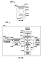
- FIGS 13A and 13B are system block diagrams illustrating an embodiment of a display device 2040.
- the display device 2040 can be, for example, a cellular or mobile telephone.
- the same components of display device 2040 or slight variations thereof are also illustrative of various types of display devices such as televisions and portable media players.
- the display device 2040 includes a housing 2041, a display 2030, an antenna 2043, a speaker 2045, an input device 2048, and a microphone 2046.
- the housing 2041 is generally formed from any of a variety of manufacturing processes as are well known to those of skill in the art, including injection molding, and vacuum forming.
- the housing 2041 may be made from any of a variety of materials, including but not limited to plastic, metal, glass, rubber, and ceramic, or a combination thereof.
- the housing 2041 includes removable portions (not shown) that may be interchanged with other removable portions of different color, or containing different logos, pictures, or symbols.
- the display 2030 of exemplary display device 2040 may be any of a variety of displays, including a bi-stable display, as described herein.
- the display 2030 includes a flat-panel display, such as plasma, EL, OLED, STN LCD, or TFT LCD as described above, or a non-flat-panel display, such as a CRT or other tube device, as is well known to those of skill in the art.
- the display 2030 includes an interferometric modulator display, as described herein.
- the components of one embodiment of exemplary display device 2040 are schematically illustrated in Figure 13B.
- the illustrated exemplary display device 2040 includes a housing 2041 and can include additional components at least partially enclosed therein.
- the exemplary display device 2040 includes a network interface 2027 that includes an antenna 2043 which is coupled to a transceiver 2047.
- the transceiver 2047 is connected to the processor 2021, which is connected to conditioning hardware 2052.
- the conditioning hardware 2052 may be configured to condition a signal (e.g. filter a signal).
- the conditioning hardware 2052 is connected to a speaker 2045 and a microphone 2046.
- the processor 2021 is also connected to an input device 2048 and a driver controller 2029.
- the driver controller 2029 is coupled to a frame buffer 2028 and to the array driver 2022, which in turn is coupled to a display array 2030.
- a power supply 2050 provides power to all components as required by the particular exemplary display device 2040 design.
- the network interface 2027 includes the antenna 2043 and the transceiver 2047 so that the exemplary display device 2040 can communicate with one or more devices over a network. In one embodiment the network interface 2027 may also have some processing capabilities to relieve requirements of the processor 2021.
- the antenna 2043 is any antenna known to those of skill in the art for transmitting and receiving signals. In one embodiment, the antenna transmits and receives RF signals according to the IEEE 802.11 standard, including IEEE 802.11(a), (b), or (g). In another embodiment, the antenna transmits and receives RF signals according to the BLUETOOTH standard. In the case of a cellular telephone, the antenna is designed to receive CDMA, GSM, AMPS or other known signals that are used to communicate within a wireless cell phone network.
- the transceiver 2047 pre-processes the signals received from the antenna 2043 so that they may be received by and further manipulated by the processor 2021.
- the transceiver 2047 also processes signals received from the processor 2021 so that they may be transmitted from the exemplary display device 2040 via the antenna 2043.
- the transceiver 2047 can be replaced by a receiver.
- network interface 2027 can be replaced by an image source, which can store or generate image data to be sent to the processor 2021.
- the image source can be a digital video disc (DVD) or a hard-disc drive that contains image data, or a software module that generates image data.
- Processor 2021 generally controls the overall operation of the exemplary display device 2040.
- the processor 2021 receives data, such as compressed image data from the network interface 2027 or an image source, and processes the data into raw image data or into a format that is readily processed into raw image data.
- the processor 2021 then sends the processed data to the driver controller 2029 or to frame buffer 2028 for storage.
- Raw data typically refers to the information that identifies the image characteristics at each location within an image. For example, such image characteristics can include color, saturation, and gray-scale level.
- the processor 2021 includes a microcontroller, CPU, or logic unit to control operation of the exemplary display device 2040.
- Conditioning hardware 2052 generally includes amplifiers and filters for transmitting signals to the speaker 2045, and for receiving signals from the microphone 2046.
- Conditioning hardware 2052 may be discrete components within the exemplary display device 2040, or may be incorporated within the processor 2021 or other components.
- the driver controller 2029 takes the raw image data generated by the processor 2021 either directly from the processor 2021 or from the frame buffer 2028 and reformats the raw image data appropriately for high speed transmission to the array driver 2022. Specifically, the driver controller 2029 reformats the raw image data into a data flow having a raster-like format, such that it has a time order suitable for scanning across the display array 2030. Then the driver controller 2029 sends the formatted information to the array driver 2022.
- a driver controller 2029 such as a LCD controller, is often associated with the system processor 2021 as a stand-alone Integrated Circuit (IC), such controllers may be implemented in many ways. They may be embedded in the processor 2021 as hardware, embedded in the processor 2021 as software, or fully integrated in hardware with the array driver 2022.
- IC Integrated Circuit
- the array driver 2022 receives the formatted information from the driver controller 2029 and reformats the video data into a parallel set of waveforms that are applied many times per second to the hundreds and sometimes thousands of leads coming from the display's x-y matrix of pixels.
- driver controller 2029, array driver 2022, and display array 2030 are appropriate for any of the types of displays described herein.
- driver controller 2029 is a conventional display controller or a bi-stable display controller (e.g., an interferometric modulator controller).
- array driver 2022 is a conventional driver or a bi-stable display driver (e.g., an interferometric modulator display).
- a driver controller 2029 is integrated with the array driver 2022.
- display array 2030 is a typical display array or a bi-stable display array (e.g., a display including an array of interferometric modulators).
- the input device 2048 allows a user to control the operation of the exemplary display device 2040.
- input device 2048 includes a keypad, such as a QWERTY keyboard or a telephone keypad, a button, a switch, a touch-sensitive screen, a pressure- or heat-sensitive membrane.
- the microphone 2046 is an input device for the exemplary display device 2040. When the microphone 2046 is used to input data to the device, voice commands may be provided by a user for controlling operations of the exemplary display device 2040.
- Power supply 2050 can include a variety of energy storage devices as are well known in the art.
- power supply 2050 is a rechargeable battery, such as a nickel-cadmium battery or a lithium ion battery.
- power supply 2050 is a renewable energy source, a capacitor, or a solar cell, including a plastic solar cell, and solar-cell paint.
- power supply 2050 is configured to receive power from a wall outlet.
- control programmability resides, as described above, in a driver controller which can be located in several places in the electronic display system. In some cases control programmability resides in the array driver 2022. Those of skill in the art will recognize that the above-described optimization may be implemented in any number of hardware and/or software components and in various configurations.
Landscapes
- Physics & Mathematics (AREA)
- General Physics & Mathematics (AREA)
- Engineering & Computer Science (AREA)
- Optics & Photonics (AREA)
- Nonlinear Science (AREA)
- Spectroscopy & Molecular Physics (AREA)
- Computer Hardware Design (AREA)
- Theoretical Computer Science (AREA)
- Mechanical Light Control Or Optical Switches (AREA)
- Devices For Indicating Variable Information By Combining Individual Elements (AREA)
- Micromachines (AREA)
Applications Claiming Priority (2)
| Application Number | Priority Date | Filing Date | Title |
|---|---|---|---|
| US61397704P | 2004-09-27 | 2004-09-27 | |
| US11/090,491 US7668415B2 (en) | 2004-09-27 | 2005-03-25 | Method and device for providing electronic circuitry on a backplate |
Publications (2)
| Publication Number | Publication Date |
|---|---|
| EP1655720A2 true EP1655720A2 (fr) | 2006-05-10 |
| EP1655720A3 EP1655720A3 (fr) | 2008-06-04 |
Family
ID=35958971
Family Applications (1)
| Application Number | Title | Priority Date | Filing Date |
|---|---|---|---|
| EP05255654A Withdrawn EP1655720A3 (fr) | 2004-09-27 | 2005-09-14 | Affichage électronique et méthode de fabrication de celui-ci |
Country Status (11)
| Country | Link |
|---|---|
| US (4) | US7668415B2 (fr) |
| EP (1) | EP1655720A3 (fr) |
| JP (3) | JP2006099101A (fr) |
| KR (1) | KR101237888B1 (fr) |
| AU (1) | AU2005204240A1 (fr) |
| BR (1) | BRPI0503855A (fr) |
| CA (1) | CA2518396A1 (fr) |
| MX (1) | MXPA05010090A (fr) |
| RU (1) | RU2005129919A (fr) |
| SG (2) | SG121140A1 (fr) |
| TW (1) | TW200626950A (fr) |
Families Citing this family (28)
| Publication number | Priority date | Publication date | Assignee | Title |
|---|---|---|---|---|
| JP4342174B2 (ja) * | 2002-12-27 | 2009-10-14 | 新光電気工業株式会社 | 電子デバイス及びその製造方法 |
| TWI251712B (en) * | 2003-08-15 | 2006-03-21 | Prime View Int Corp Ltd | Interference display plate |
| TW593127B (en) * | 2003-08-18 | 2004-06-21 | Prime View Int Co Ltd | Interference display plate and manufacturing method thereof |
| US7405924B2 (en) * | 2004-09-27 | 2008-07-29 | Idc, Llc | System and method for protecting microelectromechanical systems array using structurally reinforced back-plate |
| US7675669B2 (en) * | 2004-09-27 | 2010-03-09 | Qualcomm Mems Technologies, Inc. | Method and system for driving interferometric modulators |
| US7668415B2 (en) * | 2004-09-27 | 2010-02-23 | Qualcomm Mems Technologies, Inc. | Method and device for providing electronic circuitry on a backplate |
| US7999994B2 (en) | 2005-02-23 | 2011-08-16 | Pixtronix, Inc. | Display apparatus and methods for manufacture thereof |
| WO2007120885A2 (fr) * | 2006-04-13 | 2007-10-25 | Qualcomm Mems Technologies, Inc. | Dispositifs mems et procédé d'encapsulation desdits dispositifs |
| JP4903540B2 (ja) * | 2006-11-29 | 2012-03-28 | 京セラ株式会社 | 微小電子機械部品封止用基板及び複数個取り形態の微小電子機械部品封止用基板、並びに微小電子機械装置及び微小電子機械装置の製造方法 |
| JP2013061658A (ja) * | 2007-01-19 | 2013-04-04 | Pixtronix Inc | Memsディスプレイ装置 |
| US7719752B2 (en) * | 2007-05-11 | 2010-05-18 | Qualcomm Mems Technologies, Inc. | MEMS structures, methods of fabricating MEMS components on separate substrates and assembly of same |
| WO2009052326A2 (fr) * | 2007-10-19 | 2009-04-23 | Qualcomm Mems Technologies, Inc. | Dispositif d'affichage à éléments photovoltaïques intégrés |
| US20090323170A1 (en) * | 2008-06-30 | 2009-12-31 | Qualcomm Mems Technologies, Inc. | Groove on cover plate or substrate |
| WO2010044901A1 (fr) * | 2008-10-16 | 2010-04-22 | Qualcomm Mems Technologies, Inc. | Cellule photovoltaïque à couleur améliorée par modulateur interférométrique monolithique |
| US8379392B2 (en) * | 2009-10-23 | 2013-02-19 | Qualcomm Mems Technologies, Inc. | Light-based sealing and device packaging |
| US9090456B2 (en) * | 2009-11-16 | 2015-07-28 | Qualcomm Mems Technologies, Inc. | System and method of manufacturing an electromechanical device by printing raised conductive contours |
| WO2011130718A2 (fr) | 2010-04-16 | 2011-10-20 | Flex Lighting Ii, Llc | Dispositif d'éclairage frontal comprenant un guide de lumière basé sur un film |
| WO2011130715A2 (fr) | 2010-04-16 | 2011-10-20 | Flex Lighting Ii, Llc | Dispositif d'éclairage comprenant un guide de lumière basé sur un film |
| US8354747B1 (en) * | 2010-06-01 | 2013-01-15 | Amkor Technology, Inc | Conductive polymer lid for a sensor package and method therefor |
| KR101362398B1 (ko) | 2012-07-10 | 2014-02-13 | 앰코 테크놀로지 코리아 주식회사 | 반도체 패키지 및 그 제조 방법 |
| JP5746352B2 (ja) * | 2010-09-23 | 2015-07-08 | クゥアルコム・メムス・テクノロジーズ・インコーポレイテッドQUALCOMM MEMS Technologies, Inc. | 集積化された受動素子と電力増幅器 |
| US20120242638A1 (en) * | 2011-03-24 | 2012-09-27 | Qualcomm Mems Technologies, Inc. | Dielectric spacer for display devices |
| US8742570B2 (en) * | 2011-09-09 | 2014-06-03 | Qualcomm Mems Technologies, Inc. | Backplate interconnect with integrated passives |
| US8811636B2 (en) * | 2011-11-29 | 2014-08-19 | Qualcomm Mems Technologies, Inc. | Microspeaker with piezoelectric, metal and dielectric membrane |
| US10115671B2 (en) | 2012-08-03 | 2018-10-30 | Snaptrack, Inc. | Incorporation of passives and fine pitch through via for package on package |
| US20160232858A1 (en) * | 2015-02-11 | 2016-08-11 | Qualcomm Mems Technologies, Inc. | Creep resistant reflective structure in mems display |
| US10014189B2 (en) * | 2015-06-02 | 2018-07-03 | Ngk Spark Plug Co., Ltd. | Ceramic package with brazing material near seal member |
| KR20240011230A (ko) * | 2017-05-29 | 2024-01-25 | 본스인코오포레이티드 | 유리 밀봉 가스 방전 튜브 |
Citations (2)
| Publication number | Priority date | Publication date | Assignee | Title |
|---|---|---|---|---|
| US6589625B1 (en) | 2001-08-01 | 2003-07-08 | Iridigm Display Corporation | Hermetic seal and method to create the same |
| US20040051929A1 (en) | 1994-05-05 | 2004-03-18 | Sampsell Jeffrey Brian | Separable modulator |
Family Cites Families (362)
| Publication number | Priority date | Publication date | Assignee | Title |
|---|---|---|---|---|
| US444505A (en) * | 1891-01-13 | Temple for | ||
| US2534846A (en) | 1946-06-20 | 1950-12-19 | Emi Ltd | Color filter |
| DE1288651B (de) * | 1963-06-28 | 1969-02-06 | Siemens Ag | Anordnung elektrischer Dipole fuer Wellenlaengen unterhalb 1 mm und Verfahren zur Herstellung einer derartigen Anordnung |
| FR1603131A (fr) * | 1968-07-05 | 1971-03-22 | ||
| US3591839A (en) * | 1969-08-27 | 1971-07-06 | Siliconix Inc | Micro-electronic circuit with novel hermetic sealing structure and method of manufacture |
| US3813265A (en) | 1970-02-16 | 1974-05-28 | A Marks | Electro-optical dipolar material |
| US3653741A (en) * | 1970-02-16 | 1972-04-04 | Alvin M Marks | Electro-optical dipolar material |
| DE2336930A1 (de) | 1973-07-20 | 1975-02-06 | Battelle Institut E V | Infrarot-modulator (ii.) |
| US4036360A (en) | 1975-11-12 | 1977-07-19 | Graham Magnetics Incorporated | Package having dessicant composition |
| US4074480A (en) * | 1976-02-12 | 1978-02-21 | Burton Henry W G | Kit for converting single-glazed window to double-glazed window |
| US4099854A (en) | 1976-10-12 | 1978-07-11 | The Unites States Of America As Represented By The Secretary Of The Navy | Optical notch filter utilizing electric dipole resonance absorption |
| DE2802728C2 (de) | 1977-01-24 | 1984-03-15 | Sharp K.K., Osaka | Elektrochrome Anzeigezelle |
| US4389096A (en) | 1977-12-27 | 1983-06-21 | Matsushita Electric Industrial Co., Ltd. | Image display apparatus of liquid crystal valve projection type |
| US4663083A (en) | 1978-05-26 | 1987-05-05 | Marks Alvin M | Electro-optical dipole suspension with reflective-absorptive-transmissive characteristics |
| US4445050A (en) | 1981-12-15 | 1984-04-24 | Marks Alvin M | Device for conversion of light power to electric power |
| US4431691A (en) * | 1979-01-29 | 1984-02-14 | Tremco, Incorporated | Dimensionally stable sealant and spacer strip and composite structures comprising the same |
| US4228437A (en) | 1979-06-26 | 1980-10-14 | The United States Of America As Represented By The Secretary Of The Navy | Wideband polarization-transforming electromagnetic mirror |
| NL8001281A (nl) | 1980-03-04 | 1981-10-01 | Philips Nv | Weergeefinrichting. |
| CH633902A5 (fr) | 1980-03-11 | 1982-12-31 | Centre Electron Horloger | Dispositif de modulation de lumiere. |
| US4377324A (en) * | 1980-08-04 | 1983-03-22 | Honeywell Inc. | Graded index Fabry-Perot optical filter device |
| US4441791A (en) * | 1980-09-02 | 1984-04-10 | Texas Instruments Incorporated | Deformable mirror light modulator |
| FR2506026A1 (fr) | 1981-05-18 | 1982-11-19 | Radant Etudes | Procede et dispositif pour l'analyse d'un faisceau de rayonnement d'ondes electromagnetiques hyperfrequence |
| NL8103377A (nl) | 1981-07-16 | 1983-02-16 | Philips Nv | Weergeefinrichting. |
| US4571603A (en) * | 1981-11-03 | 1986-02-18 | Texas Instruments Incorporated | Deformable mirror electrostatic printer |
| NL8200354A (nl) | 1982-02-01 | 1983-09-01 | Philips Nv | Passieve weergeefinrichting. |
| US4500171A (en) * | 1982-06-02 | 1985-02-19 | Texas Instruments Incorporated | Process for plastic LCD fill hole sealing |
| US4482213A (en) | 1982-11-23 | 1984-11-13 | Texas Instruments Incorporated | Perimeter seal reinforcement holes for plastic LCDs |
| US4710732A (en) | 1984-07-31 | 1987-12-01 | Texas Instruments Incorporated | Spatial light modulator and method |
| US4566935A (en) * | 1984-07-31 | 1986-01-28 | Texas Instruments Incorporated | Spatial light modulator and method |
| US4662746A (en) | 1985-10-30 | 1987-05-05 | Texas Instruments Incorporated | Spatial light modulator and method |
| US5061049A (en) | 1984-08-31 | 1991-10-29 | Texas Instruments Incorporated | Spatial light modulator and method |
| US5096279A (en) * | 1984-08-31 | 1992-03-17 | Texas Instruments Incorporated | Spatial light modulator and method |
| US4596992A (en) | 1984-08-31 | 1986-06-24 | Texas Instruments Incorporated | Linear spatial light modulator and printer |
| US4615595A (en) | 1984-10-10 | 1986-10-07 | Texas Instruments Incorporated | Frame addressed spatial light modulator |
| US5172262A (en) | 1985-10-30 | 1992-12-15 | Texas Instruments Incorporated | Spatial light modulator and method |
| US5835255A (en) | 1986-04-23 | 1998-11-10 | Etalon, Inc. | Visible spectrum modulator arrays |
| GB8610129D0 (en) | 1986-04-25 | 1986-05-29 | Secr Defence | Electro-optical device |
| US4748366A (en) | 1986-09-02 | 1988-05-31 | Taylor George W | Novel uses of piezoelectric materials for creating optical effects |
| US4786128A (en) | 1986-12-02 | 1988-11-22 | Quantum Diagnostics, Ltd. | Device for modulating and reflecting electromagnetic radiation employing electro-optic layer having a variable index of refraction |
| US4977009A (en) | 1987-12-16 | 1990-12-11 | Ford Motor Company | Composite polymer/desiccant coatings for IC encapsulation |
| US4956619A (en) | 1988-02-19 | 1990-09-11 | Texas Instruments Incorporated | Spatial light modulator |
| US4856863A (en) | 1988-06-22 | 1989-08-15 | Texas Instruments Incorporated | Optical fiber interconnection network including spatial light modulator |
| US5028939A (en) | 1988-08-23 | 1991-07-02 | Texas Instruments Incorporated | Spatial light modulator system |
| US4982184A (en) * | 1989-01-03 | 1991-01-01 | General Electric Company | Electrocrystallochromic display and element |
| US5214419A (en) | 1989-02-27 | 1993-05-25 | Texas Instruments Incorporated | Planarized true three dimensional display |
| US5170156A (en) | 1989-02-27 | 1992-12-08 | Texas Instruments Incorporated | Multi-frequency two dimensional display system |
| US5446479A (en) | 1989-02-27 | 1995-08-29 | Texas Instruments Incorporated | Multi-dimensional array video processor system |
| KR100202246B1 (ko) * | 1989-02-27 | 1999-06-15 | 윌리엄 비. 켐플러 | 디지탈화 비디오 시스템을 위한 장치 및 방법 |
| US5162787A (en) | 1989-02-27 | 1992-11-10 | Texas Instruments Incorporated | Apparatus and method for digitized video system utilizing a moving display surface |
| US5272473A (en) | 1989-02-27 | 1993-12-21 | Texas Instruments Incorporated | Reduced-speckle display system |
| US5079544A (en) * | 1989-02-27 | 1992-01-07 | Texas Instruments Incorporated | Standard independent digitized video system |
| US5206629A (en) * | 1989-02-27 | 1993-04-27 | Texas Instruments Incorporated | Spatial light modulator and memory for digitized video display |
| US5287096A (en) * | 1989-02-27 | 1994-02-15 | Texas Instruments Incorporated | Variable luminosity display system |
| US5192946A (en) * | 1989-02-27 | 1993-03-09 | Texas Instruments Incorporated | Digitized color video display system |
| US5214420A (en) | 1989-02-27 | 1993-05-25 | Texas Instruments Incorporated | Spatial light modulator projection system with random polarity light |
| US5022745A (en) | 1989-09-07 | 1991-06-11 | Massachusetts Institute Of Technology | Electrostatically deformable single crystal dielectrically coated mirror |
| US4954789A (en) | 1989-09-28 | 1990-09-04 | Texas Instruments Incorporated | Spatial light modulator |
| US5381253A (en) * | 1991-11-14 | 1995-01-10 | Board Of Regents Of University Of Colorado | Chiral smectic liquid crystal optical modulators having variable retardation |
| US5124834A (en) | 1989-11-16 | 1992-06-23 | General Electric Company | Transferrable, self-supporting pellicle for elastomer light valve displays and method for making the same |
| US5037173A (en) | 1989-11-22 | 1991-08-06 | Texas Instruments Incorporated | Optical interconnection network |
| US5500635A (en) * | 1990-02-20 | 1996-03-19 | Mott; Jonathan C. | Products incorporating piezoelectric material |
| CH682523A5 (fr) * | 1990-04-20 | 1993-09-30 | Suisse Electronique Microtech | Dispositif de modulation de lumière à adressage matriciel. |
| GB9012099D0 (en) | 1990-05-31 | 1990-07-18 | Kodak Ltd | Optical article for multicolour imaging |
| US5099353A (en) * | 1990-06-29 | 1992-03-24 | Texas Instruments Incorporated | Architecture and process for integrating DMD with control circuit substrates |
| US5142405A (en) | 1990-06-29 | 1992-08-25 | Texas Instruments Incorporated | Bistable dmd addressing circuit and method |
| DE69113150T2 (de) | 1990-06-29 | 1996-04-04 | Texas Instruments Inc | Deformierbare Spiegelvorrichtung mit aktualisiertem Raster. |
| US5216537A (en) | 1990-06-29 | 1993-06-01 | Texas Instruments Incorporated | Architecture and process for integrating DMD with control circuit substrates |
| US5018256A (en) | 1990-06-29 | 1991-05-28 | Texas Instruments Incorporated | Architecture and process for integrating DMD with control circuit substrates |
| US5083857A (en) * | 1990-06-29 | 1992-01-28 | Texas Instruments Incorporated | Multi-level deformable mirror device |
| US5304419A (en) * | 1990-07-06 | 1994-04-19 | Alpha Fry Ltd | Moisture and particle getter for enclosures |
| US5153771A (en) | 1990-07-18 | 1992-10-06 | Northrop Corporation | Coherent light modulation and detector |
| US5192395A (en) * | 1990-10-12 | 1993-03-09 | Texas Instruments Incorporated | Method of making a digital flexure beam accelerometer |
| US5526688A (en) | 1990-10-12 | 1996-06-18 | Texas Instruments Incorporated | Digital flexure beam accelerometer and method |
| US5044736A (en) | 1990-11-06 | 1991-09-03 | Motorola, Inc. | Configurable optical filter or display |
| US5602671A (en) * | 1990-11-13 | 1997-02-11 | Texas Instruments Incorporated | Low surface energy passivation layer for micromechanical devices |
| US5331454A (en) | 1990-11-13 | 1994-07-19 | Texas Instruments Incorporated | Low reset voltage process for DMD |
| US5233459A (en) | 1991-03-06 | 1993-08-03 | Massachusetts Institute Of Technology | Electric display device |
| CA2063744C (fr) | 1991-04-01 | 2002-10-08 | Paul M. Urbanus | Architecture et dispositif de synchronisation de systeme d'affichage a modulation d'impulsions en duree |
| US5142414A (en) | 1991-04-22 | 1992-08-25 | Koehler Dale R | Electrically actuatable temporal tristimulus-color device |
| US5226099A (en) | 1991-04-26 | 1993-07-06 | Texas Instruments Incorporated | Digital micromirror shutter device |
| US5268533A (en) | 1991-05-03 | 1993-12-07 | Hughes Aircraft Company | Pre-stressed laminated lid for electronic circuit package |
| US5179274A (en) * | 1991-07-12 | 1993-01-12 | Texas Instruments Incorporated | Method for controlling operation of optical systems and devices |
| US5168406A (en) | 1991-07-31 | 1992-12-01 | Texas Instruments Incorporated | Color deformable mirror device and method for manufacture |
| US5254980A (en) | 1991-09-06 | 1993-10-19 | Texas Instruments Incorporated | DMD display system controller |
| US5563398A (en) | 1991-10-31 | 1996-10-08 | Texas Instruments Incorporated | Spatial light modulator scanning system |
| CA2081753C (fr) | 1991-11-22 | 2002-08-06 | Jeffrey B. Sampsell | Dispositif de balayage a miroir deformable |
| DE59206487D1 (de) * | 1991-11-26 | 1996-07-11 | Siemens Ag | Phenylchinoxalin-Copolymere |
| US5233385A (en) | 1991-12-18 | 1993-08-03 | Texas Instruments Incorporated | White light enhanced color field sequential projection |
| US5233456A (en) | 1991-12-20 | 1993-08-03 | Texas Instruments Incorporated | Resonant mirror and method of manufacture |
| US5244707A (en) | 1992-01-10 | 1993-09-14 | Shores A Andrew | Enclosure for electronic devices |
| CA2087625C (fr) | 1992-01-23 | 2006-12-12 | William E. Nelson | Retard non systolique et impression integree |
| US5296950A (en) * | 1992-01-31 | 1994-03-22 | Texas Instruments Incorporated | Optical signal free-space conversion board |
| US5231532A (en) | 1992-02-05 | 1993-07-27 | Texas Instruments Incorporated | Switchable resonant filter for optical radiation |
| DE69310974T2 (de) | 1992-03-25 | 1997-11-06 | Texas Instruments Inc | Eingebautes optisches Eichsystem |
| US5312513A (en) | 1992-04-03 | 1994-05-17 | Texas Instruments Incorporated | Methods of forming multiple phase light modulators |
| WO1993021663A1 (fr) * | 1992-04-08 | 1993-10-28 | Georgia Tech Research Corporation | Procede d'arrachement de materiaux en couche mince d'un substrat de croissance |
| US5311360A (en) | 1992-04-28 | 1994-05-10 | The Board Of Trustees Of The Leland Stanford, Junior University | Method and apparatus for modulating a light beam |
| DE69309780T2 (de) * | 1992-05-19 | 1997-10-23 | Canon Kk | Verfahren und Einrichtung zur Steuerung einer Anzeige |
| JPH0651250A (ja) * | 1992-05-20 | 1994-02-25 | Texas Instr Inc <Ti> | モノリシックな空間的光変調器およびメモリのパッケージ |
| JPH06214169A (ja) * | 1992-06-08 | 1994-08-05 | Texas Instr Inc <Ti> | 制御可能な光学的周期的表面フィルタ |
| US5818095A (en) * | 1992-08-11 | 1998-10-06 | Texas Instruments Incorporated | High-yield spatial light modulator with light blocking layer |
| US5327286A (en) | 1992-08-31 | 1994-07-05 | Texas Instruments Incorporated | Real time optical correlation system |
| US5325116A (en) | 1992-09-18 | 1994-06-28 | Texas Instruments Incorporated | Device for writing to and reading from optical storage media |
| US5659374A (en) | 1992-10-23 | 1997-08-19 | Texas Instruments Incorporated | Method of repairing defective pixels |
| US5322161A (en) | 1992-11-30 | 1994-06-21 | United States Surgical Corporation | Clear package for bioabsorbable articles |
| CN1057614C (zh) | 1993-01-11 | 2000-10-18 | 德克萨斯仪器股份有限公司 | 用于空间光调制器的象素控制电路 |
| US6674562B1 (en) * | 1994-05-05 | 2004-01-06 | Iridigm Display Corporation | Interferometric modulation of radiation |
| US5461411A (en) | 1993-03-29 | 1995-10-24 | Texas Instruments Incorporated | Process and architecture for digital micromirror printer |
| DE4317274A1 (de) * | 1993-05-25 | 1994-12-01 | Bosch Gmbh Robert | Verfahren zur Herstellung oberflächen-mikromechanischer Strukturen |
| US5489952A (en) * | 1993-07-14 | 1996-02-06 | Texas Instruments Incorporated | Method and device for multi-format television |
| US5365283A (en) | 1993-07-19 | 1994-11-15 | Texas Instruments Incorporated | Color phase control for projection display using spatial light modulator |
| US5526172A (en) | 1993-07-27 | 1996-06-11 | Texas Instruments Incorporated | Microminiature, monolithic, variable electrical signal processor and apparatus including same |
| US5581272A (en) | 1993-08-25 | 1996-12-03 | Texas Instruments Incorporated | Signal generator for controlling a spatial light modulator |
| FR2710161B1 (fr) | 1993-09-13 | 1995-11-24 | Suisse Electronique Microtech | Réseau miniature d'obturateurs de lumière. |
| US5457493A (en) | 1993-09-15 | 1995-10-10 | Texas Instruments Incorporated | Digital micro-mirror based image simulation system |
| US5526051A (en) | 1993-10-27 | 1996-06-11 | Texas Instruments Incorporated | Digital television system |
| US5497197A (en) * | 1993-11-04 | 1996-03-05 | Texas Instruments Incorporated | System and method for packaging data into video processor |
| US5459602A (en) | 1993-10-29 | 1995-10-17 | Texas Instruments | Micro-mechanical optical shutter |
| US5452024A (en) | 1993-11-01 | 1995-09-19 | Texas Instruments Incorporated | DMD display system |
| US5385255A (en) * | 1993-11-23 | 1995-01-31 | Sherwood Tool, Inc. | Snap-on lid |
| US5517347A (en) | 1993-12-01 | 1996-05-14 | Texas Instruments Incorporated | Direct view deformable mirror device |
| CA2137059C (fr) | 1993-12-03 | 2004-11-23 | Texas Instruments Incorporated | Architecture servant a accroitre la definition horizontale dans les terminaux de transmission de messages |
| US5583688A (en) | 1993-12-21 | 1996-12-10 | Texas Instruments Incorporated | Multi-level digital micromirror device |
| US5448314A (en) | 1994-01-07 | 1995-09-05 | Texas Instruments | Method and apparatus for sequential color imaging |
| US5500761A (en) * | 1994-01-27 | 1996-03-19 | At&T Corp. | Micromechanical modulator |
| US5444566A (en) | 1994-03-07 | 1995-08-22 | Texas Instruments Incorporated | Optimized electronic operation of digital micromirror devices |
| US5665997A (en) | 1994-03-31 | 1997-09-09 | Texas Instruments Incorporated | Grated landing area to eliminate sticking of micro-mechanical devices |
| US7550794B2 (en) * | 2002-09-20 | 2009-06-23 | Idc, Llc | Micromechanical systems device comprising a displaceable electrode and a charge-trapping layer |
| US6040937A (en) * | 1994-05-05 | 2000-03-21 | Etalon, Inc. | Interferometric modulation |
| US20010003487A1 (en) | 1996-11-05 | 2001-06-14 | Mark W. Miles | Visible spectrum modulator arrays |
| US7123216B1 (en) | 1994-05-05 | 2006-10-17 | Idc, Llc | Photonic MEMS and structures |
| US6710908B2 (en) * | 1994-05-05 | 2004-03-23 | Iridigm Display Corporation | Controlling micro-electro-mechanical cavities |
| US6680792B2 (en) | 1994-05-05 | 2004-01-20 | Iridigm Display Corporation | Interferometric modulation of radiation |
| US5451552A (en) * | 1994-05-13 | 1995-09-19 | Hughes Aircraft Company | Method for improvement of optical quality and reduction of background doping in gainSB/INAS superlattices |
| EP0686934B1 (fr) | 1994-05-17 | 2001-09-26 | Texas Instruments Incorporated | Dispositif de visualisation avec détection de la position d'une aiguille |
| US5497172A (en) * | 1994-06-13 | 1996-03-05 | Texas Instruments Incorporated | Pulse width modulation for spatial light modulator with split reset addressing |
| US5673106A (en) | 1994-06-17 | 1997-09-30 | Texas Instruments Incorporated | Printing system with self-monitoring and adjustment |
| US5454906A (en) | 1994-06-21 | 1995-10-03 | Texas Instruments Inc. | Method of providing sacrificial spacer for micro-mechanical devices |
| US5499062A (en) * | 1994-06-23 | 1996-03-12 | Texas Instruments Incorporated | Multiplexed memory timing with block reset and secondary memory |
| US5485304A (en) | 1994-07-29 | 1996-01-16 | Texas Instruments, Inc. | Support posts for micro-mechanical devices |
| US5636052A (en) | 1994-07-29 | 1997-06-03 | Lucent Technologies Inc. | Direct view display based on a micromechanical modulation |
| US5703710A (en) | 1994-09-09 | 1997-12-30 | Deacon Research | Method for manipulating optical energy using poled structure |
| US6053617A (en) | 1994-09-23 | 2000-04-25 | Texas Instruments Incorporated | Manufacture method for micromechanical devices |
| US5619059A (en) * | 1994-09-28 | 1997-04-08 | National Research Council Of Canada | Color deformable mirror device having optical thin film interference color coatings |
| US5650881A (en) | 1994-11-02 | 1997-07-22 | Texas Instruments Incorporated | Support post architecture for micromechanical devices |
| US5552924A (en) | 1994-11-14 | 1996-09-03 | Texas Instruments Incorporated | Micromechanical device having an improved beam |
| US5610624A (en) * | 1994-11-30 | 1997-03-11 | Texas Instruments Incorporated | Spatial light modulator with reduced possibility of an on state defect |
| TW378276B (en) | 1995-01-13 | 2000-01-01 | Seiko Epson Corp | Liquid crystal display device and its fabrication method |
| JPH08263208A (ja) * | 1995-02-24 | 1996-10-11 | Whitaker Corp:The | 弾性波タッチパネル及びその製造方法 |
| US5567334A (en) | 1995-02-27 | 1996-10-22 | Texas Instruments Incorporated | Method for creating a digital micromirror device using an aluminum hard mask |
| US5610438A (en) * | 1995-03-08 | 1997-03-11 | Texas Instruments Incorporated | Micro-mechanical device with non-evaporable getter |
| US5535047A (en) | 1995-04-18 | 1996-07-09 | Texas Instruments Incorporated | Active yoke hidden hinge digital micromirror device |
| US5784190A (en) | 1995-04-27 | 1998-07-21 | John M. Baker | Electro-micro-mechanical shutters on transparent substrates |
| US6046840A (en) | 1995-06-19 | 2000-04-04 | Reflectivity, Inc. | Double substrate reflective spatial light modulator with self-limiting micro-mechanical elements |
| US6969635B2 (en) * | 2000-12-07 | 2005-11-29 | Reflectivity, Inc. | Methods for depositing, releasing and packaging micro-electromechanical devices on wafer substrates |
| US5837562A (en) | 1995-07-07 | 1998-11-17 | The Charles Stark Draper Laboratory, Inc. | Process for bonding a shell to a substrate for packaging a semiconductor |
| US5739945A (en) * | 1995-09-29 | 1998-04-14 | Tayebati; Parviz | Electrically tunable optical filter utilizing a deformable multi-layer mirror |
| US7907319B2 (en) | 1995-11-06 | 2011-03-15 | Qualcomm Mems Technologies, Inc. | Method and device for modulating light with optical compensation |
| US5999306A (en) | 1995-12-01 | 1999-12-07 | Seiko Epson Corporation | Method of manufacturing spatial light modulator and electronic device employing it |
| US5825528A (en) | 1995-12-26 | 1998-10-20 | Lucent Technologies Inc. | Phase-mismatched fabry-perot cavity micromechanical modulator |
| JP3799092B2 (ja) * | 1995-12-29 | 2006-07-19 | アジレント・テクノロジーズ・インク | 光変調装置及びディスプレイ装置 |
| US5771321A (en) | 1996-01-04 | 1998-06-23 | Massachusetts Institute Of Technology | Micromechanical optical switch and flat panel display |
| US5784166A (en) | 1996-04-03 | 1998-07-21 | Nikon Corporation | Position resolution of an interferometrially controlled moving stage by regression analysis |
| US5815141A (en) | 1996-04-12 | 1998-09-29 | Elo Touch Systems, Inc. | Resistive touchscreen having multiple selectable regions for pressure discrimination |
| US5939785A (en) | 1996-04-12 | 1999-08-17 | Texas Instruments Incorporated | Micromechanical device including time-release passivant |
| US5936758A (en) | 1996-04-12 | 1999-08-10 | Texas Instruments Incorporated | Method of passivating a micromechanical device within a hermetic package |
| US5853662A (en) | 1996-04-17 | 1998-12-29 | Mitsubishi Gas Chemical Company, Inc. | Method for preserving polished inorganic glass and method for preserving article obtained by using the same |
| US5710656A (en) * | 1996-07-30 | 1998-01-20 | Lucent Technologies Inc. | Micromechanical optical modulator having a reduced-mass composite membrane |
| US5789848A (en) | 1996-08-02 | 1998-08-04 | Motorola, Inc. | Field emission display having a cathode reinforcement member |
| US6025767A (en) * | 1996-08-05 | 2000-02-15 | Mcnc | Encapsulated micro-relay modules and methods of fabricating same |
| US5912758A (en) | 1996-09-11 | 1999-06-15 | Texas Instruments Incorporated | Bipolar reset for spatial light modulators |
| US5771116A (en) | 1996-10-21 | 1998-06-23 | Texas Instruments Incorporated | Multiple bias level reset waveform for enhanced DMD control |
| JP3695494B2 (ja) | 1996-11-13 | 2005-09-14 | セイコーエプソン株式会社 | 光変調デバイス、その製造方法および表示装置 |
| JP3208658B2 (ja) | 1997-03-27 | 2001-09-17 | 株式会社アドバンスト・ディスプレイ | 電気光学素子の製法 |
| EP0877272B1 (fr) * | 1997-05-08 | 2002-07-31 | Texas Instruments Incorporated | Améliorations concernant les modulateurs de lumière spatiaux |
| US6480177B2 (en) | 1997-06-04 | 2002-11-12 | Texas Instruments Incorporated | Blocked stepped address voltage for micromechanical devices |
| GB9724077D0 (en) | 1997-11-15 | 1998-01-14 | Dow Corning Sa | Insulating glass units |
| US6028690A (en) * | 1997-11-26 | 2000-02-22 | Texas Instruments Incorporated | Reduced micromirror mirror gaps for improved contrast ratio |
| US6180428B1 (en) * | 1997-12-12 | 2001-01-30 | Xerox Corporation | Monolithic scanning light emitting devices using micromachining |
| JP2876530B1 (ja) | 1998-02-24 | 1999-03-31 | 東京工業大学長 | 固着した可動部の修復手段を具える超小型素子およびその製造方法 |
| US6195196B1 (en) * | 1998-03-13 | 2001-02-27 | Fuji Photo Film Co., Ltd. | Array-type exposing device and flat type display incorporating light modulator and driving method thereof |
| WO1999052006A2 (fr) | 1998-04-08 | 1999-10-14 | Etalon, Inc. | Modulation interferometrique de rayonnement |
| DE69808318T2 (de) * | 1998-04-17 | 2003-01-23 | Seiko Epson Corp | Herstellungsverfahren einer lichtmodulationsvorrichtung und projektor |
| US6160833A (en) | 1998-05-06 | 2000-12-12 | Xerox Corporation | Blue vertical cavity surface emitting laser |
| US6282010B1 (en) | 1998-05-14 | 2001-08-28 | Texas Instruments Incorporated | Anti-reflective coatings for spatial light modulators |
| US6323982B1 (en) | 1998-05-22 | 2001-11-27 | Texas Instruments Incorporated | Yield superstructure for digital micromirror device |
| JPH11337953A (ja) * | 1998-05-25 | 1999-12-10 | Toshiba Corp | 液晶表示装置 |
| US6147790A (en) | 1998-06-02 | 2000-11-14 | Texas Instruments Incorporated | Spring-ring micromechanical device |
| US6295154B1 (en) | 1998-06-05 | 2001-09-25 | Texas Instruments Incorporated | Optical switching apparatus |
| JP2000003783A (ja) | 1998-06-12 | 2000-01-07 | Tdk Corp | 有機el表示装置 |
| US6496122B2 (en) | 1998-06-26 | 2002-12-17 | Sharp Laboratories Of America, Inc. | Image display and remote control system capable of displaying two distinct images |
| US6303986B1 (en) | 1998-07-29 | 2001-10-16 | Silicon Light Machines | Method of and apparatus for sealing an hermetic lid to a semiconductor die |
| US6113239A (en) | 1998-09-04 | 2000-09-05 | Sharp Laboratories Of America, Inc. | Projection display system for reflective light valves |
| US6365229B1 (en) | 1998-09-30 | 2002-04-02 | Texas Instruments Incorporated | Surface treatment material deposition and recapture |
| US6843936B1 (en) | 1998-10-22 | 2005-01-18 | Texas Instruments Incorporated | Getter for enhanced micromechanical device performance |
| US6004179A (en) | 1998-10-26 | 1999-12-21 | Micron Technology, Inc. | Methods of fabricating flat panel evacuated displays |
| GB9827965D0 (en) * | 1998-12-19 | 1999-02-10 | Secr Defence | Assembly of cells having spaced opposed substrates |
| GB9827900D0 (en) * | 1998-12-19 | 1999-02-10 | Secr Defence | Spacers for cells having spaced opposed substrates |
| US6245194B1 (en) | 1998-12-21 | 2001-06-12 | Sikorsky Aircraft Corporation | Processed fiber for emission of energy into a medium and method therefor |
| US6606175B1 (en) | 1999-03-16 | 2003-08-12 | Sharp Laboratories Of America, Inc. | Multi-segment light-emitting diode |
| KR20000071852A (ko) * | 1999-04-30 | 2000-11-25 | 모리시타 요이찌 | 액정표시소자 및 그 제조방법 |
| US6201633B1 (en) * | 1999-06-07 | 2001-03-13 | Xerox Corporation | Micro-electromechanical based bistable color display sheets |
| US6862029B1 (en) * | 1999-07-27 | 2005-03-01 | Hewlett-Packard Development Company, L.P. | Color display system |
| US6833668B1 (en) | 1999-09-29 | 2004-12-21 | Sanyo Electric Co., Ltd. | Electroluminescence display device having a desiccant |
| WO2003007049A1 (fr) | 1999-10-05 | 2003-01-23 | Iridigm Display Corporation | Mems et structures photoniques |
| US6400009B1 (en) * | 1999-10-15 | 2002-06-04 | Lucent Technologies Inc. | Hermatic firewall for MEMS packaging in flip-chip bonded geometry |
| US6549338B1 (en) | 1999-11-12 | 2003-04-15 | Texas Instruments Incorporated | Bandpass filter to reduce thermal impact of dichroic light shift |
| US6472739B1 (en) | 1999-11-15 | 2002-10-29 | Jds Uniphase Corporation | Encapsulated microelectromechanical (MEMS) devices |
| US6552840B2 (en) | 1999-12-03 | 2003-04-22 | Texas Instruments Incorporated | Electrostatic efficiency of micromechanical devices |
| DE69933380T2 (de) | 1999-12-15 | 2007-08-02 | Asulab S.A. | Verfahren zum hermetischen Einkapseln von Mikrosystemen vor Ort |
| US6548908B2 (en) | 1999-12-27 | 2003-04-15 | Xerox Corporation | Structure and method for planar lateral oxidation in passive devices |
| US6545335B1 (en) | 1999-12-27 | 2003-04-08 | Xerox Corporation | Structure and method for electrical isolation of optoelectronic integrated circuits |
| US6583921B2 (en) | 1999-12-28 | 2003-06-24 | Texas Instruments Incorporated | Micromechanical device and method for non-contacting edge-coupled operation |
| JP2001249287A (ja) | 1999-12-30 | 2001-09-14 | Texas Instr Inc <Ti> | 双安定マイクロミラー・アレイを動作させる方法 |
| DE10004964B4 (de) | 2000-02-04 | 2010-07-29 | Robert Bosch Gmbh | Mikromechanische Kappenstruktur |
| GB2359216B (en) | 2000-02-11 | 2003-10-29 | Purple Voice Ltd | A method of synchronising the replay of audio data in a network of computers |
| JP2001318324A (ja) | 2000-05-11 | 2001-11-16 | Seiko Epson Corp | 光スイッチングユニット、その製造方法および画像表示装置 |
| US6661084B1 (en) | 2000-05-16 | 2003-12-09 | Sandia Corporation | Single level microelectronic device package with an integral window |
| US6379988B1 (en) | 2000-05-16 | 2002-04-30 | Sandia Corporation | Pre-release plastic packaging of MEMS and IMEMS devices |
| US6384473B1 (en) * | 2000-05-16 | 2002-05-07 | Sandia Corporation | Microelectronic device package with an integral window |
| JP2001351998A (ja) | 2000-06-09 | 2001-12-21 | Kyocera Corp | 半導体素子収納用パッケージ |
| US6686653B2 (en) | 2000-06-28 | 2004-02-03 | Institut National D'optique | Miniature microdevice package and process for making thereof |
| US6473274B1 (en) | 2000-06-28 | 2002-10-29 | Texas Instruments Incorporated | Symmetrical microactuator structure for use in mass data storage devices, or the like |
| KR100840827B1 (ko) | 2000-07-03 | 2008-06-23 | 소니 가부시끼 가이샤 | 광학 다층 구조체, 광학 절환 장치 및 화상 디스플레이 |
| US6853129B1 (en) * | 2000-07-28 | 2005-02-08 | Candescent Technologies Corporation | Protected substrate structure for a field emission display device |
| US6778155B2 (en) | 2000-07-31 | 2004-08-17 | Texas Instruments Incorporated | Display operation with inserted block clears |
| TWI251101B (en) | 2000-08-02 | 2006-03-11 | Allied Material Technology Cor | A liquid crystal display and a method for fabricating the same |
| JP2002062492A (ja) | 2000-08-15 | 2002-02-28 | Canon Inc | 干渉性変調素子を用いた投影光学系 |
| JP2002062491A (ja) | 2000-08-15 | 2002-02-28 | Canon Inc | 干渉性変調素子を用いた撮像光学系及び光量制御装置 |
| US6643069B2 (en) | 2000-08-31 | 2003-11-04 | Texas Instruments Incorporated | SLM-base color projection display having multiple SLM's and multiple projection lenses |
| US6466354B1 (en) * | 2000-09-19 | 2002-10-15 | Silicon Light Machines | Method and apparatus for interferometric modulation of light |
| US6426461B1 (en) | 2000-09-21 | 2002-07-30 | Delphi Technologies, Inc. | Enclosure for electronic components |
| DE10049288B4 (de) * | 2000-10-04 | 2004-07-15 | Infineon Technologies Ag | Elektronische Bauteile und eine Folienband zum Verpacken von Bonddrahtverbindungen elektronischer Bauteile sowie deren Herstellungsverfahren |
| SK4612003A3 (en) | 2000-10-20 | 2004-06-08 | Pfizer Prod Inc | Alpha-aryl ethanolamines and their use as beta-3 adrenergic receptor agonists |
| US6859218B1 (en) * | 2000-11-07 | 2005-02-22 | Hewlett-Packard Development Company, L.P. | Electronic display devices and methods |
| US7178927B2 (en) | 2000-11-14 | 2007-02-20 | Semiconductor Energy Laboratory Co., Ltd. | Electroluminescent device having drying agent |
| US6762868B2 (en) | 2000-11-16 | 2004-07-13 | Texas Instruments Incorporated | Electro-optical package with drop-in aperture |
| US6664779B2 (en) | 2000-11-16 | 2003-12-16 | Texas Instruments Incorporated | Package with environmental control material carrier |
| AU2002237682A1 (en) | 2000-11-27 | 2002-06-03 | Microsensors Inc. | Wafer eutectic bonding of mems gyros |
| US20020075551A1 (en) | 2000-11-29 | 2002-06-20 | Onix Microsystems, Inc | Enclosure for MEMS apparatus and method of using the same |
| US7307775B2 (en) | 2000-12-07 | 2007-12-11 | Texas Instruments Incorporated | Methods for depositing, releasing and packaging micro-electromechanical devices on wafer substrates |
| US6906847B2 (en) | 2000-12-07 | 2005-06-14 | Reflectivity, Inc | Spatial light modulators with light blocking/absorbing areas |
| US6775174B2 (en) | 2000-12-28 | 2004-08-10 | Texas Instruments Incorporated | Memory architecture for micromirror cell |
| US6625047B2 (en) | 2000-12-31 | 2003-09-23 | Texas Instruments Incorporated | Micromechanical memory element |
| JP2002296519A (ja) | 2001-03-29 | 2002-10-09 | Ricoh Co Ltd | 光変調装置及びその光変調装置の製造方法並びにその光変調装置を具備する画像形成装置及びその光変調装置を具備する画像投影表示装置 |
| JP2002258310A (ja) | 2001-02-28 | 2002-09-11 | Kyocera Corp | 液晶表示装置および表示機器 |
| US6455927B1 (en) | 2001-03-12 | 2002-09-24 | Amkor Technology, Inc. | Micromirror device package |
| US6630786B2 (en) | 2001-03-30 | 2003-10-07 | Candescent Technologies Corporation | Light-emitting device having light-reflective layer formed with, or/and adjacent to, material that enhances device performance |
| US6531767B2 (en) * | 2001-04-09 | 2003-03-11 | Analog Devices Inc. | Critically aligned optical MEMS dies for large packaged substrate arrays and method of manufacture |
| JP2002311843A (ja) | 2001-04-17 | 2002-10-25 | Dainippon Printing Co Ltd | 電磁波遮蔽用部材及びディスプレイ |
| JP2002312066A (ja) | 2001-04-17 | 2002-10-25 | Hunet Inc | 着脱自在な増設ディスプレイを備えた携帯用コンピュータ及び増設用ディスプレイモジュール |
| KR100387239B1 (ko) | 2001-04-26 | 2003-06-12 | 삼성전자주식회사 | Mems 릴레이 및 그 제조방법 |
| US6465355B1 (en) | 2001-04-27 | 2002-10-15 | Hewlett-Packard Company | Method of fabricating suspended microstructures |
| JP2002328313A (ja) | 2001-05-01 | 2002-11-15 | Sony Corp | 光スイッチング素子およびその製造方法、並びに画像表示装置 |
| US6706316B2 (en) | 2001-05-08 | 2004-03-16 | Eastman Kodak Company | Ultrasonically sealing the cover plate to provide a hermetic enclosure for OLED displays |
| US6558820B2 (en) * | 2001-05-10 | 2003-05-06 | Eastman Kodak Company | High contrast light-emitting diode devices |
| US6822628B2 (en) | 2001-06-28 | 2004-11-23 | Candescent Intellectual Property Services, Inc. | Methods and systems for compensating row-to-row brightness variations of a field emission display |
| US6862022B2 (en) * | 2001-07-20 | 2005-03-01 | Hewlett-Packard Development Company, L.P. | Method and system for automatically selecting a vertical refresh rate for a video display monitor |
| US6922499B2 (en) | 2001-07-24 | 2005-07-26 | Lucent Technologies Inc. | MEMS driver circuit arrangement |
| US6600201B2 (en) | 2001-08-03 | 2003-07-29 | Hewlett-Packard Development Company, L.P. | Systems with high density packing of micromachines |
| US6632698B2 (en) | 2001-08-07 | 2003-10-14 | Hewlett-Packard Development Company, L.P. | Microelectromechanical device having a stiffened support beam, and methods of forming stiffened support beams in MEMS |
| US6778046B2 (en) | 2001-09-17 | 2004-08-17 | Magfusion Inc. | Latching micro magnetic relay packages and methods of packaging |
| US6590157B2 (en) | 2001-09-21 | 2003-07-08 | Eastman Kodak Company | Sealing structure for highly moisture-sensitive electronic device element and method for fabrication |
| US6893574B2 (en) | 2001-10-23 | 2005-05-17 | Analog Devices Inc | MEMS capping method and apparatus |
| US6870581B2 (en) * | 2001-10-30 | 2005-03-22 | Sharp Laboratories Of America, Inc. | Single panel color video projection display using reflective banded color falling-raster illumination |
| US6776538B2 (en) | 2001-12-12 | 2004-08-17 | Axsun Technologies, Inc. | MEMS tunable optical filter system with moisture getter for frequency stability |
| US7050835B2 (en) * | 2001-12-12 | 2006-05-23 | Universal Display Corporation | Intelligent multi-media display communication system |
| JP2003185496A (ja) | 2001-12-13 | 2003-07-03 | Mitsubishi Electric Corp | 赤外線検出アレイおよびその製造方法 |
| JP3755460B2 (ja) | 2001-12-26 | 2006-03-15 | ソニー株式会社 | 静電駆動型mems素子とその製造方法、光学mems素子、光変調素子、glvデバイス、レーザディスプレイ、及びmems装置 |
| JP4168757B2 (ja) | 2002-02-01 | 2008-10-22 | 松下電器産業株式会社 | フィルタ |
| JP2003228302A (ja) | 2002-02-04 | 2003-08-15 | Toshiba Electronic Engineering Corp | 表示装置及びその製造方法 |
| US6794119B2 (en) * | 2002-02-12 | 2004-09-21 | Iridigm Display Corporation | Method for fabricating a structure for a microelectromechanical systems (MEMS) device |
| JP4088864B2 (ja) | 2002-02-13 | 2008-05-21 | ソニー株式会社 | 光学多層構造体、これを用いた光スイッチング素子および画像表示装置 |
| US6574033B1 (en) | 2002-02-27 | 2003-06-03 | Iridigm Display Corporation | Microelectromechanical systems device and method for fabricating same |
| US7535093B1 (en) | 2002-03-08 | 2009-05-19 | Raytheon Company | Method and apparatus for packaging circuit devices |
| US6603182B1 (en) | 2002-03-12 | 2003-08-05 | Lucent Technologies Inc. | Packaging micromechanical devices |
| US7046374B1 (en) | 2002-03-14 | 2006-05-16 | Avanex Corporation | Interferometers for optical communications utilizing photo-sensitive materials |
| US6627814B1 (en) | 2002-03-22 | 2003-09-30 | David H. Stark | Hermetically sealed micro-device package with window |
| US6962834B2 (en) | 2002-03-22 | 2005-11-08 | Stark David H | Wafer-level hermetic micro-device packages |
| US7832177B2 (en) | 2002-03-22 | 2010-11-16 | Electronics Packaging Solutions, Inc. | Insulated glazing units |
| US6707351B2 (en) | 2002-03-27 | 2004-03-16 | Motorola, Inc. | Tunable MEMS resonator and method for tuning |
| US20030183916A1 (en) | 2002-03-27 | 2003-10-02 | John Heck | Packaging microelectromechanical systems |
| JP3558621B2 (ja) | 2002-04-15 | 2004-08-25 | シャープ株式会社 | 液晶表示装置 |
| US6954297B2 (en) | 2002-04-30 | 2005-10-11 | Hewlett-Packard Development Company, L.P. | Micro-mirror device including dielectrophoretic liquid |
| US20030202264A1 (en) | 2002-04-30 | 2003-10-30 | Weber Timothy L. | Micro-mirror device |
| US6972882B2 (en) | 2002-04-30 | 2005-12-06 | Hewlett-Packard Development Company, L.P. | Micro-mirror device with light angle amplification |
| US20040212026A1 (en) | 2002-05-07 | 2004-10-28 | Hewlett-Packard Company | MEMS device having time-varying control |
| JP3943437B2 (ja) | 2002-05-10 | 2007-07-11 | アルプス電気株式会社 | 液晶表示装置 |
| FR2839812B1 (fr) | 2002-05-17 | 2005-07-01 | Atmel Grenoble Sa | Procede de fabrication collective de composants de filtrage optique et plaquette de composants |
| TW589915B (en) * | 2002-05-24 | 2004-06-01 | Sanyo Electric Co | Electroluminescence display device |
| US7034984B2 (en) | 2002-06-19 | 2006-04-25 | Miradia Inc. | Fabrication of a high fill ratio reflective spatial light modulator with hidden hinge |
| FR2841380A1 (fr) | 2002-06-25 | 2003-12-26 | Commissariat Energie Atomique | Procede d'encapsulation d'un objet sous atmosphere controlee |
| ITTO20020551A1 (it) | 2002-06-26 | 2003-12-29 | Vhit Spa | Macchina fluidica a cilindrata variabile in funzione della pressione |
| US6741377B2 (en) | 2002-07-02 | 2004-05-25 | Iridigm Display Corporation | Device having a light-absorbing mask and a method for fabricating same |
| JP2004053852A (ja) | 2002-07-18 | 2004-02-19 | Sony Corp | 光変調素子およびその製造方法 |
| JP3758622B2 (ja) | 2002-08-08 | 2006-03-22 | セイコーエプソン株式会社 | 光学装置、光学ユニット、および、プロジェクタ |
| TW544787B (en) * | 2002-09-18 | 2003-08-01 | Promos Technologies Inc | Method of forming self-aligned contact structure with locally etched gate conductive layer |
| JP2004118001A (ja) | 2002-09-27 | 2004-04-15 | Matsushita Electric Ind Co Ltd | 表示装置 |
| WO2004037711A2 (fr) | 2002-10-23 | 2004-05-06 | Rutgers, The State University Of New Jersey | Procedes d'emballage hermetique de structures microscopiques au niveau des plaquettes |
| US6747785B2 (en) | 2002-10-24 | 2004-06-08 | Hewlett-Packard Development Company, L.P. | MEMS-actuated color light modulator and methods |
| US6666561B1 (en) | 2002-10-28 | 2003-12-23 | Hewlett-Packard Development Company, L.P. | Continuously variable analog micro-mirror device |
| US7370185B2 (en) | 2003-04-30 | 2008-05-06 | Hewlett-Packard Development Company, L.P. | Self-packaged optical interference display device having anti-stiction bumps, integral micro-lens, and reflection-absorbing layers |
| KR100474455B1 (ko) | 2002-11-08 | 2005-03-11 | 삼성전자주식회사 | 기판단위 mems 진공실장방법 및 장치 |
| US6741503B1 (en) | 2002-12-04 | 2004-05-25 | Texas Instruments Incorporated | SLM display data address mapping for four bank frame buffer |
| JP4342174B2 (ja) * | 2002-12-27 | 2009-10-14 | 新光電気工業株式会社 | 電子デバイス及びその製造方法 |
| US20040140557A1 (en) | 2003-01-21 | 2004-07-22 | United Test & Assembly Center Limited | Wl-bga for MEMS/MOEMS devices |
| US20040147056A1 (en) | 2003-01-29 | 2004-07-29 | Mckinnell James C. | Micro-fabricated device and method of making |
| US7205675B2 (en) | 2003-01-29 | 2007-04-17 | Hewlett-Packard Development Company, L.P. | Micro-fabricated device with thermoelectric device and method of making |
| US6903487B2 (en) | 2003-02-14 | 2005-06-07 | Hewlett-Packard Development Company, L.P. | Micro-mirror device with increased mirror tilt |
| US7492019B2 (en) | 2003-03-07 | 2009-02-17 | Ic Mechanics, Inc. | Micromachined assembly with a multi-layer cap defining a cavity |
| JP4156946B2 (ja) | 2003-02-26 | 2008-09-24 | 三菱電機株式会社 | 加速度センサ |
| US20040166606A1 (en) | 2003-02-26 | 2004-08-26 | David Forehand | Low temperature wafer-level micro-encapsulation |
| US6844953B2 (en) | 2003-03-12 | 2005-01-18 | Hewlett-Packard Development Company, L.P. | Micro-mirror device including dielectrophoretic liquid |
| TW591778B (en) | 2003-03-18 | 2004-06-11 | Advanced Semiconductor Eng | Package structure for a microsystem |
| US7015885B2 (en) * | 2003-03-22 | 2006-03-21 | Active Optical Networks, Inc. | MEMS devices monolithically integrated with drive and control circuitry |
| JP2004296202A (ja) | 2003-03-26 | 2004-10-21 | Tohoku Pioneer Corp | 有機elパネル及びその製造方法 |
| US6779260B1 (en) | 2003-03-28 | 2004-08-24 | Delphi Technologies, Inc. | Overmolded electronic package including circuit-carrying substrate |
| TWI226504B (en) | 2003-04-21 | 2005-01-11 | Prime View Int Co Ltd | A structure of an interference display cell |
| TW567355B (en) * | 2003-04-21 | 2003-12-21 | Prime View Int Co Ltd | An interference display cell and fabrication method thereof |
| US7153016B2 (en) | 2003-04-24 | 2006-12-26 | Waltop International Corp. | Package for the display module with the electromagnetic module |
| US7358966B2 (en) | 2003-04-30 | 2008-04-15 | Hewlett-Packard Development Company L.P. | Selective update of micro-electromechanical device |
| US6853476B2 (en) | 2003-04-30 | 2005-02-08 | Hewlett-Packard Development Company, L.P. | Charge control circuit for a micro-electromechanical device |
| US6829132B2 (en) * | 2003-04-30 | 2004-12-07 | Hewlett-Packard Development Company, L.P. | Charge control of micro-electromechanical device |
| CN1220621C (zh) | 2003-04-30 | 2005-09-28 | 华中科技大学 | 微机电系统后封装工艺 |
| US7072093B2 (en) | 2003-04-30 | 2006-07-04 | Hewlett-Packard Development Company, L.P. | Optical interference pixel display with charge control |
| US7400489B2 (en) | 2003-04-30 | 2008-07-15 | Hewlett-Packard Development Company, L.P. | System and a method of driving a parallel-plate variable micro-electromechanical capacitor |
| US6741384B1 (en) | 2003-04-30 | 2004-05-25 | Hewlett-Packard Development Company, L.P. | Control of MEMS and light modulator arrays |
| US6819469B1 (en) | 2003-05-05 | 2004-11-16 | Igor M. Koba | High-resolution spatial light modulator for 3-dimensional holographic display |
| US7218499B2 (en) | 2003-05-14 | 2007-05-15 | Hewlett-Packard Development Company, L.P. | Charge control circuit |
| US6917459B2 (en) | 2003-06-03 | 2005-07-12 | Hewlett-Packard Development Company, L.P. | MEMS device and method of forming MEMS device |
| US6811267B1 (en) | 2003-06-09 | 2004-11-02 | Hewlett-Packard Development Company, L.P. | Display system with nonvisible data projection |
| US7221495B2 (en) | 2003-06-24 | 2007-05-22 | Idc Llc | Thin film precursor stack for MEMS manufacturing |
| US20050012197A1 (en) | 2003-07-15 | 2005-01-20 | Smith Mark A. | Fluidic MEMS device |
| US7173314B2 (en) | 2003-08-13 | 2007-02-06 | Hewlett-Packard Development Company, L.P. | Storage device having a probe and a storage cell with moveable parts |
| TWI305599B (en) * | 2003-08-15 | 2009-01-21 | Qualcomm Mems Technologies Inc | Interference display panel and method thereof |
| TWI251712B (en) | 2003-08-15 | 2006-03-21 | Prime View Int Corp Ltd | Interference display plate |
| TW200506479A (en) * | 2003-08-15 | 2005-02-16 | Prime View Int Co Ltd | Color changeable pixel for an interference display |
| TW593127B (en) | 2003-08-18 | 2004-06-21 | Prime View Int Co Ltd | Interference display plate and manufacturing method thereof |
| US20050057442A1 (en) * | 2003-08-28 | 2005-03-17 | Olan Way | Adjacent display of sequential sub-images |
| JP3979982B2 (ja) * | 2003-08-29 | 2007-09-19 | シャープ株式会社 | 干渉性変調器および表示装置 |
| US6977391B2 (en) * | 2003-09-25 | 2005-12-20 | Osram Semiconductors Gmbh | Transport balancing diffusion layer for rate limited scavenging systems |
| KR100593998B1 (ko) | 2003-09-25 | 2006-07-03 | 삼성전자주식회사 | 프리코더 및 이를 이용한 광 듀오바이너리 전송장치 |
| US20050068583A1 (en) * | 2003-09-30 | 2005-03-31 | Gutkowski Lawrence J. | Organizing a digital image |
| US6861277B1 (en) * | 2003-10-02 | 2005-03-01 | Hewlett-Packard Development Company, L.P. | Method of forming MEMS device |
| US20050093134A1 (en) | 2003-10-30 | 2005-05-05 | Terry Tarn | Device packages with low stress assembly process |
| US7161728B2 (en) * | 2003-12-09 | 2007-01-09 | Idc, Llc | Area array modulation and lead reduction in interferometric modulators |
| FR2865781B1 (fr) | 2004-01-30 | 2006-06-09 | Christian Bratu | Pompe a cavites progressives |
| US20050184304A1 (en) | 2004-02-25 | 2005-08-25 | Gupta Pavan O. | Large cavity wafer-level package for MEMS |
| TW200530669A (en) | 2004-03-05 | 2005-09-16 | Prime View Int Co Ltd | Interference display plate and manufacturing method thereof |
| US7060895B2 (en) | 2004-05-04 | 2006-06-13 | Idc, Llc | Modifying the electro-mechanical behavior of devices |
| US7164520B2 (en) | 2004-05-12 | 2007-01-16 | Idc, Llc | Packaging for an interferometric modulator |
| US20050253283A1 (en) | 2004-05-13 | 2005-11-17 | Dcamp Jon B | Getter deposition for vacuum packaging |
| US7256922B2 (en) * | 2004-07-02 | 2007-08-14 | Idc, Llc | Interferometric modulators with thin film transistors |
| US20060029732A1 (en) * | 2004-08-04 | 2006-02-09 | Boris Kobrin | Vapor deposited functional organic coatings |
| US7126741B2 (en) * | 2004-08-12 | 2006-10-24 | Hewlett-Packard Development Company, L.P. | Light modulator assembly |
| US7553684B2 (en) * | 2004-09-27 | 2009-06-30 | Idc, Llc | Method of fabricating interferometric devices using lift-off processing techniques |
| US7701631B2 (en) * | 2004-09-27 | 2010-04-20 | Qualcomm Mems Technologies, Inc. | Device having patterned spacers for backplates and method of making the same |
| US7710629B2 (en) * | 2004-09-27 | 2010-05-04 | Qualcomm Mems Technologies, Inc. | System and method for display device with reinforcing substance |
| US7420728B2 (en) * | 2004-09-27 | 2008-09-02 | Idc, Llc | Methods of fabricating interferometric modulators by selectively removing a material |
| US7668415B2 (en) | 2004-09-27 | 2010-02-23 | Qualcomm Mems Technologies, Inc. | Method and device for providing electronic circuitry on a backplate |
| US7327510B2 (en) * | 2004-09-27 | 2008-02-05 | Idc, Llc | Process for modifying offset voltage characteristics of an interferometric modulator |
| WO2007120885A2 (fr) * | 2006-04-13 | 2007-10-25 | Qualcomm Mems Technologies, Inc. | Dispositifs mems et procédé d'encapsulation desdits dispositifs |
-
2005
- 2005-03-25 US US11/090,491 patent/US7668415B2/en not_active Expired - Fee Related
- 2005-08-25 AU AU2005204240A patent/AU2005204240A1/en not_active Abandoned
- 2005-09-06 JP JP2005258288A patent/JP2006099101A/ja active Pending
- 2005-09-08 CA CA002518396A patent/CA2518396A1/fr not_active Abandoned
- 2005-09-14 EP EP05255654A patent/EP1655720A3/fr not_active Withdrawn
- 2005-09-14 SG SG200505918A patent/SG121140A1/en unknown
- 2005-09-14 SG SG200906389-2A patent/SG155976A1/en unknown
- 2005-09-16 TW TW094132193A patent/TW200626950A/zh unknown
- 2005-09-21 MX MXPA05010090A patent/MXPA05010090A/es active IP Right Grant
- 2005-09-23 KR KR1020050088596A patent/KR101237888B1/ko not_active IP Right Cessation
- 2005-09-23 BR BRPI0503855-3A patent/BRPI0503855A/pt not_active Application Discontinuation
- 2005-09-26 RU RU2005129919/28A patent/RU2005129919A/ru not_active Application Discontinuation
-
2010
- 2010-02-22 US US12/710,135 patent/US7933476B2/en not_active Expired - Fee Related
- 2010-03-10 JP JP2010053564A patent/JP2010191440A/ja not_active Withdrawn
-
2011
- 2011-04-22 US US13/092,431 patent/US8090229B2/en not_active Expired - Fee Related
- 2011-06-07 JP JP2011127159A patent/JP2011221548A/ja active Pending
-
2012
- 2012-01-03 US US13/342,349 patent/US8218919B2/en not_active Expired - Fee Related
Patent Citations (2)
| Publication number | Priority date | Publication date | Assignee | Title |
|---|---|---|---|---|
| US20040051929A1 (en) | 1994-05-05 | 2004-03-18 | Sampsell Jeffrey Brian | Separable modulator |
| US6589625B1 (en) | 2001-08-01 | 2003-07-08 | Iridigm Display Corporation | Hermetic seal and method to create the same |
Also Published As
| Publication number | Publication date |
|---|---|
| US20060067642A1 (en) | 2006-03-30 |
| TW200626950A (en) | 2006-08-01 |
| US20120099179A1 (en) | 2012-04-26 |
| US8090229B2 (en) | 2012-01-03 |
| KR101237888B1 (ko) | 2013-02-28 |
| JP2011221548A (ja) | 2011-11-04 |
| BRPI0503855A (pt) | 2006-05-09 |
| US8218919B2 (en) | 2012-07-10 |
| CA2518396A1 (fr) | 2006-03-27 |
| RU2005129919A (ru) | 2007-04-10 |
| US20110199668A1 (en) | 2011-08-18 |
| US7668415B2 (en) | 2010-02-23 |
| AU2005204240A1 (en) | 2006-04-13 |
| MXPA05010090A (es) | 2006-04-27 |
| US20100144230A1 (en) | 2010-06-10 |
| SG121140A1 (en) | 2006-04-26 |
| KR20060092896A (ko) | 2006-08-23 |
| US7933476B2 (en) | 2011-04-26 |
| SG155976A1 (en) | 2009-10-29 |
| EP1655720A3 (fr) | 2008-06-04 |
| JP2010191440A (ja) | 2010-09-02 |
| JP2006099101A (ja) | 2006-04-13 |
Similar Documents
| Publication | Publication Date | Title |
|---|---|---|
| EP1655720A2 (fr) | Affichage électronique et méthode de fabrication de celui-ci | |
| EP1640337B1 (fr) | Dispositif et méthode d'assembler des éléments micromécaniques dans une matrice interconnecté | |
| US7746539B2 (en) | Method for packing a display device and the device obtained thereof | |
| US8971675B2 (en) | Interconnect structure for MEMS device | |
| EP1640326A2 (fr) | Méthode et système pour munir le boîtier d'un composant MEMS d'un joint secondaire | |
| EP1640325A2 (fr) | Procédé et système pour sceller un substrat | |
| EP1640323A2 (fr) | Système et procédé pour un dispositif d'affichage avec agent déshydratant activé | |
| EP1640330A2 (fr) | Méthode et dispositif de conditionnement d'un substrat | |
| US8988760B2 (en) | Encapsulated electromechanical devices | |
| US7550912B2 (en) | Method and system for maintaining partial vacuum in display device |
Legal Events
| Date | Code | Title | Description |
|---|---|---|---|
| PUAI | Public reference made under article 153(3) epc to a published international application that has entered the european phase |
Free format text: ORIGINAL CODE: 0009012 |
|
| AK | Designated contracting states |
Kind code of ref document: A2 Designated state(s): AT BE BG CH CY CZ DE DK EE ES FI FR GB GR HU IE IS IT LI LT LU LV MC NL PL PT RO SE SI SK TR |
|
| AX | Request for extension of the european patent |
Extension state: AL BA HR MK YU |
|
| PUAL | Search report despatched |
Free format text: ORIGINAL CODE: 0009013 |
|
| AK | Designated contracting states |
Kind code of ref document: A3 Designated state(s): AT BE BG CH CY CZ DE DK EE ES FI FR GB GR HU IE IS IT LI LT LU LV MC NL PL PT RO SE SI SK TR |
|
| AX | Request for extension of the european patent |
Extension state: AL BA HR MK YU |
|
| 17P | Request for examination filed |
Effective date: 20081202 |
|
| AKX | Designation fees paid |
Designated state(s): AT BE BG CH CY CZ DE DK EE ES FI FR GB GR HU IE IS IT LI LT LU LV MC NL PL PT RO SE SI SK TR |
|
| RAP1 | Party data changed (applicant data changed or rights of an application transferred) |
Owner name: QUALCOMM MEMS TECHNOLOGIES, INC. |
|
| 17Q | First examination report despatched |
Effective date: 20121126 |
|
| STAA | Information on the status of an ep patent application or granted ep patent |
Free format text: STATUS: THE APPLICATION IS DEEMED TO BE WITHDRAWN |
|
| 18D | Application deemed to be withdrawn |
Effective date: 20130607 |