EP1654572B1 - A screen-printing method of encapsulating optoelectronic chips - Google Patents
A screen-printing method of encapsulating optoelectronic chips Download PDFInfo
- Publication number
- EP1654572B1 EP1654572B1 EP04738016A EP04738016A EP1654572B1 EP 1654572 B1 EP1654572 B1 EP 1654572B1 EP 04738016 A EP04738016 A EP 04738016A EP 04738016 A EP04738016 A EP 04738016A EP 1654572 B1 EP1654572 B1 EP 1654572B1
- Authority
- EP
- European Patent Office
- Prior art keywords
- chip
- optoelectronic
- substrate
- epoxy
- coating
- Prior art date
- Legal status (The legal status is an assumption and is not a legal conclusion. Google has not performed a legal analysis and makes no representation as to the accuracy of the status listed.)
- Expired - Lifetime
Links
Images


Classifications
-
- H—ELECTRICITY
- H10—SEMICONDUCTOR DEVICES; ELECTRIC SOLID-STATE DEVICES NOT OTHERWISE PROVIDED FOR
- H10W—GENERIC PACKAGES, INTERCONNECTIONS, CONNECTORS OR OTHER CONSTRUCTIONAL DETAILS OF DEVICES COVERED BY CLASS H10
- H10W72/00—Interconnections or connectors in packages
- H10W72/01—Manufacture or treatment
- H10W72/0198—Manufacture or treatment batch processes
-
- G—PHYSICS
- G02—OPTICS
- G02B—OPTICAL ELEMENTS, SYSTEMS OR APPARATUS
- G02B6/00—Light guides; Structural details of arrangements comprising light guides and other optical elements, e.g. couplings
- G02B6/24—Coupling light guides
- G02B6/42—Coupling light guides with opto-electronic elements
- G02B6/4201—Packages, e.g. shape, construction, internal or external details
- G02B6/4204—Packages, e.g. shape, construction, internal or external details the coupling comprising intermediate optical elements, e.g. lenses, holograms
- G02B6/4212—Packages, e.g. shape, construction, internal or external details the coupling comprising intermediate optical elements, e.g. lenses, holograms the intermediate optical element being a coupling medium interposed therebetween, e.g. epoxy resin, refractive index matching material, index grease, matching liquid or gel
-
- G—PHYSICS
- G02—OPTICS
- G02B—OPTICAL ELEMENTS, SYSTEMS OR APPARATUS
- G02B6/00—Light guides; Structural details of arrangements comprising light guides and other optical elements, e.g. couplings
- G02B6/24—Coupling light guides
- G02B6/42—Coupling light guides with opto-electronic elements
- G02B6/4201—Packages, e.g. shape, construction, internal or external details
- G02B6/4204—Packages, e.g. shape, construction, internal or external details the coupling comprising intermediate optical elements, e.g. lenses, holograms
- G02B6/4214—Packages, e.g. shape, construction, internal or external details the coupling comprising intermediate optical elements, e.g. lenses, holograms the intermediate optical element having redirecting reflective means, e.g. mirrors, prisms for deflecting the radiation from horizontal to down- or upward direction toward a device
-
- G—PHYSICS
- G02—OPTICS
- G02B—OPTICAL ELEMENTS, SYSTEMS OR APPARATUS
- G02B6/00—Light guides; Structural details of arrangements comprising light guides and other optical elements, e.g. couplings
- G02B6/24—Coupling light guides
- G02B6/42—Coupling light guides with opto-electronic elements
- G02B6/4201—Packages, e.g. shape, construction, internal or external details
- G02B6/4219—Mechanical fixtures for holding or positioning the elements relative to each other in the couplings; Alignment methods for the elements, e.g. measuring or observing methods especially used therefor
- G02B6/4236—Fixing or mounting methods of the aligned elements
- G02B6/4239—Adhesive bonding; Encapsulation with polymer material
-
- G—PHYSICS
- G02—OPTICS
- G02B—OPTICAL ELEMENTS, SYSTEMS OR APPARATUS
- G02B6/00—Light guides; Structural details of arrangements comprising light guides and other optical elements, e.g. couplings
- G02B6/24—Coupling light guides
- G02B6/42—Coupling light guides with opto-electronic elements
- G02B6/4201—Packages, e.g. shape, construction, internal or external details
- G02B6/4249—Packages, e.g. shape, construction, internal or external details comprising arrays of active devices and fibres
-
- H—ELECTRICITY
- H10—SEMICONDUCTOR DEVICES; ELECTRIC SOLID-STATE DEVICES NOT OTHERWISE PROVIDED FOR
- H10W—GENERIC PACKAGES, INTERCONNECTIONS, CONNECTORS OR OTHER CONSTRUCTIONAL DETAILS OF DEVICES COVERED BY CLASS H10
- H10W72/00—Interconnections or connectors in packages
- H10W72/071—Connecting or disconnecting
- H10W72/075—Connecting or disconnecting of bond wires
- H10W72/07551—Connecting or disconnecting of bond wires characterised by changes in properties of the bond wires during the connecting
- H10W72/07554—Connecting or disconnecting of bond wires characterised by changes in properties of the bond wires during the connecting changes in dispositions
-
- H—ELECTRICITY
- H10—SEMICONDUCTOR DEVICES; ELECTRIC SOLID-STATE DEVICES NOT OTHERWISE PROVIDED FOR
- H10W—GENERIC PACKAGES, INTERCONNECTIONS, CONNECTORS OR OTHER CONSTRUCTIONAL DETAILS OF DEVICES COVERED BY CLASS H10
- H10W72/00—Interconnections or connectors in packages
- H10W72/50—Bond wires
- H10W72/531—Shapes of wire connectors
- H10W72/536—Shapes of wire connectors the connected ends being ball-shaped
-
- H—ELECTRICITY
- H10—SEMICONDUCTOR DEVICES; ELECTRIC SOLID-STATE DEVICES NOT OTHERWISE PROVIDED FOR
- H10W—GENERIC PACKAGES, INTERCONNECTIONS, CONNECTORS OR OTHER CONSTRUCTIONAL DETAILS OF DEVICES COVERED BY CLASS H10
- H10W72/00—Interconnections or connectors in packages
- H10W72/50—Bond wires
- H10W72/531—Shapes of wire connectors
- H10W72/5363—Shapes of wire connectors the connected ends being wedge-shaped
-
- H—ELECTRICITY
- H10—SEMICONDUCTOR DEVICES; ELECTRIC SOLID-STATE DEVICES NOT OTHERWISE PROVIDED FOR
- H10W—GENERIC PACKAGES, INTERCONNECTIONS, CONNECTORS OR OTHER CONSTRUCTIONAL DETAILS OF DEVICES COVERED BY CLASS H10
- H10W72/00—Interconnections or connectors in packages
- H10W72/50—Bond wires
- H10W72/541—Dispositions of bond wires
- H10W72/5445—Dispositions of bond wires being orthogonal to a side surface of the chip, e.g. parallel arrangements
-
- H—ELECTRICITY
- H10—SEMICONDUCTOR DEVICES; ELECTRIC SOLID-STATE DEVICES NOT OTHERWISE PROVIDED FOR
- H10W—GENERIC PACKAGES, INTERCONNECTIONS, CONNECTORS OR OTHER CONSTRUCTIONAL DETAILS OF DEVICES COVERED BY CLASS H10
- H10W72/00—Interconnections or connectors in packages
- H10W72/50—Bond wires
- H10W72/541—Dispositions of bond wires
- H10W72/547—Dispositions of multiple bond wires
-
- H—ELECTRICITY
- H10—SEMICONDUCTOR DEVICES; ELECTRIC SOLID-STATE DEVICES NOT OTHERWISE PROVIDED FOR
- H10W—GENERIC PACKAGES, INTERCONNECTIONS, CONNECTORS OR OTHER CONSTRUCTIONAL DETAILS OF DEVICES COVERED BY CLASS H10
- H10W72/00—Interconnections or connectors in packages
- H10W72/851—Dispositions of multiple connectors or interconnections
- H10W72/874—On different surfaces
- H10W72/884—Die-attach connectors and bond wires
-
- H—ELECTRICITY
- H10—SEMICONDUCTOR DEVICES; ELECTRIC SOLID-STATE DEVICES NOT OTHERWISE PROVIDED FOR
- H10W—GENERIC PACKAGES, INTERCONNECTIONS, CONNECTORS OR OTHER CONSTRUCTIONAL DETAILS OF DEVICES COVERED BY CLASS H10
- H10W72/00—Interconnections or connectors in packages
- H10W72/90—Bond pads, in general
- H10W72/931—Shapes of bond pads
- H10W72/932—Plan-view shape, i.e. in top view
-
- H—ELECTRICITY
- H10—SEMICONDUCTOR DEVICES; ELECTRIC SOLID-STATE DEVICES NOT OTHERWISE PROVIDED FOR
- H10W—GENERIC PACKAGES, INTERCONNECTIONS, CONNECTORS OR OTHER CONSTRUCTIONAL DETAILS OF DEVICES COVERED BY CLASS H10
- H10W74/00—Encapsulations, e.g. protective coatings
-
- H—ELECTRICITY
- H10—SEMICONDUCTOR DEVICES; ELECTRIC SOLID-STATE DEVICES NOT OTHERWISE PROVIDED FOR
- H10W—GENERIC PACKAGES, INTERCONNECTIONS, CONNECTORS OR OTHER CONSTRUCTIONAL DETAILS OF DEVICES COVERED BY CLASS H10
- H10W90/00—Package configurations
- H10W90/701—Package configurations characterised by the relative positions of pads or connectors relative to package parts
- H10W90/751—Package configurations characterised by the relative positions of pads or connectors relative to package parts of bond wires
- H10W90/754—Package configurations characterised by the relative positions of pads or connectors relative to package parts of bond wires between a chip and a stacked insulating package substrate, interposer or RDL
Definitions
- This invention relates to the field of optical packages. More precisely, this invention pertains to the field of packaging and coupling an optoelectronic chip, namely the encapsulation of optoelectronic devices and the provision for creating an optically flat and transparent window above the active region(s) of the optoelectronic device.
- Optoelectronic systems are increasing in their application to electronic equipment.
- High performance computers and computer network components increasingly involve conversion of computer data signals to photonic signals for transmission from one device to another, while such photonic signals require conversion to electronic data signals for use in the recipient electronic device.
- Coupling optoelectronic components to waveguides remains an awkward aspect of manufacturing optoelectronic systems.
- Optoelectronic components are manufactured as small as possible, and therefore coupling requires precision alignment of components to waveguides.
- waveguides such as optical fibers are very fragile and require secure encapsulation for mechanical stability and endurance. It is also difficult to achieve such requirements while keeping the resulting volume of a coupling as small as possible, a parameter that can be very important, if not essential, in many applications.
- microelectronic chips The encapsulation of microelectronic chips is very well known in the art and is commonly used to protect microchips in all varieties of chip packages.
- the method commonly used is to use a plastic resin and drop a glob of the resin over the wirebonded microchip within its package.
- US Patent 4,819,041 granted April 4, 1989 and US Patent 5,313,365 granted May 17, 1994 both are good examples of methods used to encapsulate microchips within specific packages. These methods use types of plastic resins to fill a cavity where the microchip has been placed with (typically) opaque resin and without any consideration for the surface profile of the resin.
- WO 03/021329 A describes a method in which a transparent epoxy resin ist polished down in order to provide an optical window.
- an assembly that can be treated the same way as other packaged microchips (for example: the placement of packaged chips on printed circuit boards) by encapsulating the optoelectronic device to form a complete package.
- the main reason for the requirement of a flat, transparent window over the optoelectronic device package is to provide the possibility for coupling other optical devices (such as optical fibers) to the optoelectronic device.
- the flat, transparent window facilitates the alignment procedure used between the optoelectronic device package and a second assembly (fiber optic ferrule, lens array, laser, etc.).
- the second assembly can be placed on the flat surface and aligned to the optoelectronic with a maximum of 3-degrees of movement required (2-lateral and 1-rotational).
- This methodology is known as stackable (or 2-D) optics, and greatly simplifies the alignment procedure.
- a specific example of this alignment strategy involves a vertical cavity surface emitting laser (VCSEL) array chip with an array of linear parallel optical fibers.
- VCSEL vertical cavity surface emitting laser
- the encapsulated optoelectronic device is hermetically sealed so that no moisture or contaminants can develop over the device. It is also more resilient to vibration, especially if wirebonding is used to connect to the optoelectronic device.
- the transparent resin can also reduce the divergence of the light emitted from the optoelectronic device (assuming a high index of refraction epoxy is used for the desired wavelength of light) and thereby allow for a longer physical distance for the same optical distance that the light can travel.
- the invention allows multiple parts to be manufactured at the same time. This involves providing an array of patterned substrates on a larger substrate, securing multiple optoelectronic chips to the substrates, electrically connecting all chips to their respective traces on their respective patterned substrates, providing a translucent coating substance over all of the optoelectronic chips and surrounding area, using a rigid squeegee to screen-print a precise amount of the translucent coating substance with a flattened surface over the chips, then masking certain regions and curing the translucent coating substance over other regions to produce planar surfaces with an optical coupling window over each optoelectronic chip.
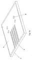
- Figs. 1a , b are a 3D perspective view and a top view of a substrate; the substrate comprises conductive trace lines and a location for receiving an optoelectronic chip;
- Fig. 1 c is a 3D perspective view of a standard Ceramic-Pin Grid Array (C-PGA) carrier with an optoelectronic device and transparent epoxy deposited in the open cavity;
- C-PGA Ceramic-Pin Grid Array
- Fig. 1d is a 3D perspective view of a custom carrier with the optoelectronic device on a separate block and a printed circuit board adjacent to the optoelectronic device;
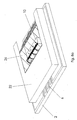
- Figs. 2a , b are a 3D perspective view and a top view of a substrate where an optoelectronic chip has been secured using electrically conductive epoxy;
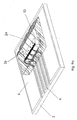
- Figs. 3a , b are a 3D perspective view and a top view of a substrate where a bump of transparent epoxy has been placed over the secured optoelectronic chip;
- Fig. 4a , b are a 3D perspective view and a top view of a substrate with a secured optoelectronic chip where the bump of epoxy has been polished over said optoelectronic chip;
- Fig. 5 is a diagram which shows a geometric determination of maximum polish height
- Figs. 6a , b a 3D perspective view and a top view of a substrate with a secured optoelectronic chip where a protection plate surrounding the optoelectronic chip has been placed;
- Figs. 7a , b are a 3D perspective view and a top view of a substrate with a secured optoelectronic chip where the protection plate surrounding the optoelectronic chip has been placed together with epoxy;
- Figs 8a , b are a 3D perspective view and a top view of a substrate with a secured optoelectronic chip where the protection plate surrounding the optoelectronic chip has been placed together with polished epoxy;
- Figs. 9a , b are a 3D perspective view and a top view of a substrate with a secured optoelectronic chip with an optional removal of the protection plate.
- Fig. 10a is a 3D perspective view of a optical ferrule over the packaged optoelectronic chip
- Fig. 10b is a 3D perspective view of a metallic layer coated over the optical ferrule and packaged optoelectronic chip;
- Fig. 10c is a 3D perspective view of a plastic protection resin (glob-top) over the metal coated optical ferrule and packaged optoelectronic chip;
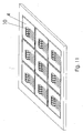
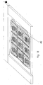
- Fig. 11 is a 3D perspective view of an example 3x3 array of substrates where optoelectronic chips have been secured and wirebonded using electrically conductive epoxy and wirebonds, respectively;
- Fig. 12 is a 3D perspective view of the 3x3 array of substrates with a raised border surrounding;
- Fig. 13 is a 3D perspective view of the 3x3 array of substrates with an optically transparent encapsulating material deposited over the entire area;
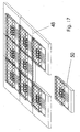
- Fig. 14 is a 3D perspective view of the screen-printing process of dragging a rigid squeegee or edge over the optically transparent encapsulating material to produce a thin, flat layer that covers the optoelectronic chips and wirebonds;
- Fig. 15 is a 3D perspective view of the 3x3 array with an opaque mask placed over the optically transparent encapsulating material;
- Fig. 16 is a 3D perspective view of several regions of hardened optically transparent encapsulating material.
- Fig. 17 is a 3D perspective view of the 3x3 array having been divided into 9 individual encapsulated packages.
- the encapsulated optical package provides a simple method of producing an optical quality flat window over the active region of an optoelectronic device.
- the optical window is created perpendicularly to the direction of light emission/detection of the optoelectronic device.
- the window is created over the chip and is co-planar with the chip.
- VCSEL vertical cavity surface emitting laser
- the optical window allows a method of alignment that eliminates several undesirable degrees of mechanical freedom.
- the flat, co-planar window restricts alignment to 2 lateral movements and one rotational movement (X, Y and ⁇ Z ). Typically, there are 6 degrees of mechanical movement (X, Y, Z, ⁇ X , ⁇ Y , ⁇ Z ).
- Electrical trace lines that extend from the encapsulated optoelectronic device to an external electrical connection, such as bond-fingers or a press-fit connector, provide the electrical access to the optoelectronic device.
- the optoelectronic device is first bonded onto the substrate using an electrically and thermally conductive epoxy.
- the exact placement of the optoelectronic chip with respect to the substrate can be done with low positional accuracy. It is one aspect of this invention that allows the subsequent alignment of optical fibers, lenses, or other optical components to the packaged optoelectronic device to be the critical alignment step for both the lateral and rotational position. Once optical fibers, lenses, or other optical components are aligned and fixed over the packaged optoelectronic device, the far-end of the optical fibers, lenses, or other optical components becomes the optical reference surface and the electrical connections on the substrate must accommodate any positional error.
- This packaging method also hermetically seals the optoelectronic chip so that it is not susceptible to humidity. Also, since the chip is encapsulated, its tolerance to mechanical vibration is greatly increased.
- the divergence angle of the light-emitting device is decreased, allowing for a better coupling efficiency.
- the substrate (2) is the mechanical support for the assembly. It carries all of the elements and is used to electrically access the optoelectronic chip.
- the chip carrier There are many possible configurations for the chip carrier. The first is to use off-the-shelf pin grid array (PGA) chip carriers that have an inner cavity where the optoelectronic is placed and outer connection pins which are plugged into the PCB as shown in Figure 1c . Transparent epoxy would be placed in the inner cavity over the optoelectronic chip and then polished flat.
- PGA pin grid array
- a second version, as shown in Figures 1 a and 1b is a more custom approach and could be based on patterning gold on an alumina substrate.
- a thin gold layer can typically be deposited on a flat aluminum oxide wafer or chip onto which the optoelectronic can be glued and wirebonded.
- the external electrical connections to this custom-made chip carrier would allow, preferably, a second set of wirebonds from the substrate to an external PCB to take up the slack for any initial misalignment of the optoelectronic device with respect to the substrate.
- a third version is another custom approach that uses PCB technology and a small form connector to create the chip carrier as shown in Figure 1d .
- the PCB (3) consists of trace lines (5) and a card-edge or similar electrical connection (7).
- the optoelectronic is placed on a metallic heat sink (9) over which the PCB is placed and bonded.
- the primary gain of this type of carrier is its adaptable geometry and its heat-sinking capabilities. The steps described below involving transparent epoxy and polishing could all be equally applied to any of these mentioned arrangements of chip packages.
- the chip carrier will be based on the second version, as shown in Figures 1a , b , described above based on the gold patterned alumina substrate.
- the Encapsulated Optical Package consists of 5 elements. The elements are described as a substrate (or carrier package), transparent epoxy, electrically conductive epoxy, wirebonds, and an optoelectronic chip.
- the custom-made alumina substrate is on the order of 1.5-cm x 1.5-cm x 0.2-cm in size.
- the top of the alumina substrate is patterned with a set of parallel gold trace lines (6) that start near the center of the substrate and end near one side of the substrate.
- the rest of the substrate, outside the trace lines is patterned with a continuous layer of gold (4) with alignment marks (8) for the placement of the optoelectronic chip.
- the gold thickness and quality is amenable to wedge or ball wirebonding.
- the trace lines are used to transmit electrical signals from the perimeter of the substrate to the middle of the substrate where the chip will be placed as shown in Figures 2a ,b.
- the optoelectronic chip (10) is placed near the middle of the substrate on a portion of the gold layer, within a reasonable distance for wirebonding from the tips of the trace lines.
- the emitting device such as a vertical cavity laser (12), or a detecting device, such as a photodetector, is oriented so that its direction of operation is normal to the substrate for vertical coupling of the light, although side-launched optoelectronic device may also be contemplated.
- the exact placement of the chip is not critical, as long as the chip can be properly wirebonded to the trace lines.
- the chip is epoxied in place using electrically conductive epoxy (16) and is then wirebonded to the trace lines.
- the wirebonds (14) are made as flat as possible so that their peaks are no more than 30-40-microns above the surface of the chip. Since the chip is higher than the trace lines, low wirebonds will be possible. For simplicity, and for when the chip has a common cathode, or anode, on its backside, the trace lines for the common, or ground, potential may be connected directly to the area below the chip as shown in Figures 2a ,b.
- a transparent epoxy is then used that will harden using time, heat, or UV-light with a sufficiently high hardness factor so that it can be polished.
- the epoxy has sufficient viscosity before being set so that it does not spread out over the surface too quickly.
- Dymax model: OP-4-20632
- Dexter model: Hysol CNB753-42
- Eques model: UV Laquer 1322 000 40045.
- the epoxy is deposited carefully over the optoelectronic chip, so not to damage the wirebonds.
- the epoxy forms a somewhat convex bump (18) over the optoelectronic chip that completely encapsulates both the chip and the wirebonds, as shown in Figures 3a ,b.
- the epoxy does not cover the distant ends of the trace lines so that the chip can still be accessed electrically.
- the whole package is then placed on a polishing machine so that the bump of epoxy faces the polishing paper.
- standard lapping and polishing techniques are applied, including progressively finer grits of polishing paper, correct timing, appropriate slurry mixtures, and a method of holding the parts in a rigid manner.
- the polishing is stopped before the wirebonds or optoelectronic chip are damaged and an optically flat window (20), that is co-planar with the surface of the optoelectronic device and chip substrate is formed.
- an optically flat window (20) that is co-planar with the surface of the optoelectronic device and chip substrate is formed.
- a thin, transparent layer of epoxy will remain over the chip as shown in Figures 4a ,b.
- max. height is equal to 760.5-microns.
- distances as low as 50-microns are also desirable to couple the maximum amount of light into optical fiber.
- an intervening step can be performed.
- the chip carrier, the chip, and the wirebonds are identical to the first example. However, before the transparent epoxy is placed over the chip, a frame or protection plate can be introduced.
- the protection plate (22) would typically have a hole or notch such that when it was placed on the chip carrier, it would surround the optoelectronic chip and the wirebonds.
- the protection plate could be made of various materials (glass, plastic, etc.) and would offer protection to the optoelectronic chip during the polishing procedure.
- the thickness of the protection plate could be chosen to be slightly higher that the optoelectronic chip and wirebonds, and be of a material that would polish less quickly than the transparent epoxy. This would help ensure that the optoelectronic chip was not damaged.
- the plate could be either removed, in some manner, or left in place.
- the plate is also nonconductive or at least insulated from the trace lines on the substrate, and allows access to the distant ends of the trace lines for electrical access to the optoelectronic chip.
- the transparent epoxy is then injected into the open hole, or notch, over the optoelectronic chip provided by the protection plate.
- Enough epoxy (24) is used to completely encapsulate the chip and form a rounded surface of epoxy that is higher than the protection plate as shown in Figures 7a ,b.
- the epoxy is then time, heat or UV cured.
- the assembly is then placed up side down on a polishing machine so that the protection plate and the epoxy face the polishing surface.
- the epoxy is polished until it is level with the protection plate and an optically flat window (26), that is co-planar with the chip and the substrate, is formed over the optoelectronic chip.
- standard lapping and polishing techniques are applied, including progressively finer grits of polishing paper, de-ionized water, correct timing, appropriate slurry mixtures, and a method of holding the parts in a rigid manner as shown in Figures 8a ,b.
- the encapsulated optical package must be placed into a useful support structure that allows access to the optical input or output and the electrical input or output.
- a standard method for sealing transparent epoxies is proposed in US patent 6,269,209 and US patent 6,075,911 , both use resin barriers over their transparent epoxies to eliminate moisture absorption.
- an optical ferrule (28) has been placed over the encapsulated optical package of Figure 8a .
- the area over the transparent epoxy where the 45-degree beveled optical fibers (30) exist has been coated with a metallic layer (32), preferably by selective masking and gold evaporation techniques, so that: 1) the transparent epoxy is protected from moisture, 2) the optoelectronic is electromagnetically shielded when the shield is grounded, and 3) a metallic mirror is formed over the beveled optical fibers to aid in optical reflection into the optical fiber.
- a metallic layer 32
- An embodiment of the desired encapsulated package that lends itself to volume manufacturability involves screen printing the optically transparent material over an array of optoelectronic chips.
- the pattern for a single package as shown in Figure 1a is essentially replicated several times in an array pattern on a larger substrate as shown in Figure 11 .
- An optoelectronic chip (10) is attached and wirebonded to the area just in front of the parallel gold trace lines (4).
- the entire large substrate is then placed in an assembly rig (36) that has slightly higher borders (38) than the substrate and the optoelectronic chip as shown in Figure 12 . If the substrate is 1-mm thick and the optoelectronic chip is 0.15-mm thick, then the border (38) should be approximately 1.25-mm thick to allow for a 0.1-mm layer over the top of the chip including the allowance for the loop height of the wedge wirebond.
- the transparent optical material (40) such as the epoxy OG142-17 from Epoxy Technology Inc.
- the transparent optical material (40) can be liberally applied over the surface of the substrate as in Figure 13 .
- Some care must be taken not to disturb the wirebonds, but this can usually be accomplished by gently pouring the epoxy around and then over the chip and wirebonds.
- the epoxy can be worked, or squeegeed, multiple times using a tool having a flat edge (42) (e.g., squeegee) until the surface has the desired flatness and is free of defects, more epoxy can be added over the area as well during the squeegee process as in Figure 14 .
- the assembly rig and substrate are covered with a mask (44) as in Figure 15 .
- the mask is typically a rigid glass plate that has opaque areas and transparent areas.
- the transparent regions of the mask are then centered over regions containing the optoelectronic chips and the opaque regions of the mask are centered over the regions where the bonding fingers are present.
- the goal is to harden the epoxy over the optoelectronic chips to create the flat optical windows (46), but leave the bonding fingers exposed to air as shown in Figure 16 .
- the unexposed epoxy can be washed away using ethanol or other gentle cleaning solutions and what remains is the flat encapsulating windows above the chips.
- the array can then be cut, diced, snapped or broken into its individual packages (50) as shown in Figure 17 .
- Two preferred methods of separating these parts are 1) using a wafer dicing saw and cutting each part out of the array, and 2) using pre-cuts or scoring trenches (48) under the substrate so that the parts can be snapped apart.
Landscapes
- Physics & Mathematics (AREA)
- General Physics & Mathematics (AREA)
- Optics & Photonics (AREA)
- Optical Couplings Of Light Guides (AREA)
- Led Device Packages (AREA)
- Structures Or Materials For Encapsulating Or Coating Semiconductor Devices Or Solid State Devices (AREA)
- Light Receiving Elements (AREA)
- Solid State Image Pick-Up Elements (AREA)
- Packages (AREA)
- Semiconductor Lasers (AREA)
Applications Claiming Priority (3)
| Application Number | Priority Date | Filing Date | Title |
|---|---|---|---|
| US62590603A | 2003-07-24 | 2003-07-24 | |
| US10/725,566 US7178235B2 (en) | 2003-12-03 | 2003-12-03 | Method of manufacturing an optoelectronic package |
| PCT/CA2004/001408 WO2005010580A1 (en) | 2003-07-24 | 2004-07-26 | Encapsulated optical package |
Publications (3)
| Publication Number | Publication Date |
|---|---|
| EP1654572A1 EP1654572A1 (en) | 2006-05-10 |
| EP1654572A4 EP1654572A4 (en) | 2009-03-25 |
| EP1654572B1 true EP1654572B1 (en) | 2012-03-14 |
Family
ID=34108155
Family Applications (1)
| Application Number | Title | Priority Date | Filing Date |
|---|---|---|---|
| EP04738016A Expired - Lifetime EP1654572B1 (en) | 2003-07-24 | 2004-07-26 | A screen-printing method of encapsulating optoelectronic chips |
Country Status (6)
| Country | Link |
|---|---|
| US (1) | US7820462B2 (https=) |
| EP (1) | EP1654572B1 (https=) |
| JP (1) | JP2006528834A (https=) |
| AT (1) | ATE549651T1 (https=) |
| CA (1) | CA2569265C (https=) |
| WO (1) | WO2005010580A1 (https=) |
Families Citing this family (11)
| Publication number | Priority date | Publication date | Assignee | Title |
|---|---|---|---|---|
| US7200295B2 (en) * | 2004-12-07 | 2007-04-03 | Reflex Photonics, Inc. | Optically enabled hybrid semiconductor package |
| US7482610B2 (en) * | 2005-01-13 | 2009-01-27 | Massachusetts Institute Of Technology | Vertical-cavity enhanced resonant thermal emitter |
| DE102005036824A1 (de) * | 2005-08-04 | 2007-03-29 | Siemens Ag | Chipmodul zum Einbau in Sensorchipkarten für fluidische Anwendungen sowie Verfahren zur Herstellung eines derartigen Chipmoduls |
| JP4699155B2 (ja) * | 2005-09-29 | 2011-06-08 | 日本電信電話株式会社 | 光モジュール |
| TWI325618B (en) * | 2007-01-02 | 2010-06-01 | Chipmos Technologies Inc | Film type package for fingerprint sensor |
| JP4553026B2 (ja) * | 2008-03-27 | 2010-09-29 | 富士ゼロックス株式会社 | 光伝送装置 |
| GB0902569D0 (en) | 2009-02-16 | 2009-04-01 | Univ Southampton | An optical device |
| JP5526738B2 (ja) * | 2009-11-27 | 2014-06-18 | 株式会社リコー | 発光装置、マルチビーム光源装置、マルチビーム走査装置及び画像形成装置 |
| JP6036463B2 (ja) * | 2013-03-26 | 2016-11-30 | 日立金属株式会社 | 光モジュール、光通信機器、および光伝送装置 |
| US20150030281A1 (en) * | 2013-07-25 | 2015-01-29 | Avago Technologies General IP (Singapore) Pte, Ltd. | Methods and apparatuses for preventing an optics system of an optical communications module from being damaged or moved out of alignment by external forces |
| US10877231B2 (en) | 2017-02-24 | 2020-12-29 | Reflex Photonics Inc. | Wirebonding for side-packaged optical engine |
Citations (1)
| Publication number | Priority date | Publication date | Assignee | Title |
|---|---|---|---|---|
| US4990208A (en) * | 1986-10-31 | 1991-02-05 | Seiko Epson Corporation, A Japanese Corporation | Method of manufacturing an optical recording medium |
Family Cites Families (20)
| Publication number | Priority date | Publication date | Assignee | Title |
|---|---|---|---|---|
| US4130343A (en) * | 1977-02-22 | 1978-12-19 | Bell Telephone Laboratories, Incorporated | Coupling arrangements between a light-emitting diode and an optical fiber waveguide and between an optical fiber waveguide and a semiconductor optical detector |
| US4819041A (en) | 1983-12-30 | 1989-04-04 | Amp Incorporated | Surface mounted integrated circuit chip package and method for making same |
| JPH02209785A (ja) * | 1989-02-09 | 1990-08-21 | Sony Corp | 光半導体装置 |
| EP0734074A1 (en) | 1990-07-16 | 1996-09-25 | Nitto Denko Corporation | Photosemiconductor device |
| JP2542746B2 (ja) * | 1991-03-04 | 1996-10-09 | ローム株式会社 | レ―ザダイオ―ド |
| US5313365A (en) | 1992-06-30 | 1994-05-17 | Motorola, Inc. | Encapsulated electronic package |
| US6054716A (en) * | 1997-01-10 | 2000-04-25 | Rohm Co., Ltd. | Semiconductor light emitting device having a protecting device |
| JP3087676B2 (ja) | 1997-02-13 | 2000-09-11 | 日本電気株式会社 | ゲル状樹脂を用いた光結合系及び実装構造 |
| US6583444B2 (en) * | 1997-02-18 | 2003-06-24 | Tessera, Inc. | Semiconductor packages having light-sensitive chips |
| JPH11119064A (ja) * | 1997-10-17 | 1999-04-30 | Fujitsu Ltd | 光伝送端末装置 |
| JP3355122B2 (ja) | 1998-01-08 | 2002-12-09 | 富士通株式会社 | 光モジュールの封止方法 |
| JP2000110176A (ja) * | 1998-10-02 | 2000-04-18 | Fujitsu Ltd | 光モジュール及びその製造方法 |
| WO2000031771A1 (en) | 1998-11-25 | 2000-06-02 | Act Micro Devices | Optoelectronic module and method of making same |
| JP4068842B2 (ja) | 1999-08-25 | 2008-03-26 | 浜松ホトニクス株式会社 | 光受信装置、並びに、その保持装置及び配置方法 |
| US6629209B1 (en) * | 1999-11-09 | 2003-09-30 | International Business Machines Corporation | Cache coherency protocol permitting sharing of a locked data granule |
| JP4045710B2 (ja) * | 1999-12-16 | 2008-02-13 | 松下電器産業株式会社 | 半導体発光装置の製造方法 |
| FR2807168B1 (fr) * | 2000-03-29 | 2002-11-29 | Commissariat Energie Atomique | Procede et dispositif d'alignement passif de fibres optiques et de composants optoelectroniques |
| US6709170B2 (en) * | 2001-01-08 | 2004-03-23 | Optical Communications Products, Inc. | Plastic encapsulation of optoelectronic devices for optical coupling |
| US6921920B2 (en) | 2001-08-31 | 2005-07-26 | Smith & Nephew, Inc. | Solid-state light source |
| US6874950B2 (en) * | 2002-12-17 | 2005-04-05 | International Business Machines Corporation | Devices and methods for side-coupling optical fibers to optoelectronic components |
-
2004
- 2004-07-26 EP EP04738016A patent/EP1654572B1/en not_active Expired - Lifetime
- 2004-07-26 WO PCT/CA2004/001408 patent/WO2005010580A1/en not_active Ceased
- 2004-07-26 JP JP2006520643A patent/JP2006528834A/ja not_active Ceased
- 2004-07-26 AT AT04738016T patent/ATE549651T1/de active
- 2004-07-26 US US11/569,751 patent/US7820462B2/en not_active Expired - Lifetime
- 2004-07-26 CA CA2569265A patent/CA2569265C/en not_active Expired - Lifetime
Patent Citations (1)
| Publication number | Priority date | Publication date | Assignee | Title |
|---|---|---|---|---|
| US4990208A (en) * | 1986-10-31 | 1991-02-05 | Seiko Epson Corporation, A Japanese Corporation | Method of manufacturing an optical recording medium |
Also Published As
| Publication number | Publication date |
|---|---|
| WO2005010580A1 (en) | 2005-02-03 |
| EP1654572A1 (en) | 2006-05-10 |
| CA2569265A1 (en) | 2005-02-03 |
| ATE549651T1 (de) | 2012-03-15 |
| JP2006528834A (ja) | 2006-12-21 |
| US7820462B2 (en) | 2010-10-26 |
| EP1654572A4 (en) | 2009-03-25 |
| US20080211048A1 (en) | 2008-09-04 |
| CA2569265C (en) | 2012-10-09 |
Similar Documents
| Publication | Publication Date | Title |
|---|---|---|
| US6932522B2 (en) | Method and apparatus for hermetically sealing photonic devices | |
| EP0987769B1 (en) | Photodiode module | |
| JP5086521B2 (ja) | 光受信機パッケージ | |
| JP4903685B2 (ja) | 集積光学システムを製造する方法 | |
| JP6162114B2 (ja) | 光電子モジュール、光電子モジュールの製造方法、ならびに光電子モジュールを備える機器およびデバイス | |
| JP3087676B2 (ja) | ゲル状樹脂を用いた光結合系及び実装構造 | |
| JP4234269B2 (ja) | 半導体装置及びその製造方法 | |
| US20040126117A1 (en) | Optical module and a method of fabricating the same | |
| JPH09129780A (ja) | Icパッケージ、光センサicパッケージおよびこれらの組立方法 | |
| EP1654572B1 (en) | A screen-printing method of encapsulating optoelectronic chips | |
| US6987619B2 (en) | Lens array package and fabrication method | |
| JP3532456B2 (ja) | 光学的信号の入出力機構を有する半導体装置 | |
| US7178235B2 (en) | Method of manufacturing an optoelectronic package | |
| JPH08264748A (ja) | 光導波路集積回路装置及びその製造方法 | |
| TW594094B (en) | Technique for protecting photonic devices in optoelectronic packages with clear overmolding | |
| US5545359A (en) | Method of making a plastic molded optoelectronic interface | |
| TWI838434B (zh) | 用於光電模組的真空注射成型的方法 | |
| JP4298856B2 (ja) | 半導体装置及びその製造方法 | |
| CN223450202U (zh) | 共封装光学装置和光电模块 | |
| WO2024105846A1 (ja) | 光素子およびその製造方法 | |
| JP4298857B2 (ja) | 半導体装置及びその製造方法 | |
| JP2024060736A (ja) | 光接続構造、光モジュール | |
| JPH11163391A (ja) | 光半導体装置 |
Legal Events
| Date | Code | Title | Description |
|---|---|---|---|
| PUAI | Public reference made under article 153(3) epc to a published international application that has entered the european phase |
Free format text: ORIGINAL CODE: 0009012 |
|
| 17P | Request for examination filed |
Effective date: 20060217 |
|
| AK | Designated contracting states |
Kind code of ref document: A1 Designated state(s): AT BE BG CH CY CZ DE DK EE ES FI FR GB GR HU IE IT LI LU MC NL PL PT RO SE SI SK TR |
|
| DAX | Request for extension of the european patent (deleted) | ||
| A4 | Supplementary search report drawn up and despatched |
Effective date: 20090220 |
|
| 17Q | First examination report despatched |
Effective date: 20090519 |
|
| GRAP | Despatch of communication of intention to grant a patent |
Free format text: ORIGINAL CODE: EPIDOSNIGR1 |
|
| RTI1 | Title (correction) |
Free format text: A SCREEN-PRINTING METHOD OF ENCAPSULATING OPTOELECTRONIC CHIPS |
|
| GRAS | Grant fee paid |
Free format text: ORIGINAL CODE: EPIDOSNIGR3 |
|
| GRAA | (expected) grant |
Free format text: ORIGINAL CODE: 0009210 |
|
| AK | Designated contracting states |
Kind code of ref document: B1 Designated state(s): AT BE BG CH CY CZ DE DK EE ES FI FR GB GR HU IE IT LI LU MC NL PL PT RO SE SI SK TR |
|
| REG | Reference to a national code |
Ref country code: GB Ref legal event code: FG4D |
|
| REG | Reference to a national code |
Ref country code: CH Ref legal event code: EP Ref country code: AT Ref legal event code: REF Ref document number: 549651 Country of ref document: AT Kind code of ref document: T Effective date: 20120315 |
|
| REG | Reference to a national code |
Ref country code: IE Ref legal event code: FG4D |
|
| 111Z | Information provided on other rights and legal means of execution |
Free format text: AT BE BG CH CY CZ DE DK EE ES FI FR GB GR HU IE IT LU MC NL PL PT RO SE SI SK TR Effective date: 20120222 |
|
| REG | Reference to a national code |
Ref country code: DE Ref legal event code: R096 Ref document number: 602004036899 Country of ref document: DE Effective date: 20120510 |
|
| REG | Reference to a national code |
Ref country code: NL Ref legal event code: VDEP Effective date: 20120314 |
|
| PG25 | Lapsed in a contracting state [announced via postgrant information from national office to epo] |
Ref country code: FI Free format text: LAPSE BECAUSE OF FAILURE TO SUBMIT A TRANSLATION OF THE DESCRIPTION OR TO PAY THE FEE WITHIN THE PRESCRIBED TIME-LIMIT Effective date: 20120314 Ref country code: GR Free format text: LAPSE BECAUSE OF FAILURE TO SUBMIT A TRANSLATION OF THE DESCRIPTION OR TO PAY THE FEE WITHIN THE PRESCRIBED TIME-LIMIT Effective date: 20120615 |
|
| REG | Reference to a national code |
Ref country code: AT Ref legal event code: MK05 Ref document number: 549651 Country of ref document: AT Kind code of ref document: T Effective date: 20120314 |
|
| PG25 | Lapsed in a contracting state [announced via postgrant information from national office to epo] |
Ref country code: CY Free format text: LAPSE BECAUSE OF FAILURE TO SUBMIT A TRANSLATION OF THE DESCRIPTION OR TO PAY THE FEE WITHIN THE PRESCRIBED TIME-LIMIT Effective date: 20120314 |
|
| PG25 | Lapsed in a contracting state [announced via postgrant information from national office to epo] |
Ref country code: CZ Free format text: LAPSE BECAUSE OF FAILURE TO SUBMIT A TRANSLATION OF THE DESCRIPTION OR TO PAY THE FEE WITHIN THE PRESCRIBED TIME-LIMIT Effective date: 20120314 Ref country code: RO Free format text: LAPSE BECAUSE OF FAILURE TO SUBMIT A TRANSLATION OF THE DESCRIPTION OR TO PAY THE FEE WITHIN THE PRESCRIBED TIME-LIMIT Effective date: 20120314 Ref country code: BE Free format text: LAPSE BECAUSE OF FAILURE TO SUBMIT A TRANSLATION OF THE DESCRIPTION OR TO PAY THE FEE WITHIN THE PRESCRIBED TIME-LIMIT Effective date: 20120314 Ref country code: SE Free format text: LAPSE BECAUSE OF FAILURE TO SUBMIT A TRANSLATION OF THE DESCRIPTION OR TO PAY THE FEE WITHIN THE PRESCRIBED TIME-LIMIT Effective date: 20120314 Ref country code: PL Free format text: LAPSE BECAUSE OF FAILURE TO SUBMIT A TRANSLATION OF THE DESCRIPTION OR TO PAY THE FEE WITHIN THE PRESCRIBED TIME-LIMIT Effective date: 20120314 Ref country code: EE Free format text: LAPSE BECAUSE OF FAILURE TO SUBMIT A TRANSLATION OF THE DESCRIPTION OR TO PAY THE FEE WITHIN THE PRESCRIBED TIME-LIMIT Effective date: 20120314 Ref country code: SI Free format text: LAPSE BECAUSE OF FAILURE TO SUBMIT A TRANSLATION OF THE DESCRIPTION OR TO PAY THE FEE WITHIN THE PRESCRIBED TIME-LIMIT Effective date: 20120314 |
|
| PG25 | Lapsed in a contracting state [announced via postgrant information from national office to epo] |
Ref country code: SK Free format text: LAPSE BECAUSE OF FAILURE TO SUBMIT A TRANSLATION OF THE DESCRIPTION OR TO PAY THE FEE WITHIN THE PRESCRIBED TIME-LIMIT Effective date: 20120314 Ref country code: PT Free format text: LAPSE BECAUSE OF FAILURE TO SUBMIT A TRANSLATION OF THE DESCRIPTION OR TO PAY THE FEE WITHIN THE PRESCRIBED TIME-LIMIT Effective date: 20120716 |
|
| PLBE | No opposition filed within time limit |
Free format text: ORIGINAL CODE: 0009261 |
|
| STAA | Information on the status of an ep patent application or granted ep patent |
Free format text: STATUS: NO OPPOSITION FILED WITHIN TIME LIMIT |
|
| PG25 | Lapsed in a contracting state [announced via postgrant information from national office to epo] |
Ref country code: DK Free format text: LAPSE BECAUSE OF FAILURE TO SUBMIT A TRANSLATION OF THE DESCRIPTION OR TO PAY THE FEE WITHIN THE PRESCRIBED TIME-LIMIT Effective date: 20120314 Ref country code: AT Free format text: LAPSE BECAUSE OF FAILURE TO SUBMIT A TRANSLATION OF THE DESCRIPTION OR TO PAY THE FEE WITHIN THE PRESCRIBED TIME-LIMIT Effective date: 20120314 Ref country code: NL Free format text: LAPSE BECAUSE OF FAILURE TO SUBMIT A TRANSLATION OF THE DESCRIPTION OR TO PAY THE FEE WITHIN THE PRESCRIBED TIME-LIMIT Effective date: 20120314 |
|
| 26N | No opposition filed |
Effective date: 20121217 |
|
| PG25 | Lapsed in a contracting state [announced via postgrant information from national office to epo] |
Ref country code: IT Free format text: LAPSE BECAUSE OF FAILURE TO SUBMIT A TRANSLATION OF THE DESCRIPTION OR TO PAY THE FEE WITHIN THE PRESCRIBED TIME-LIMIT Effective date: 20120314 Ref country code: MC Free format text: LAPSE BECAUSE OF NON-PAYMENT OF DUE FEES Effective date: 20120731 |
|
| REG | Reference to a national code |
Ref country code: CH Ref legal event code: PL |
|
| REG | Reference to a national code |
Ref country code: DE Ref legal event code: R097 Ref document number: 602004036899 Country of ref document: DE Effective date: 20121217 |
|
| PG25 | Lapsed in a contracting state [announced via postgrant information from national office to epo] |
Ref country code: CH Free format text: LAPSE BECAUSE OF NON-PAYMENT OF DUE FEES Effective date: 20120731 Ref country code: ES Free format text: LAPSE BECAUSE OF FAILURE TO SUBMIT A TRANSLATION OF THE DESCRIPTION OR TO PAY THE FEE WITHIN THE PRESCRIBED TIME-LIMIT Effective date: 20120625 Ref country code: LI Free format text: LAPSE BECAUSE OF NON-PAYMENT OF DUE FEES Effective date: 20120731 |
|
| REG | Reference to a national code |
Ref country code: IE Ref legal event code: MM4A |
|
| PG25 | Lapsed in a contracting state [announced via postgrant information from national office to epo] |
Ref country code: BG Free format text: LAPSE BECAUSE OF FAILURE TO SUBMIT A TRANSLATION OF THE DESCRIPTION OR TO PAY THE FEE WITHIN THE PRESCRIBED TIME-LIMIT Effective date: 20120614 Ref country code: IE Free format text: LAPSE BECAUSE OF NON-PAYMENT OF DUE FEES Effective date: 20120726 |
|
| PG25 | Lapsed in a contracting state [announced via postgrant information from national office to epo] |
Ref country code: TR Free format text: LAPSE BECAUSE OF FAILURE TO SUBMIT A TRANSLATION OF THE DESCRIPTION OR TO PAY THE FEE WITHIN THE PRESCRIBED TIME-LIMIT Effective date: 20120314 |
|
| PG25 | Lapsed in a contracting state [announced via postgrant information from national office to epo] |
Ref country code: LU Free format text: LAPSE BECAUSE OF NON-PAYMENT OF DUE FEES Effective date: 20120726 |
|
| PG25 | Lapsed in a contracting state [announced via postgrant information from national office to epo] |
Ref country code: HU Free format text: LAPSE BECAUSE OF FAILURE TO SUBMIT A TRANSLATION OF THE DESCRIPTION OR TO PAY THE FEE WITHIN THE PRESCRIBED TIME-LIMIT Effective date: 20040726 |
|
| REG | Reference to a national code |
Ref country code: FR Ref legal event code: PLFP Year of fee payment: 13 |
|
| REG | Reference to a national code |
Ref country code: FR Ref legal event code: PLFP Year of fee payment: 14 |
|
| PGFP | Annual fee paid to national office [announced via postgrant information from national office to epo] |
Ref country code: GB Payment date: 20170719 Year of fee payment: 14 Ref country code: DE Payment date: 20170724 Year of fee payment: 14 Ref country code: FR Payment date: 20170724 Year of fee payment: 14 |
|
| REG | Reference to a national code |
Ref country code: DE Ref legal event code: R119 Ref document number: 602004036899 Country of ref document: DE |
|
| GBPC | Gb: european patent ceased through non-payment of renewal fee |
Effective date: 20180726 |
|
| PG25 | Lapsed in a contracting state [announced via postgrant information from national office to epo] |
Ref country code: FR Free format text: LAPSE BECAUSE OF NON-PAYMENT OF DUE FEES Effective date: 20180731 Ref country code: DE Free format text: LAPSE BECAUSE OF NON-PAYMENT OF DUE FEES Effective date: 20190201 Ref country code: GB Free format text: LAPSE BECAUSE OF NON-PAYMENT OF DUE FEES Effective date: 20180726 |
|
| P01 | Opt-out of the competence of the unified patent court (upc) registered |
Effective date: 20230528 |