EP1650804A2 - Halbleiter-IC-Module, Herstellungsmethode und Verwendung - Google Patents
Halbleiter-IC-Module, Herstellungsmethode und Verwendung Download PDFInfo
- Publication number
- EP1650804A2 EP1650804A2 EP05028092A EP05028092A EP1650804A2 EP 1650804 A2 EP1650804 A2 EP 1650804A2 EP 05028092 A EP05028092 A EP 05028092A EP 05028092 A EP05028092 A EP 05028092A EP 1650804 A2 EP1650804 A2 EP 1650804A2
- Authority
- EP
- European Patent Office
- Prior art keywords
- power supply
- lsi
- package
- module
- semiconductor integrated
- Prior art date
- Legal status (The legal status is an assumption and is not a legal conclusion. Google has not performed a legal analysis and makes no representation as to the accuracy of the status listed.)
- Withdrawn
Links
Images





Classifications
-
- H—ELECTRICITY
- H05—ELECTRIC TECHNIQUES NOT OTHERWISE PROVIDED FOR
- H05K—PRINTED CIRCUITS; CASINGS OR CONSTRUCTIONAL DETAILS OF ELECTRIC APPARATUS; MANUFACTURE OF ASSEMBLAGES OF ELECTRICAL COMPONENTS
- H05K1/00—Printed circuits
- H05K1/18—Printed circuits structurally associated with non-printed electric components
- H05K1/181—Printed circuits structurally associated with non-printed electric components associated with surface mounted components
-
- H—ELECTRICITY
- H05—ELECTRIC TECHNIQUES NOT OTHERWISE PROVIDED FOR
- H05K—PRINTED CIRCUITS; CASINGS OR CONSTRUCTIONAL DETAILS OF ELECTRIC APPARATUS; MANUFACTURE OF ASSEMBLAGES OF ELECTRICAL COMPONENTS
- H05K1/00—Printed circuits
- H05K1/02—Details
- H05K1/14—Structural association of two or more printed circuits
- H05K1/141—One or more single auxiliary printed circuits mounted on a main printed circuit, e.g. modules, adapters
-
- H—ELECTRICITY
- H10—SEMICONDUCTOR DEVICES; ELECTRIC SOLID-STATE DEVICES NOT OTHERWISE PROVIDED FOR
- H10W—GENERIC PACKAGES, INTERCONNECTIONS, CONNECTORS OR OTHER CONSTRUCTIONAL DETAILS OF DEVICES COVERED BY CLASS H10
- H10W40/00—Arrangements for thermal protection or thermal control
- H10W40/20—Arrangements for cooling
- H10W40/22—Arrangements for cooling characterised by their shape, e.g. having conical or cylindrical projections
-
- H—ELECTRICITY
- H10—SEMICONDUCTOR DEVICES; ELECTRIC SOLID-STATE DEVICES NOT OTHERWISE PROVIDED FOR
- H10W—GENERIC PACKAGES, INTERCONNECTIONS, CONNECTORS OR OTHER CONSTRUCTIONAL DETAILS OF DEVICES COVERED BY CLASS H10
- H10W42/00—Arrangements for protection of devices
- H10W42/20—Arrangements for protection of devices protecting against electromagnetic or particle radiation, e.g. light, X-rays, gamma-rays or electrons
-
- H—ELECTRICITY
- H10—SEMICONDUCTOR DEVICES; ELECTRIC SOLID-STATE DEVICES NOT OTHERWISE PROVIDED FOR
- H10W—GENERIC PACKAGES, INTERCONNECTIONS, CONNECTORS OR OTHER CONSTRUCTIONAL DETAILS OF DEVICES COVERED BY CLASS H10
- H10W70/00—Package substrates; Interposers; Redistribution layers [RDL]
- H10W70/60—Insulating or insulated package substrates; Interposers; Redistribution layers
- H10W70/67—Insulating or insulated package substrates; Interposers; Redistribution layers characterised by their insulating layers or insulating parts
- H10W70/68—Shapes or dispositions thereof
-
- H—ELECTRICITY
- H10—SEMICONDUCTOR DEVICES; ELECTRIC SOLID-STATE DEVICES NOT OTHERWISE PROVIDED FOR
- H10W—GENERIC PACKAGES, INTERCONNECTIONS, CONNECTORS OR OTHER CONSTRUCTIONAL DETAILS OF DEVICES COVERED BY CLASS H10
- H10W74/00—Encapsulations, e.g. protective coatings
- H10W74/10—Encapsulations, e.g. protective coatings characterised by their shape or disposition
- H10W74/111—Encapsulations, e.g. protective coatings characterised by their shape or disposition the semiconductor body being completely enclosed
- H10W74/114—Encapsulations, e.g. protective coatings characterised by their shape or disposition the semiconductor body being completely enclosed by a substrate and the encapsulations
- H10W74/117—Encapsulations, e.g. protective coatings characterised by their shape or disposition the semiconductor body being completely enclosed by a substrate and the encapsulations the substrate having spherical bumps for external connection
-
- H—ELECTRICITY
- H10—SEMICONDUCTOR DEVICES; ELECTRIC SOLID-STATE DEVICES NOT OTHERWISE PROVIDED FOR
- H10W—GENERIC PACKAGES, INTERCONNECTIONS, CONNECTORS OR OTHER CONSTRUCTIONAL DETAILS OF DEVICES COVERED BY CLASS H10
- H10W76/00—Containers; Fillings or auxiliary members therefor; Seals
- H10W76/40—Fillings or auxiliary members in containers, e.g. centering rings
- H10W76/42—Fillings
- H10W76/47—Solid or gel fillings
-
- H—ELECTRICITY
- H10—SEMICONDUCTOR DEVICES; ELECTRIC SOLID-STATE DEVICES NOT OTHERWISE PROVIDED FOR
- H10W—GENERIC PACKAGES, INTERCONNECTIONS, CONNECTORS OR OTHER CONSTRUCTIONAL DETAILS OF DEVICES COVERED BY CLASS H10
- H10W90/00—Package configurations
-
- H—ELECTRICITY
- H05—ELECTRIC TECHNIQUES NOT OTHERWISE PROVIDED FOR
- H05K—PRINTED CIRCUITS; CASINGS OR CONSTRUCTIONAL DETAILS OF ELECTRIC APPARATUS; MANUFACTURE OF ASSEMBLAGES OF ELECTRICAL COMPONENTS
- H05K1/00—Printed circuits
- H05K1/02—Details
- H05K1/0213—Electrical arrangements not otherwise provided for
- H05K1/0254—High voltage adaptations; Electrical insulation details; Overvoltage or electrostatic discharge protection ; Arrangements for regulating voltages or for using plural voltages
- H05K1/0262—Arrangements for regulating voltages or for using plural voltages
-
- H—ELECTRICITY
- H05—ELECTRIC TECHNIQUES NOT OTHERWISE PROVIDED FOR
- H05K—PRINTED CIRCUITS; CASINGS OR CONSTRUCTIONAL DETAILS OF ELECTRIC APPARATUS; MANUFACTURE OF ASSEMBLAGES OF ELECTRICAL COMPONENTS
- H05K2201/00—Indexing scheme relating to printed circuits covered by H05K1/00
- H05K2201/10—Details of components or other objects attached to or integrated in a printed circuit board
- H05K2201/10431—Details of mounted components
- H05K2201/10507—Involving several components
- H05K2201/10515—Stacked components
-
- H—ELECTRICITY
- H05—ELECTRIC TECHNIQUES NOT OTHERWISE PROVIDED FOR
- H05K—PRINTED CIRCUITS; CASINGS OR CONSTRUCTIONAL DETAILS OF ELECTRIC APPARATUS; MANUFACTURE OF ASSEMBLAGES OF ELECTRICAL COMPONENTS
- H05K2201/00—Indexing scheme relating to printed circuits covered by H05K1/00
- H05K2201/10—Details of components or other objects attached to or integrated in a printed circuit board
- H05K2201/10431—Details of mounted components
- H05K2201/10507—Involving several components
- H05K2201/1053—Mounted components directly electrically connected to each other, i.e. not via the PCB
-
- H—ELECTRICITY
- H05—ELECTRIC TECHNIQUES NOT OTHERWISE PROVIDED FOR
- H05K—PRINTED CIRCUITS; CASINGS OR CONSTRUCTIONAL DETAILS OF ELECTRIC APPARATUS; MANUFACTURE OF ASSEMBLAGES OF ELECTRICAL COMPONENTS
- H05K2201/00—Indexing scheme relating to printed circuits covered by H05K1/00
- H05K2201/10—Details of components or other objects attached to or integrated in a printed circuit board
- H05K2201/10613—Details of electrical connections of non-printed components, e.g. special leads
- H05K2201/10621—Components characterised by their electrical contacts
- H05K2201/10689—Leaded Integrated Circuit [IC] package, e.g. dual-in-line [DIL]
-
- H—ELECTRICITY
- H05—ELECTRIC TECHNIQUES NOT OTHERWISE PROVIDED FOR
- H05K—PRINTED CIRCUITS; CASINGS OR CONSTRUCTIONAL DETAILS OF ELECTRIC APPARATUS; MANUFACTURE OF ASSEMBLAGES OF ELECTRICAL COMPONENTS
- H05K2201/00—Indexing scheme relating to printed circuits covered by H05K1/00
- H05K2201/10—Details of components or other objects attached to or integrated in a printed circuit board
- H05K2201/10613—Details of electrical connections of non-printed components, e.g. special leads
- H05K2201/10621—Components characterised by their electrical contacts
- H05K2201/10734—Ball grid array [BGA]; Bump grid array
-
- H—ELECTRICITY
- H10—SEMICONDUCTOR DEVICES; ELECTRIC SOLID-STATE DEVICES NOT OTHERWISE PROVIDED FOR
- H10W—GENERIC PACKAGES, INTERCONNECTIONS, CONNECTORS OR OTHER CONSTRUCTIONAL DETAILS OF DEVICES COVERED BY CLASS H10
- H10W40/00—Arrangements for thermal protection or thermal control
- H10W40/40—Arrangements for thermal protection or thermal control involving heat exchange by flowing fluids
- H10W40/43—Arrangements for thermal protection or thermal control involving heat exchange by flowing fluids by flowing gases, e.g. forced air cooling
-
- H—ELECTRICITY
- H10—SEMICONDUCTOR DEVICES; ELECTRIC SOLID-STATE DEVICES NOT OTHERWISE PROVIDED FOR
- H10W—GENERIC PACKAGES, INTERCONNECTIONS, CONNECTORS OR OTHER CONSTRUCTIONAL DETAILS OF DEVICES COVERED BY CLASS H10
- H10W70/00—Package substrates; Interposers; Redistribution layers [RDL]
- H10W70/40—Leadframes
-
- H—ELECTRICITY
- H10—SEMICONDUCTOR DEVICES; ELECTRIC SOLID-STATE DEVICES NOT OTHERWISE PROVIDED FOR
- H10W—GENERIC PACKAGES, INTERCONNECTIONS, CONNECTORS OR OTHER CONSTRUCTIONAL DETAILS OF DEVICES COVERED BY CLASS H10
- H10W70/00—Package substrates; Interposers; Redistribution layers [RDL]
- H10W70/60—Insulating or insulated package substrates; Interposers; Redistribution layers
-
- H—ELECTRICITY
- H10—SEMICONDUCTOR DEVICES; ELECTRIC SOLID-STATE DEVICES NOT OTHERWISE PROVIDED FOR
- H10W—GENERIC PACKAGES, INTERCONNECTIONS, CONNECTORS OR OTHER CONSTRUCTIONAL DETAILS OF DEVICES COVERED BY CLASS H10
- H10W70/00—Package substrates; Interposers; Redistribution layers [RDL]
- H10W70/60—Insulating or insulated package substrates; Interposers; Redistribution layers
- H10W70/67—Insulating or insulated package substrates; Interposers; Redistribution layers characterised by their insulating layers or insulating parts
- H10W70/68—Shapes or dispositions thereof
- H10W70/682—Shapes or dispositions thereof comprising holes having chips therein
-
- H—ELECTRICITY
- H10—SEMICONDUCTOR DEVICES; ELECTRIC SOLID-STATE DEVICES NOT OTHERWISE PROVIDED FOR
- H10W—GENERIC PACKAGES, INTERCONNECTIONS, CONNECTORS OR OTHER CONSTRUCTIONAL DETAILS OF DEVICES COVERED BY CLASS H10
- H10W70/00—Package substrates; Interposers; Redistribution layers [RDL]
- H10W70/60—Insulating or insulated package substrates; Interposers; Redistribution layers
- H10W70/67—Insulating or insulated package substrates; Interposers; Redistribution layers characterised by their insulating layers or insulating parts
- H10W70/68—Shapes or dispositions thereof
- H10W70/685—Shapes or dispositions thereof comprising multiple insulating layers
-
- H—ELECTRICITY
- H10—SEMICONDUCTOR DEVICES; ELECTRIC SOLID-STATE DEVICES NOT OTHERWISE PROVIDED FOR
- H10W—GENERIC PACKAGES, INTERCONNECTIONS, CONNECTORS OR OTHER CONSTRUCTIONAL DETAILS OF DEVICES COVERED BY CLASS H10
- H10W72/00—Interconnections or connectors in packages
- H10W72/071—Connecting or disconnecting
- H10W72/075—Connecting or disconnecting of bond wires
- H10W72/07551—Connecting or disconnecting of bond wires characterised by changes in properties of the bond wires during the connecting
- H10W72/07554—Connecting or disconnecting of bond wires characterised by changes in properties of the bond wires during the connecting changes in dispositions
-
- H—ELECTRICITY
- H10—SEMICONDUCTOR DEVICES; ELECTRIC SOLID-STATE DEVICES NOT OTHERWISE PROVIDED FOR
- H10W—GENERIC PACKAGES, INTERCONNECTIONS, CONNECTORS OR OTHER CONSTRUCTIONAL DETAILS OF DEVICES COVERED BY CLASS H10
- H10W72/00—Interconnections or connectors in packages
- H10W72/50—Bond wires
- H10W72/541—Dispositions of bond wires
- H10W72/547—Dispositions of multiple bond wires
-
- H—ELECTRICITY
- H10—SEMICONDUCTOR DEVICES; ELECTRIC SOLID-STATE DEVICES NOT OTHERWISE PROVIDED FOR
- H10W—GENERIC PACKAGES, INTERCONNECTIONS, CONNECTORS OR OTHER CONSTRUCTIONAL DETAILS OF DEVICES COVERED BY CLASS H10
- H10W74/00—Encapsulations, e.g. protective coatings
-
- H—ELECTRICITY
- H10—SEMICONDUCTOR DEVICES; ELECTRIC SOLID-STATE DEVICES NOT OTHERWISE PROVIDED FOR
- H10W—GENERIC PACKAGES, INTERCONNECTIONS, CONNECTORS OR OTHER CONSTRUCTIONAL DETAILS OF DEVICES COVERED BY CLASS H10
- H10W90/00—Package configurations
- H10W90/701—Package configurations characterised by the relative positions of pads or connectors relative to package parts
- H10W90/721—Package configurations characterised by the relative positions of pads or connectors relative to package parts of bump connectors
- H10W90/722—Package configurations characterised by the relative positions of pads or connectors relative to package parts of bump connectors between stacked chips
-
- H—ELECTRICITY
- H10—SEMICONDUCTOR DEVICES; ELECTRIC SOLID-STATE DEVICES NOT OTHERWISE PROVIDED FOR
- H10W—GENERIC PACKAGES, INTERCONNECTIONS, CONNECTORS OR OTHER CONSTRUCTIONAL DETAILS OF DEVICES COVERED BY CLASS H10
- H10W90/00—Package configurations
- H10W90/701—Package configurations characterised by the relative positions of pads or connectors relative to package parts
- H10W90/751—Package configurations characterised by the relative positions of pads or connectors relative to package parts of bond wires
- H10W90/754—Package configurations characterised by the relative positions of pads or connectors relative to package parts of bond wires between a chip and a stacked insulating package substrate, interposer or RDL
-
- H—ELECTRICITY
- H10—SEMICONDUCTOR DEVICES; ELECTRIC SOLID-STATE DEVICES NOT OTHERWISE PROVIDED FOR
- H10W—GENERIC PACKAGES, INTERCONNECTIONS, CONNECTORS OR OTHER CONSTRUCTIONAL DETAILS OF DEVICES COVERED BY CLASS H10
- H10W90/00—Package configurations
- H10W90/701—Package configurations characterised by the relative positions of pads or connectors relative to package parts
- H10W90/751—Package configurations characterised by the relative positions of pads or connectors relative to package parts of bond wires
- H10W90/756—Package configurations characterised by the relative positions of pads or connectors relative to package parts of bond wires between a chip and a stacked lead frame, conducting package substrate or heat sink
-
- Y—GENERAL TAGGING OF NEW TECHNOLOGICAL DEVELOPMENTS; GENERAL TAGGING OF CROSS-SECTIONAL TECHNOLOGIES SPANNING OVER SEVERAL SECTIONS OF THE IPC; TECHNICAL SUBJECTS COVERED BY FORMER USPC CROSS-REFERENCE ART COLLECTIONS [XRACs] AND DIGESTS
- Y02—TECHNOLOGIES OR APPLICATIONS FOR MITIGATION OR ADAPTATION AGAINST CLIMATE CHANGE
- Y02P—CLIMATE CHANGE MITIGATION TECHNOLOGIES IN THE PRODUCTION OR PROCESSING OF GOODS
- Y02P70/00—Climate change mitigation technologies in the production process for final industrial or consumer products
- Y02P70/50—Manufacturing or production processes characterised by the final manufactured product
Definitions
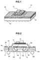
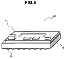
- the present invention relates to a package enclosing a semiconductor integrated circuit or a semiconductor chip and to a power supply module that supplies power to the package, and more particularly to a semiconductor integrated circuit module comprising a power supply module provided in the direction perpendicular to the surface of the package and in the vicinity thereof
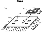
- a power supply module is mounted on a package enclosing or sealing a semiconductor integrated circuit (IC, LSI), in the direction perpendicular to the surface of the package.
- the pin arrangement of the power supply module is standardised.
- the package and the power supply module disposed in the vicinity thereof are handled as a semiconductor integrated circuit module.
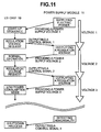
- a signal such as an input/output voltage of the power supply module is input in a voltage variation detection circuit unit provided inside a chip such as LSI.
- the power supply distance between the power supply module and a chip, such as LSI, serving as a load therefor can be shortened. Therefore, the radiation of power source noise can be reduced. Moreover, since shortening of the power supply distance decreases the resistance and inductance of the power supply line, the efficiency of the power supply unit of the power supply module is increased, the variations of the power supply voltage are reduced, and a high-speed response is made possible.
- power supply modules required for each package can be mounted on individual packages. Therefore, they can be handled as semiconductor integrated circuit modules. As a result, the number of power source types (voltage types) required for the substrate can be decreased and the mounting efficiency of the substrate is improved. Furthermore, even with the power source of one type, since the power supply module can be mounted on the upper surface of an LSI package, the mounting efficiency of the substrate is increased.
- Electromagnetic noise can be decreased, the power supply unit can operate with a high efficiency and high-speed response, and the unnecessary radiation of electromagnetic waves can be reduced.
- the emission of power source noise can be reduced because the power supply distance between the power supply module and a chip such as LSI chip serving as a load therefor can be shortened.
- Shortening the power supply distance decreases the power line resistance and inductance. Therefore, the efficiency of power supply unit of power supply module is increased, variations of power supply voltage are decreased, and a high-speed response is made possible.
- the power supply modules required for each package can be mounted on each package. Therefore, handling them as semiconductor integrated circuit modules makes it possible to reduce the number of power source types (voltage types) which are required to be on the substrate and the mounting efficiency of the substrate relating to mounting of electronic circuits other than power supply modules is increased.
- the power supply module can be mounted on the upper surface of LSI package, the mounting efficiency of the substrate is increased.
- the substrate surface and the internal power source plane can be a single surface and the substrate can be manufactured at a low cost.
- power supply module makes it possible to standardise the power supply modules and LSI packages. Therefore, power supply modules should not be designed for each LSI package, the number of design operations is decreased, and the production cost can be reduced.
Landscapes
- Engineering & Computer Science (AREA)
- Microelectronics & Electronic Packaging (AREA)
- Semiconductor Integrated Circuits (AREA)
- Shielding Devices Or Components To Electric Or Magnetic Fields (AREA)
- Cooling Or The Like Of Semiconductors Or Solid State Devices (AREA)
Applications Claiming Priority (2)
| Application Number | Priority Date | Filing Date | Title |
|---|---|---|---|
| JP2001275887A JP3944369B2 (ja) | 2001-09-12 | 2001-09-12 | 半導体集積回路モジュール及びその使用方法 |
| EP02003595A EP1294023B1 (de) | 2001-09-12 | 2002-02-15 | Halbleiter-IC-Module, Herstellungsmethode und Verwendung |
Related Parent Applications (2)
| Application Number | Title | Priority Date | Filing Date |
|---|---|---|---|
| EP02003595A Division EP1294023B1 (de) | 2001-09-12 | 2002-02-15 | Halbleiter-IC-Module, Herstellungsmethode und Verwendung |
| EP02003595.2 Division | 2002-02-15 |
Publications (2)
| Publication Number | Publication Date |
|---|---|
| EP1650804A2 true EP1650804A2 (de) | 2006-04-26 |
| EP1650804A3 EP1650804A3 (de) | 2010-09-08 |
Family
ID=19100674
Family Applications (3)
| Application Number | Title | Priority Date | Filing Date |
|---|---|---|---|
| EP05028092A Withdrawn EP1650804A3 (de) | 2001-09-12 | 2002-02-15 | Halbleiter-IC-Module, Herstellungsmethode und Verwendung |
| EP02003595A Expired - Lifetime EP1294023B1 (de) | 2001-09-12 | 2002-02-15 | Halbleiter-IC-Module, Herstellungsmethode und Verwendung |
| EP05028093A Withdrawn EP1650805A3 (de) | 2001-09-12 | 2002-02-15 | Halbleiter-IC-Module, Herstellungsmethode und Verwendung |
Family Applications After (2)
| Application Number | Title | Priority Date | Filing Date |
|---|---|---|---|
| EP02003595A Expired - Lifetime EP1294023B1 (de) | 2001-09-12 | 2002-02-15 | Halbleiter-IC-Module, Herstellungsmethode und Verwendung |
| EP05028093A Withdrawn EP1650805A3 (de) | 2001-09-12 | 2002-02-15 | Halbleiter-IC-Module, Herstellungsmethode und Verwendung |
Country Status (4)
| Country | Link |
|---|---|
| US (1) | US6777795B2 (de) |
| EP (3) | EP1650804A3 (de) |
| JP (1) | JP3944369B2 (de) |
| DE (1) | DE60227139D1 (de) |
Cited By (1)
| Publication number | Priority date | Publication date | Assignee | Title |
|---|---|---|---|---|
| DE102006033175A1 (de) * | 2006-07-18 | 2008-01-24 | Robert Bosch Gmbh | Elektronikanordnung |
Families Citing this family (11)
| Publication number | Priority date | Publication date | Assignee | Title |
|---|---|---|---|---|
| JP2004288834A (ja) * | 2003-03-20 | 2004-10-14 | Fujitsu Ltd | 電子部品の実装方法、実装構造及びパッケージ基板 |
| US7732904B2 (en) * | 2003-10-10 | 2010-06-08 | Interconnect Portfolio Llc | Multi-surface contact IC packaging structures and assemblies |
| US7652381B2 (en) | 2003-11-13 | 2010-01-26 | Interconnect Portfolio Llc | Interconnect system without through-holes |
| WO2005050708A2 (en) * | 2003-11-13 | 2005-06-02 | Silicon Pipe, Inc. | Stair step printed circuit board structures for high speed signal transmissions |
| US7250672B2 (en) * | 2003-11-13 | 2007-07-31 | International Rectifier Corporation | Dual semiconductor die package with reverse lead form |
| US7278855B2 (en) | 2004-02-09 | 2007-10-09 | Silicon Pipe, Inc | High speed, direct path, stair-step, electronic connectors with improved signal integrity characteristics and methods for their manufacture |
| TWI237882B (en) * | 2004-05-11 | 2005-08-11 | Via Tech Inc | Stacked multi-chip package |
| ATE493869T1 (de) | 2005-07-12 | 2011-01-15 | Alcatel Lucent | Verstärker mit rückkopplungsbrückenschaltung |
| US8253420B2 (en) * | 2009-12-04 | 2012-08-28 | Volterra Semiconductor Corporation | Integrated electrical circuit and test to determine the integrity of a silicon die |
| JP2014179484A (ja) * | 2013-03-15 | 2014-09-25 | Toshiba Corp | 半導体記憶装置 |
| KR102041644B1 (ko) * | 2014-01-08 | 2019-11-07 | 삼성전기주식회사 | 전력 모듈 패키지와 이의 제작방법 |
Family Cites Families (15)
| Publication number | Priority date | Publication date | Assignee | Title |
|---|---|---|---|---|
| US5444298A (en) * | 1993-02-04 | 1995-08-22 | Intel Corporation | Voltage converting integrated circuit package |
| US5444296A (en) * | 1993-11-22 | 1995-08-22 | Sun Microsystems, Inc. | Ball grid array packages for high speed applications |
| US5556811A (en) * | 1993-12-21 | 1996-09-17 | Intel Corporation | Method of optimizing operating parameters of an integrated circuit package having a voltage regulator mounted thereon |
| US5440520A (en) * | 1994-09-16 | 1995-08-08 | Intel Corporation | Integrated circuit device that selects its own supply voltage by controlling a power supply |
| JPH08279593A (ja) | 1995-04-04 | 1996-10-22 | Nec Corp | 高密度実装を可能にした半導体装置 |
| US5694297A (en) * | 1995-09-05 | 1997-12-02 | Astec International Limited | Integrated circuit mounting structure including a switching power supply |
| US5808377A (en) * | 1996-01-11 | 1998-09-15 | Intel Corporation | Power supply contention prevention circuit |
| JPH11177015A (ja) | 1997-12-11 | 1999-07-02 | Canon Inc | 半導体パッケージおよび半導体パッケージ実装用中間基板 |
| US6159765A (en) * | 1998-03-06 | 2000-12-12 | Microchip Technology, Incorporated | Integrated circuit package having interchip bonding and method therefor |
| US6181008B1 (en) * | 1998-11-12 | 2001-01-30 | Sarnoff Corporation | Integrated circuit power supply |
| JP2000349228A (ja) | 1999-06-09 | 2000-12-15 | Hitachi Ltd | 積層型半導体パッケージ |
| JP4012655B2 (ja) | 1999-08-30 | 2007-11-21 | 京セラ株式会社 | 半導体装置 |
| US6184580B1 (en) * | 1999-09-10 | 2001-02-06 | Siliconware Precision Industries Co., Ltd. | Ball grid array package with conductive leads |
| US6394175B1 (en) * | 2000-01-13 | 2002-05-28 | Lucent Technologies Inc. | Top mounted cooling device using heat pipes |
| KR100370231B1 (ko) * | 2000-06-13 | 2003-01-29 | 페어차일드코리아반도체 주식회사 | 리드프레임의 배면에 직접 부착되는 절연방열판을구비하는 전력 모듈 패키지 |
-
2001
- 2001-09-12 JP JP2001275887A patent/JP3944369B2/ja not_active Expired - Fee Related
-
2002
- 2002-02-15 EP EP05028092A patent/EP1650804A3/de not_active Withdrawn
- 2002-02-15 DE DE60227139T patent/DE60227139D1/de not_active Expired - Lifetime
- 2002-02-15 EP EP02003595A patent/EP1294023B1/de not_active Expired - Lifetime
- 2002-02-15 EP EP05028093A patent/EP1650805A3/de not_active Withdrawn
- 2002-02-20 US US10/077,779 patent/US6777795B2/en not_active Expired - Lifetime
Cited By (1)
| Publication number | Priority date | Publication date | Assignee | Title |
|---|---|---|---|---|
| DE102006033175A1 (de) * | 2006-07-18 | 2008-01-24 | Robert Bosch Gmbh | Elektronikanordnung |
Also Published As
| Publication number | Publication date |
|---|---|
| EP1650804A3 (de) | 2010-09-08 |
| JP3944369B2 (ja) | 2007-07-11 |
| EP1650805A2 (de) | 2006-04-26 |
| US6777795B2 (en) | 2004-08-17 |
| EP1650805A3 (de) | 2010-09-08 |
| JP2003086754A (ja) | 2003-03-20 |
| US20030047800A1 (en) | 2003-03-13 |
| EP1294023A2 (de) | 2003-03-19 |
| DE60227139D1 (de) | 2008-07-31 |
| EP1294023A3 (de) | 2004-12-29 |
| EP1294023B1 (de) | 2008-06-18 |
Similar Documents
| Publication | Publication Date | Title |
|---|---|---|
| US6346743B1 (en) | Embedded capacitor assembly in a package | |
| US7538441B2 (en) | Chip with power and signal pads connected to power and signal lines on substrate | |
| US7215016B2 (en) | Multi-chips stacked package | |
| US5847951A (en) | Method and apparatus for voltage regulation within an integrated circuit package | |
| US6534879B2 (en) | Semiconductor chip and semiconductor device having the chip | |
| US5789816A (en) | Multiple-chip integrated circuit package including a dummy chip | |
| US6528872B2 (en) | Packaging structure for ball grid array | |
| EP1294023B1 (de) | Halbleiter-IC-Module, Herstellungsmethode und Verwendung | |
| JPH09148476A (ja) | Bga型半導体装置およびそのための部品および電子装置 | |
| US20090236709A1 (en) | Semiconductor chip package | |
| JP7362380B2 (ja) | 配線基板及び半導体装置 | |
| US20220068734A1 (en) | Semiconductor device | |
| JPH09223861A (ja) | 半導体集積回路及びプリント配線基板 | |
| US20040113252A1 (en) | Partially populated ball grid design to accommodate landing pads close to the die | |
| US8362614B2 (en) | Fine pitch grid array type semiconductor device | |
| US20050073050A1 (en) | BGA package and printed circuit board for supporting the package | |
| CN112768425B (zh) | 一种多芯片模块 | |
| US6281580B1 (en) | LSI package and inner lead wiring method for same | |
| US20120025898A1 (en) | Circuit Device | |
| KR102830332B1 (ko) | 반도체 패키지 | |
| CN100565861C (zh) | 半导体器件及其制造方法 | |
| US7187065B2 (en) | Semiconductor device and semiconductor device unit | |
| JPH05226567A (ja) | 半導体パッケージ | |
| JPH04284662A (ja) | 半導体モジュールの実装構造 | |
| JPH06120404A (ja) | 電子部品搭載用基板 |
Legal Events
| Date | Code | Title | Description |
|---|---|---|---|
| PUAI | Public reference made under article 153(3) epc to a published international application that has entered the european phase |
Free format text: ORIGINAL CODE: 0009012 |
|
| AC | Divisional application: reference to earlier application |
Ref document number: 1294023 Country of ref document: EP Kind code of ref document: P |
|
| AK | Designated contracting states |
Kind code of ref document: A2 Designated state(s): DE FR GB |
|
| PUAL | Search report despatched |
Free format text: ORIGINAL CODE: 0009013 |
|
| AK | Designated contracting states |
Kind code of ref document: A3 Designated state(s): DE FR GB |
|
| AKY | No designation fees paid | ||
| STAA | Information on the status of an ep patent application or granted ep patent |
Free format text: STATUS: THE APPLICATION IS DEEMED TO BE WITHDRAWN |
|
| 18D | Application deemed to be withdrawn |
Effective date: 20110309 |