EP1650802A2 - Halbleiterkontrollanordnung und ihre Herstellung - Google Patents
Halbleiterkontrollanordnung und ihre Herstellung Download PDFInfo
- Publication number
- EP1650802A2 EP1650802A2 EP05021359A EP05021359A EP1650802A2 EP 1650802 A2 EP1650802 A2 EP 1650802A2 EP 05021359 A EP05021359 A EP 05021359A EP 05021359 A EP05021359 A EP 05021359A EP 1650802 A2 EP1650802 A2 EP 1650802A2
- Authority
- EP
- European Patent Office
- Prior art keywords
- opening
- semiconductor substrate
- forming
- layer
- monitoring
- Prior art date
- Legal status (The legal status is an assumption and is not a legal conclusion. Google has not performed a legal analysis and makes no representation as to the accuracy of the status listed.)
- Withdrawn
Links
Images


Classifications
-
- H—ELECTRICITY
- H10—SEMICONDUCTOR DEVICES; ELECTRIC SOLID-STATE DEVICES NOT OTHERWISE PROVIDED FOR
- H10W—GENERIC PACKAGES, INTERCONNECTIONS, CONNECTORS OR OTHER CONSTRUCTIONAL DETAILS OF DEVICES COVERED BY CLASS H10
- H10W76/00—Containers; Fillings or auxiliary members therefor; Seals
- H10W76/10—Containers or parts thereof
- H10W76/12—Containers or parts thereof characterised by their shape
- H10W76/15—Containers comprising an insulating or insulated base
- H10W76/153—Containers comprising an insulating or insulated base having interconnections in passages through the insulating or insulated base
-
- H—ELECTRICITY
- H10—SEMICONDUCTOR DEVICES; ELECTRIC SOLID-STATE DEVICES NOT OTHERWISE PROVIDED FOR
- H10P—GENERIC PROCESSES OR APPARATUS FOR THE MANUFACTURE OR TREATMENT OF DEVICES COVERED BY CLASS H10
- H10P74/00—Testing or measuring during manufacture or treatment of wafers, substrates or devices
- H10P74/27—Structural arrangements therefor
- H10P74/277—Circuits for electrically characterising or monitoring manufacturing processes, e.g. circuits in tested chips or circuits in testing wafers
-
- H—ELECTRICITY
- H10—SEMICONDUCTOR DEVICES; ELECTRIC SOLID-STATE DEVICES NOT OTHERWISE PROVIDED FOR
- H10W—GENERIC PACKAGES, INTERCONNECTIONS, CONNECTORS OR OTHER CONSTRUCTIONAL DETAILS OF DEVICES COVERED BY CLASS H10
- H10W20/00—Interconnections in chips, wafers or substrates
- H10W20/01—Manufacture or treatment
- H10W20/021—Manufacture or treatment of interconnections within wafers or substrates
- H10W20/023—Manufacture or treatment of interconnections within wafers or substrates the interconnections being through-semiconductor vias
-
- H—ELECTRICITY
- H10—SEMICONDUCTOR DEVICES; ELECTRIC SOLID-STATE DEVICES NOT OTHERWISE PROVIDED FOR
- H10W—GENERIC PACKAGES, INTERCONNECTIONS, CONNECTORS OR OTHER CONSTRUCTIONAL DETAILS OF DEVICES COVERED BY CLASS H10
- H10W20/00—Interconnections in chips, wafers or substrates
- H10W20/01—Manufacture or treatment
- H10W20/021—Manufacture or treatment of interconnections within wafers or substrates
- H10W20/023—Manufacture or treatment of interconnections within wafers or substrates the interconnections being through-semiconductor vias
- H10W20/0234—Manufacture or treatment of interconnections within wafers or substrates the interconnections being through-semiconductor vias comprising etching via holes that stop on pads or on electrodes
-
- H—ELECTRICITY
- H10—SEMICONDUCTOR DEVICES; ELECTRIC SOLID-STATE DEVICES NOT OTHERWISE PROVIDED FOR
- H10W—GENERIC PACKAGES, INTERCONNECTIONS, CONNECTORS OR OTHER CONSTRUCTIONAL DETAILS OF DEVICES COVERED BY CLASS H10
- H10W20/00—Interconnections in chips, wafers or substrates
- H10W20/01—Manufacture or treatment
- H10W20/021—Manufacture or treatment of interconnections within wafers or substrates
- H10W20/023—Manufacture or treatment of interconnections within wafers or substrates the interconnections being through-semiconductor vias
- H10W20/0242—Manufacture or treatment of interconnections within wafers or substrates the interconnections being through-semiconductor vias comprising etching via holes from the back sides of the chips, wafers or substrates
Definitions
- This invention relates to a semiconductor device having a metal layer formed on a semiconductor substrate, an opening penetrating through the semiconductor substrate to expose the metal layer and a wiring that is connected with the metal layer through the opening and its manufacturing method. Specifically this invention relates to a technology to monitor a result of the formation of the opening.
- a CSP Chip Size Package
- the CSP means a small package having about the same outside dimensions as those of a semiconductor die packaged in it.
- a BGA (Ball Grid Array) type semiconductor device has been known as a kind of CSP.
- a plurality of ball-shaped conductive terminals made of metal such as solder is arrayed in a grid pattern on one principal surface of a package of the BGA type semiconductor device and is electrically connected with the semiconductor die mounted on the other side of the package.
- the semiconductor die When the BGA type semiconductor device is mounted on electronic equipment, the semiconductor die is electrically connected with an external circuit on a printed circuit board by compression bonding of the conductive terminals to wiring patterns on the printed circuit board.
- Such a BGA type semiconductor device has advantages in providing a large number of conductive terminals and in reducing size over other CSP type semiconductor devices such as an SOP (Small Outline Package) and a QFP (Quad Flat Package), which have lead pins protruding from their sides.
- the BGA type semiconductor device is used as an image sensor chip for a digital camera incorporated into a mobile telephone, for example.
- An example of the BGA type semiconductor device includes a supporting member made of a glass, for example, attached to one of, or both of principal surfaces of the semiconductor die. Further description on the technologies mentioned above is provided in Japanese Patent Application Publication No. 2003-309221, for example.
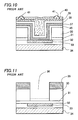
- Figs. 8 through 10 are cross-sectional views showing the manufacturing method of the BGA type semiconductor device, that is applicable to an image sensor chip, according to a conventional art.
- a pad electrode 32 that is a metal layer primarily composed of aluminum, is formed on a front surface of a semiconductor substrate 30 through an insulation layer 31 made of a silicon oxide film or a silicon nitride film, as shown in Fig. 8. Then a supporting member 34 made of glass, for example, is bonded to the semiconductor substrate 30 having the pad electrode 32 through an adhesive material 33 made of an epoxy resin layer.
- a photoresist layer 35 having an opening at a location corresponding to the pad electrode 32 is formed on a back surface of the semiconductor substrate 30.
- Plasma-etching is performed on the semiconductor substrate 30 with etching gas composed of SF 6 and O 2 , for example, using the photoresist layer 35 as a mask, and further etching is performed on the insulation layer 31 to form an opening 36 extending from the back surface of the semiconductor substrate 30 to the pad electrode 32, as shown in Fig. 9.
- a barrier layer 37 is formed on the entire surface, as shown in Fig. 10.
- a seed layer 38 for plating is formed on the barrier layer 37 and a wiring layer 39 made of copper (Cu), for example, is formed on the seed layer 38 by plating.
- a protection layer 40 is formed on the wiring layer 39, openings are formed in predetermined locations in the protection layer 40 and conductive terminals 41, that make contact with the wiring layer 39, are formed in the openings.
- a BGA type semiconductor device in which the pad electrode 32 and the conductive terminal 41 are electrically connected, is formed as described above.
- the shape of the opening 36 that is actually formed can not be recognized after the opening 36 is completed as described above, unless the semiconductor wafer is cut and a cross-section of the cut wafer is observed. That is, since the opening 36 is formed from the back surface of the opaque semiconductor substrate 30 so as to expose the pad electrode formed on the front surface of the semiconductor substrate 30 through the insulation layer 31, it is necessary to observe the opening 36 from a transparent supporting member 34 side of the semiconductor substrate 30, when the observation of the opening 36 is to be made through a microscope. When observed from the direction of the supporting member 34, however, the opening 36 is not visible because of the existence of the pad electrode 32 that is the metal layer.
- the opening size at the bottom end of the opening 36 may become too large because of the over-etching. Also, it is not possible to measure an aperture of the opening 36 visually.
- the invention provides a semiconductor wafer ready for separation into individual dice.
- the wafer includes a semiconductor substrate having a first opening, a metal layer disposed on a first surface of the semiconductor substrate, a wiring layer disposed on a second surface of the semiconductor substrate and extending into the first opening to be electrically connected with the metal layer, and a monitoring portion that is a second opening formed in the semiconductor substrate and configured to provide clear view into the second opening.
- the invention also provides a method of manufacturing a semiconductor device.
- the method includes providing a semiconductor substrate, forming a metal layer on a first surface of the semiconductor substrate, forming for a second surface of the semiconductor substrate a first opening in the semiconductor substrate to expose the metal layer, forming a second opening in the semiconductor substrate, forming a wiring layer on the second surface that is connected with the metal layer through the first opening, and viewing the second opening from a side of the first surface.
- the invention further provides a semiconductor device that includes a semiconductor substrate having a first opening, a metal layer disposed on a first surface of the semiconductor substrate, a wiring layer disposed on a second surface of the semiconductor substrate and extending into the first opening to be electrically connected with the metal layer, and a monitoring portion that is a second opening formed in the semiconductor substrate and configured to provide clear view into the second opening.
- the result of the formation of the first opening can be judged by observing the result of the formation of the monitoring opening, without cutting the wafer and observing the cross-section of the cut wafer as in the conventional art.
- the invention has realized that a recognized proper formation of the monitoring opening can assure that the first opening is proper formed, too, as a consequence that it is formed under the same process conditions as the monitoring opening.
- a main functionality of the monitoring opening is to allow for an unobstructed view into it, in particular to be recognizable from a side of the first surface.
- the invention does allow for an easy visual inspection of the result of the formation of the openings.
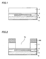
- a pad electrode 3 made of a metal layer primarily composed of aluminum is formed on a front surface of a semiconductor substrate 1 through an insulation layer 2 made of a silicon oxide film or a silicon nitride film, as shown in Fig. 1.
- a supporting member 5 made of a glass substrate is bonded to the front surface of the semiconductor substrate 1 having the pad electrode 3 through an adhesive material 4 made of an epoxy resin layer.
- the silicon wafer in this embodiment is divided into individual silicon dice to form CCD (Charge Coupled Device) image sensor chips, for example. Because the CCD in the front surface of the silicon die needs to receive external light, the supporting member 5 is required to be made of a transparent substrate such as the glass substrate or a semi-transparent substrate.
- the supporting member 5 may be an opaque substrate when the silicon die does not receive or transmit light.
- the opaque substrate is not suitable in the case where the opening 36 is observed from the supporting member 34 side, as in the conventional art.
- the opaque substrate may be used when a monitoring opening 6b, that will be described later, is observed after forming the monitoring opening 6b and removing the supporting member 5.
- this monitoring opening 6b may also be formed in the semiconductor substrate 1 to which the supporting member 5 is not bonded.
- the supporting member 5 is not limited to the glass substrate and may be made of a plastic plate or a tape-shaped material.
- the pad electrode 3 may be made of a metal other than aluminum, such as copper (Cu) or copper alloy.
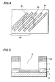
- a photoresist layer PR that has an opening at a location corresponding to the pad electrode 3 is formed on a back surface of the semiconductor substrate 1.
- An opening 6a is formed in the semiconductor substrate 1 by plasma-etching the semiconductor substrate 1 using at least SF 6 and O 2 as etching gas and the photoresist layer PR as a mask, as shown in Fig. 2.
- an opening 6b is also formed at a location of the semiconductor substrate 1 that corresponds to a scribe line, as shown in Fig. 3A.
- the opening 6b corresponds to the monitoring opening of this embodiment (hereafter referred to as the monitoring opening 6b).
- the formation of the monitoring opening 6b can be recognized by observing the monitoring opening 6b from a bottom side of Fig. 3A using an optical microscope. The recognized proper formation of the monitoring opening 6b assures the proper formation of the opening 6a which is formed under the same process conditions as the monitoring opening 6b and is not visually recognizable after the completion of the device.
- a plurality of patterned metal layers 3a may be disposed at equal spaces under the monitoring opening 6b, as shown in Fig. 3B. Measuring an aperture of the monitoring opening 6b is made possible by forming a monitoring pattern 50 made of the plurality of patterned metal layers 3a so as to overlap the monitoring opening 6b.
- the monitoring pattern 50 is made of rectangular-patterned metal layers 3a of a width of 5 ⁇ m arrayed with a constant spacing of 5 ⁇ m.
- the visual observation reveals the incomplete removal of the semiconductor portion in the opening 6a or the over-etched opening 36 at its bottom end.
- the patterned metal layers 3a it is made possible to measure the aperture of the opening 36 after the etching, without cutting the wafer and observing its cross-section as in the conventional art.
- the monitoring opening 6b is formed in the scribe line in the embodiment, it may be formed in an unused space in the semiconductor die. In this case, the monitoring pattern 50 may be disposed at a matching location with the monitoring opening 6b.
- monitoring pattern 50 is not limited to be rectangular. Each of various shapes of monitoring patterns 50 such as circular, cruciform and rhombic in shape may be formed in the scribe line or in the semiconductor die.
- the aperture of the monitoring opening 6b is not necessarily equal to the aperture of the opening 6a.
- the result of formation of the opening 6a may be judged by observing the result of formation of the monitoring opening 6b having a different size of aperture from that of the opening 6a. Furthermore, the result of formation of the opening 6a may be judged by forming and observing a plurality of monitoring openings 6b having various sizes of apertures. Forming the plurality of monitoring openings 6b having various sizes of apertures enables judging results of formation of various patterns of openings 6a in accordance with actual patterning in the semiconductor device and improving workability of the observation.
- an insulation layer 7 made of a silicon oxide film is formed on the back surface of the semiconductor substrate 1 including the inside of the opening 6.
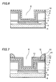
- a barrier layer 8 is formed on the entire surface, as shown in Fig. 6.
- the barrier layer 8 is preferably made of a titanium nitride (TiN) layer, for example.
- the barrier layer 8 may be made of other refractory metal or its compound such as TiW, Ta or TaN, or stacked layers of such materials.
- a seed layer 9 (a Cu layer, for example) for plating is formed on the barrier layer 8 and a wiring layer 10 made of copper (Cu), for example, is formed on the seed layer 9 by plating.
- a protection layer 11 is formed on the wiring layer 10, openings 12 are formed in the protection layer 11 at predetermined locations, a nickel (Ni) layer 13 and a gold (Au) layer 14 are formed on exposed portions of the wiring layer 10 and conductive terminals 15 connected with the wiring layer 10 through the Ni layer 13 and the Au layer 14 are formed by screen printing, as shown in Fig. 7.
- the protection layer 11 is not limited to the photoresist layer and the conductive terminals 15 are not limited to the conductive terminals 15 made of solder as described in the embodiment.
- a BGA type semiconductor device in which the pad electrode 3 and the conductive terminal 15 are electrically connected, is formed as described above.
- the wiring layer 10 is made by plating as described.
- the wiring layer 10 may be made by a method other than the plating, without forming the seed layer 9, for example. It may be made by sputtering of aluminum or aluminum alloy, for example.
- the device of this embodiment includes conductive terminals 15, as described.
- the structures of the embodiment is applicable to a semiconductor device not having the conductive terminals 15 such as an LGA (Land Grid Array) type semiconductor device, as long as the opening 6 penetrating through the semiconductor substrate 1 is formed.
- LGA Land Grid Array
- the result of the formation of the opening can be judged by observing the result of the formation of the monitoring opening in this embodiment, without cutting the wafer and observing the cross-section of the cut wafer as in the conventional art.
- the result of the formation of the monitoring opening can be easily observed by forming the monitoring opening in the scribe line and not disposing the metal layer under the monitoring opening.
- the aperture of the opening can be easily judged by forming the rectangular patters under the monitoring opening that are made of the same layer as the metal layer.
Landscapes
- Internal Circuitry In Semiconductor Integrated Circuit Devices (AREA)
- Testing Or Measuring Of Semiconductors Or The Like (AREA)
Applications Claiming Priority (1)
| Application Number | Priority Date | Filing Date | Title |
|---|---|---|---|
| JP2004285030 | 2004-09-29 |
Publications (2)
| Publication Number | Publication Date |
|---|---|
| EP1650802A2 true EP1650802A2 (de) | 2006-04-26 |
| EP1650802A3 EP1650802A3 (de) | 2009-07-15 |
Family
ID=35064727
Family Applications (1)
| Application Number | Title | Priority Date | Filing Date |
|---|---|---|---|
| EP05021359A Withdrawn EP1650802A3 (de) | 2004-09-29 | 2005-09-29 | Halbleiterkontrollanordnung und ihre Herstellung |
Country Status (5)
| Country | Link |
|---|---|
| US (2) | US7256420B2 (de) |
| EP (1) | EP1650802A3 (de) |
| KR (1) | KR100699384B1 (de) |
| CN (1) | CN100470766C (de) |
| TW (1) | TWI267183B (de) |
Cited By (1)
| Publication number | Priority date | Publication date | Assignee | Title |
|---|---|---|---|---|
| CN100587909C (zh) * | 2006-08-03 | 2010-02-03 | 国际商业机器公司 | 防止芯片中的背面微裂纹向其正面扩展的方法和芯片 |
Families Citing this family (15)
| Publication number | Priority date | Publication date | Assignee | Title |
|---|---|---|---|---|
| US10224224B2 (en) | 2017-03-10 | 2019-03-05 | Micromaterials, LLC | High pressure wafer processing systems and related methods |
| US10622214B2 (en) | 2017-05-25 | 2020-04-14 | Applied Materials, Inc. | Tungsten defluorination by high pressure treatment |
| US10388533B2 (en) * | 2017-06-16 | 2019-08-20 | Applied Materials, Inc. | Process integration method to tune resistivity of nickel silicide |
| US11276727B1 (en) * | 2017-06-19 | 2022-03-15 | Rigetti & Co, Llc | Superconducting vias for routing electrical signals through substrates and their methods of manufacture |
| US10276411B2 (en) | 2017-08-18 | 2019-04-30 | Applied Materials, Inc. | High pressure and high temperature anneal chamber |
| JP6947914B2 (ja) | 2017-08-18 | 2021-10-13 | アプライド マテリアルズ インコーポレイテッドApplied Materials,Incorporated | 高圧高温下のアニールチャンバ |
| KR102585074B1 (ko) | 2017-11-11 | 2023-10-04 | 마이크로머티어리얼즈 엘엘씨 | 고압 프로세싱 챔버를 위한 가스 전달 시스템 |
| JP2021503714A (ja) | 2017-11-17 | 2021-02-12 | アプライド マテリアルズ インコーポレイテッドApplied Materials,Incorporated | 高圧処理システムのためのコンデンサシステム |
| CN111902929B (zh) | 2018-03-09 | 2025-09-19 | 应用材料公司 | 用于含金属材料的高压退火处理 |
| US10916433B2 (en) | 2018-04-06 | 2021-02-09 | Applied Materials, Inc. | Methods of forming metal silicide layers and metal silicide layers formed therefrom |
| US10950429B2 (en) | 2018-05-08 | 2021-03-16 | Applied Materials, Inc. | Methods of forming amorphous carbon hard mask layers and hard mask layers formed therefrom |
| US10748783B2 (en) | 2018-07-25 | 2020-08-18 | Applied Materials, Inc. | Gas delivery module |
| WO2020117462A1 (en) | 2018-12-07 | 2020-06-11 | Applied Materials, Inc. | Semiconductor processing system |
| CN112310043B (zh) * | 2019-08-02 | 2022-08-30 | 联芯集成电路制造(厦门)有限公司 | 半导体结构及其缺陷检测方法 |
| US11901222B2 (en) | 2020-02-17 | 2024-02-13 | Applied Materials, Inc. | Multi-step process for flowable gap-fill film |
Family Cites Families (8)
| Publication number | Priority date | Publication date | Assignee | Title |
|---|---|---|---|---|
| US5618752A (en) * | 1995-06-05 | 1997-04-08 | Harris Corporation | Method of fabrication of surface mountable integrated circuits |
| JP2967755B2 (ja) | 1997-04-17 | 1999-10-25 | 日本電気株式会社 | 半導体装置の製造方法 |
| JPH11204525A (ja) | 1998-01-14 | 1999-07-30 | Seiko Epson Corp | 半導体装置の製造方法 |
| KR20030058309A (ko) | 2001-12-31 | 2003-07-07 | 주식회사 하이닉스반도체 | 반도체 소자 제조 방법 |
| JP4212293B2 (ja) | 2002-04-15 | 2009-01-21 | 三洋電機株式会社 | 半導体装置の製造方法 |
| TWI232560B (en) | 2002-04-23 | 2005-05-11 | Sanyo Electric Co | Semiconductor device and its manufacture |
| TWI229435B (en) * | 2002-06-18 | 2005-03-11 | Sanyo Electric Co | Manufacture of semiconductor device |
| TWI227550B (en) * | 2002-10-30 | 2005-02-01 | Sanyo Electric Co | Semiconductor device manufacturing method |
-
2005
- 2005-09-21 TW TW094132615A patent/TWI267183B/zh active
- 2005-09-27 CN CNB2005101070318A patent/CN100470766C/zh not_active Expired - Fee Related
- 2005-09-28 US US11/236,847 patent/US7256420B2/en not_active Expired - Lifetime
- 2005-09-28 KR KR1020050090408A patent/KR100699384B1/ko not_active Expired - Fee Related
- 2005-09-29 EP EP05021359A patent/EP1650802A3/de not_active Withdrawn
-
2007
- 2007-07-02 US US11/822,122 patent/US7820548B2/en active Active
Cited By (1)
| Publication number | Priority date | Publication date | Assignee | Title |
|---|---|---|---|---|
| CN100587909C (zh) * | 2006-08-03 | 2010-02-03 | 国际商业机器公司 | 防止芯片中的背面微裂纹向其正面扩展的方法和芯片 |
Also Published As
| Publication number | Publication date |
|---|---|
| CN100470766C (zh) | 2009-03-18 |
| EP1650802A3 (de) | 2009-07-15 |
| US20070254471A1 (en) | 2007-11-01 |
| US7820548B2 (en) | 2010-10-26 |
| KR100699384B1 (ko) | 2007-03-26 |
| US7256420B2 (en) | 2007-08-14 |
| TWI267183B (en) | 2006-11-21 |
| CN1755917A (zh) | 2006-04-05 |
| KR20060051744A (ko) | 2006-05-19 |
| TW200618244A (en) | 2006-06-01 |
| US20060073696A1 (en) | 2006-04-06 |
Similar Documents
| Publication | Publication Date | Title |
|---|---|---|
| US7820548B2 (en) | Semiconductor device and manufacturing method thereof | |
| US7382037B2 (en) | Semiconductor device with a peeling prevention layer | |
| CN100382304C (zh) | 半导体装置及其制造方法 | |
| EP1653509A2 (de) | Halbleitervorrichtung und Verfahren zu Ihrer Herstellung | |
| US7508072B2 (en) | Semiconductor device with pad electrode for testing and manufacturing method of the same | |
| US20050269696A1 (en) | Semiconductor device and manufacturing method of the same | |
| US7241679B2 (en) | Method of manufacturing semiconductor device | |
| JP2005142186A (ja) | 半導体装置およびその製造方法 | |
| CN101083241A (zh) | 半导体装置及其制造方法 | |
| EP1686622A2 (de) | Halbleitervorrichtung und Verfahren zu Ihrer Herstellung | |
| EP1748485A2 (de) | Halbleiterbauelement und Verfahren zu dessen Herstellung | |
| US7397134B2 (en) | Semiconductor device mounted on and electrically connected to circuit board | |
| JP4446793B2 (ja) | 半導体装置およびその製造方法 | |
| EP1622197A2 (de) | Verfahren zur Herstellung einer Halbleiteranordnung | |
| JP5238985B2 (ja) | 半導体装置の製造方法 | |
| US7511320B2 (en) | Semiconductor device and manufacturing method of the same | |
| US7812465B2 (en) | Semiconductor chip having alignment mark and method of manufacturing the same | |
| JP4936695B2 (ja) | 半導体装置及びその製造方法 | |
| JP2010016395A5 (de) | ||
| JP2004006835A (ja) | 半導体装置及びその製造方法 | |
| JP4401330B2 (ja) | 半導体装置及びその製造方法 | |
| JP2004327748A (ja) | 半導体装置及びその製造方法 | |
| JP2006049592A (ja) | 半導体装置の製造方法 |
Legal Events
| Date | Code | Title | Description |
|---|---|---|---|
| PUAI | Public reference made under article 153(3) epc to a published international application that has entered the european phase |
Free format text: ORIGINAL CODE: 0009012 |
|
| AK | Designated contracting states |
Kind code of ref document: A2 Designated state(s): AT BE BG CH CY CZ DE DK EE ES FI FR GB GR HU IE IS IT LI LT LU LV MC NL PL PT RO SE SI SK TR |
|
| AX | Request for extension of the european patent |
Extension state: AL BA HR MK YU |
|
| PUAL | Search report despatched |
Free format text: ORIGINAL CODE: 0009013 |
|
| AK | Designated contracting states |
Kind code of ref document: A3 Designated state(s): AT BE BG CH CY CZ DE DK EE ES FI FR GB GR HU IE IS IT LI LT LU LV MC NL PL PT RO SE SI SK TR |
|
| AX | Request for extension of the european patent |
Extension state: AL BA HR MK YU |
|
| 17P | Request for examination filed |
Effective date: 20100114 |
|
| AKX | Designation fees paid |
Designated state(s): DE FI FR GB |
|
| 17Q | First examination report despatched |
Effective date: 20100312 |
|
| STAA | Information on the status of an ep patent application or granted ep patent |
Free format text: STATUS: THE APPLICATION IS DEEMED TO BE WITHDRAWN |
|
| 18D | Application deemed to be withdrawn |
Effective date: 20150313 |