EP1650796A2 - Procédé de prise de contact sur une région d'un circuit intégré, en particulier sur les électrodes d'un transistor - Google Patents
Procédé de prise de contact sur une région d'un circuit intégré, en particulier sur les électrodes d'un transistor Download PDFInfo
- Publication number
- EP1650796A2 EP1650796A2 EP05292061A EP05292061A EP1650796A2 EP 1650796 A2 EP1650796 A2 EP 1650796A2 EP 05292061 A EP05292061 A EP 05292061A EP 05292061 A EP05292061 A EP 05292061A EP 1650796 A2 EP1650796 A2 EP 1650796A2
- Authority
- EP
- European Patent Office
- Prior art keywords
- region
- zone
- integrated circuit
- orifice
- transistor
- Prior art date
- Legal status (The legal status is an assumption and is not a legal conclusion. Google has not performed a legal analysis and makes no representation as to the accuracy of the status listed.)
- Withdrawn
Links
Images


Classifications
-
- H—ELECTRICITY
- H10—SEMICONDUCTOR DEVICES; ELECTRIC SOLID-STATE DEVICES NOT OTHERWISE PROVIDED FOR
- H10P—GENERIC PROCESSES OR APPARATUS FOR THE MANUFACTURE OR TREATMENT OF DEVICES COVERED BY CLASS H10
- H10P30/00—Ion implantation into wafers, substrates or parts of devices
- H10P30/20—Ion implantation into wafers, substrates or parts of devices into semiconductor materials, e.g. for doping
- H10P30/202—Ion implantation into wafers, substrates or parts of devices into semiconductor materials, e.g. for doping characterised by the semiconductor materials
- H10P30/204—Ion implantation into wafers, substrates or parts of devices into semiconductor materials, e.g. for doping characterised by the semiconductor materials into Group IV semiconductors
-
- H—ELECTRICITY
- H10—SEMICONDUCTOR DEVICES; ELECTRIC SOLID-STATE DEVICES NOT OTHERWISE PROVIDED FOR
- H10D—INORGANIC ELECTRIC SEMICONDUCTOR DEVICES
- H10D62/00—Semiconductor bodies, or regions thereof, of devices having potential barriers
- H10D62/01—Manufacture or treatment
- H10D62/021—Forming source or drain recesses by etching e.g. recessing by etching and then refilling
-
- H—ELECTRICITY
- H10—SEMICONDUCTOR DEVICES; ELECTRIC SOLID-STATE DEVICES NOT OTHERWISE PROVIDED FOR
- H10D—INORGANIC ELECTRIC SEMICONDUCTOR DEVICES
- H10D64/00—Electrodes of devices having potential barriers
- H10D64/01—Manufacture or treatment
- H10D64/013—Manufacture or treatment of electrodes having a conductor capacitively coupled to a semiconductor by an insulator
- H10D64/01302—Manufacture or treatment of electrodes having a conductor capacitively coupled to a semiconductor by an insulator the insulator being formed after the semiconductor body, the semiconductor being silicon
- H10D64/01304—Manufacture or treatment of electrodes having a conductor capacitively coupled to a semiconductor by an insulator the insulator being formed after the semiconductor body, the semiconductor being silicon characterised by the conductor
- H10D64/01306—Manufacture or treatment of electrodes having a conductor capacitively coupled to a semiconductor by an insulator the insulator being formed after the semiconductor body, the semiconductor being silicon characterised by the conductor the conductor comprising a layer of silicon contacting the insulator, e.g. polysilicon
- H10D64/01308—Manufacture or treatment of electrodes having a conductor capacitively coupled to a semiconductor by an insulator the insulator being formed after the semiconductor body, the semiconductor being silicon characterised by the conductor the conductor comprising a layer of silicon contacting the insulator, e.g. polysilicon the conductor further comprising a non-elemental silicon additional conductive layer, e.g. a metal silicide layer formed by the reaction of silicon with an implanted metal
- H10D64/01312—Manufacture or treatment of electrodes having a conductor capacitively coupled to a semiconductor by an insulator the insulator being formed after the semiconductor body, the semiconductor being silicon characterised by the conductor the conductor comprising a layer of silicon contacting the insulator, e.g. polysilicon the conductor further comprising a non-elemental silicon additional conductive layer, e.g. a metal silicide layer formed by the reaction of silicon with an implanted metal the additional layer comprising a metal or metal silicide formed by deposition, i.e. without a silicidation reaction, e.g. sputter deposition
-
- H—ELECTRICITY
- H10—SEMICONDUCTOR DEVICES; ELECTRIC SOLID-STATE DEVICES NOT OTHERWISE PROVIDED FOR
- H10D—INORGANIC ELECTRIC SEMICONDUCTOR DEVICES
- H10D64/00—Electrodes of devices having potential barriers
- H10D64/01—Manufacture or treatment
- H10D64/017—Manufacture or treatment using dummy gates in processes wherein at least parts of the final gates are self-aligned to the dummy gates, i.e. replacement gate processes
-
- H—ELECTRICITY
- H10—SEMICONDUCTOR DEVICES; ELECTRIC SOLID-STATE DEVICES NOT OTHERWISE PROVIDED FOR
- H10P—GENERIC PROCESSES OR APPARATUS FOR THE MANUFACTURE OR TREATMENT OF DEVICES COVERED BY CLASS H10
- H10P30/00—Ion implantation into wafers, substrates or parts of devices
- H10P30/20—Ion implantation into wafers, substrates or parts of devices into semiconductor materials, e.g. for doping
- H10P30/208—Ion implantation into wafers, substrates or parts of devices into semiconductor materials, e.g. for doping of electrically inactive species
-
- H—ELECTRICITY
- H10—SEMICONDUCTOR DEVICES; ELECTRIC SOLID-STATE DEVICES NOT OTHERWISE PROVIDED FOR
- H10W—GENERIC PACKAGES, INTERCONNECTIONS, CONNECTORS OR OTHER CONSTRUCTIONAL DETAILS OF DEVICES COVERED BY CLASS H10
- H10W20/00—Interconnections in chips, wafers or substrates
- H10W20/01—Manufacture or treatment
- H10W20/031—Manufacture or treatment of conductive parts of the interconnections
- H10W20/069—Manufacture or treatment of conductive parts of the interconnections by forming self-aligned vias or self-aligned contact plugs
- H10W20/0696—Manufacture or treatment of conductive parts of the interconnections by forming self-aligned vias or self-aligned contact plugs by using sacrificial placeholders, e.g. using sacrificial plugs
-
- H—ELECTRICITY
- H10—SEMICONDUCTOR DEVICES; ELECTRIC SOLID-STATE DEVICES NOT OTHERWISE PROVIDED FOR
- H10W—GENERIC PACKAGES, INTERCONNECTIONS, CONNECTORS OR OTHER CONSTRUCTIONAL DETAILS OF DEVICES COVERED BY CLASS H10
- H10W20/00—Interconnections in chips, wafers or substrates
- H10W20/01—Manufacture or treatment
- H10W20/071—Manufacture or treatment of dielectric parts thereof
- H10W20/081—Manufacture or treatment of dielectric parts thereof by forming openings in the dielectric parts
-
- H—ELECTRICITY
- H10—SEMICONDUCTOR DEVICES; ELECTRIC SOLID-STATE DEVICES NOT OTHERWISE PROVIDED FOR
- H10W—GENERIC PACKAGES, INTERCONNECTIONS, CONNECTORS OR OTHER CONSTRUCTIONAL DETAILS OF DEVICES COVERED BY CLASS H10
- H10W20/00—Interconnections in chips, wafers or substrates
- H10W20/01—Manufacture or treatment
- H10W20/071—Manufacture or treatment of dielectric parts thereof
- H10W20/081—Manufacture or treatment of dielectric parts thereof by forming openings in the dielectric parts
- H10W20/083—Manufacture or treatment of dielectric parts thereof by forming openings in the dielectric parts the openings being via holes penetrating underlying conductors
-
- H—ELECTRICITY
- H10—SEMICONDUCTOR DEVICES; ELECTRIC SOLID-STATE DEVICES NOT OTHERWISE PROVIDED FOR
- H10W—GENERIC PACKAGES, INTERCONNECTIONS, CONNECTORS OR OTHER CONSTRUCTIONAL DETAILS OF DEVICES COVERED BY CLASS H10
- H10W20/00—Interconnections in chips, wafers or substrates
- H10W20/40—Interconnections external to wafers or substrates, e.g. back-end-of-line [BEOL] metallisations or vias connecting to gate electrodes
Definitions
- the present invention relates to integrated circuits, in particular their manufacture, and more particularly the making contact on a region of the integrated circuit.
- a handshake on a region of an integrated circuit for example on the source, drain or gate region of a transistor, or on a polysilicon line forming a resistor, generally currently consists of a siliciding (c). that is to say a formation of a metal silicide) of the upper part of said region and after having deposited an insulating material on said region, for example silicon dioxide, to open an orifice, commonly called “via” by the skilled person, and fill the via with a metal that will come into contact with the silicide zone. This via will thus allow an electrical connection between the siliconized semiconductor region and a metallization level of the integrated circuit.
- a siliciding that is to say a formation of a metal silicide
- Such a method has many disadvantages. Among these, there may be mentioned for example the complexity and cost of production, but also the problem of the resistance of the silicide layer and the problem of the interface between the metal silicide and the silicon. Indeed, if this interface is not correct, it may result in piercing junctions, an increase in resistance, or a detachment of metal silicide.
- the interface between silicide zone and the metal filling the via must be perfectly controlled. Also, it is necessary then to provide a cleaning funds contact after opening the vias, so as to minimize the risk of obtaining a poor quality interface. And therefore, this further increases the complexity and cost of implementation.
- the invention aims to remedy these drawbacks.
- An object of the invention is to provide a realization of a contact that is radically different from that currently used in the prior art.
- the invention aims to provide a realization of a contact that is extremely simple to perform with a very good performance, including free contact fund cleaning performed in the prior art.
- Another object of the invention is to propose a contact having a very low resistance and in any case weaker than that obtained in the prior art by siliciding.
- the invention also aims to reduce the associated contact resistance without increasing the opening of the via, to preserve the integration density of the interconnections.
- a method for producing at least one contact on at least one region of an integrated circuit in which said region is locally modified so as to create a zone extending at least a portion of the surface of said region, said area being formed of a material selectively removable from the material of said region.
- the said region is covered with an insulating material and an orifice opening out on the surface of the said zone is formed in the insulating material.
- the selectively removable material is removed from said area through said orifice to form a cavity in place of said area. And filling said cavity and said orifice with at least one electrically conductive material, for example metallic. It is thus possible to obtain a contact, for example entirely metallic, on said region.
- the invention thus provides in particular the simultaneous realization of a metallization on the semiconductor region of the integrated circuit, and the interconnection via for connecting this metallization to a higher level of metallization of the integrated circuit.
- This is particularly simple to achieve at a lower cost.
- the yields are very good because the choice of electrically conductive materials and temperature is very wide.
- the metallized layer located on the surface of the region on which the contact is made can have a very low resistance, and in any case lower than that of a metal silicide.
- this metallized layer is perfectly determinable and can be easily adjusted according to the intended application.
- the metallization is at a late time in the process of producing the components on which it is necessary to take a metal contact. As a result, the heat balance is lower.
- the junctions can be made on the surface at a very shallow depth because the thermal balance is low and because the metallization of the junction can be performed on a very small thickness.
- the opening of the cavity is greater than that of said orifice, which makes it possible to increase the surface area of the electrically conductive contact (i.e. say the area filled with the electrically conductive material) and therefore reduce the contact resistance without increasing the dimensions of the via, that is to say those of the orifice.
- the integration density of the interconnections is therefore preserved. And this is made possible because the definition of the location and dimensions of the cavity is performed prior to the etching of the orifice and the effective formation of the cavity is performed after said etching and through the etched orifice.
- the invention applies in particular for making contact on regions of active components, such as transistors, or passive, such as resistors, for example polysilicon resistive lines.
- active components such as transistors
- passive such as resistors, for example polysilicon resistive lines.
- the invention thus makes it possible in particular to reduce the access resistances to all kinds of devices, in particular bipolar transistors.
- the invention can also be applied to any element, passive or active, of an integrated circuit on which it is necessary to make a contact.
- the thickness of the zone resulting from the local modification of said region may be of any thickness, which the skilled person will be able to choose according to the intended application. This being so, it is particularly advantageous for the zone to be a very thin surface zone, which is easily made possible by an embodiment of the method according to the invention.
- the thickness of said surface area is, for example, less than 50 nm
- the material of said region on which it is desired to make contact is, for example, a material based on silicon, for example monocrystalline silicon or polycrystalline silicon.
- the selectively removable material may be an alloy of silicon and germanium.
- said zone is formed by implantation of dopants, for example by implantation of germanium, this implantation being for example localized by resin masking or else self-aligned on a pre-existing pattern of an integrated circuit. It would also be possible in some cases to implant oxygen or nitrogen.
- the orifice may be formed in the insulating material by chemical or plasma etching.
- the material of said zone is eliminated by selective etching.
- the entire surface of the region may be metallized.
- said zone extends to the entire of said region.
- the region may be a source, drain, or gate region of a field effect transistor, or an emitter, collector, or base region of a bipolar transistor.
- the invention is remarkable in that the drain and gate source metallizations and the vias interconnecting these metallizations are simultaneously and self-aligned. higher metallization level of the integrated circuit.
- an integrated circuit comprising at least one region equipped with an all-metal contact made by the method as defined above.
- This region can be part of a passive or active component.
- This component may thus be a resistor formed of a polysilicon line or a transistor obtained by a manufacturing method as defined above.
- an active zone 1 is formed on a substrate SB, for example made of silicon, between two insulating zones 2, said insulating zones possibly being isolation trenches.
- These isolation trenches can be, for example, deep type DTI ("Deep Trench Isolation") or shallow type STI ("Shallow Trench Isolation").
- an initial gate region 4 which may also be made of polysilicon, is produced by means known per se.
- Source and drain regions ( Figure 2).
- This materialization is carried out, for example, by carrying out two implantations 40 of dopants respectively carried out before and after the formation of spacers 3 surrounding the grid.
- the nature of the dopants is chosen according to the N or P type of the transistor on the IC circuit.
- the initial grid 4 serves as a mask for the ion implantations, source and drain regions are obtained which are self-aligned with the initial gate region 4 and with the active zone 1 delimited by the isolation regions 2.
- Dopant implantation is also performed in the grid.
- the gate of the transistor is in this example an insulated gate separated from the substrate 1 by a gate oxide, not shown here for simplification purposes.
- this implantation 400 has an energy chosen so as to form surface zones 410, 510 and 610 and these, respectively, in regions 41, 51 and 61. These surface zones 410, 510 and 610 are then formed. of a selectively removable material relative to the silicon forming the regions 41, 51 and 61. More specifically, in this case, these zones 410, 510 and 610 are formed of a SiGe germanium silicon alloy.
- An annealing may also be carried out in order to recrystallize the materials and thus to better define the boundaries between the material forming the regions 51, 61 and 41 and the selectively removable material in the source areas 510, 610 and 410.
- This annealing may for example, be carried out at a temperature of 800 to 900 ° C.
- the surface of the circuit is then covered by known means with a layer of an insulating material 7, said layer 7 consisting for example of silicon dioxide (FIG. 6).
- This layer 7 is surmounted by a resin layer 8 (FIG. 7), also obtained by known means, in which, in a known manner, orifices 9 materializing the location 9 of the future vias of connections are formed.
- the anisotropic etching of the insulating material 7 is performed so as to obtain etching orifices 90 extending to the source areas 510, drain 610 and gate area 410 (FIG. Figure 8).
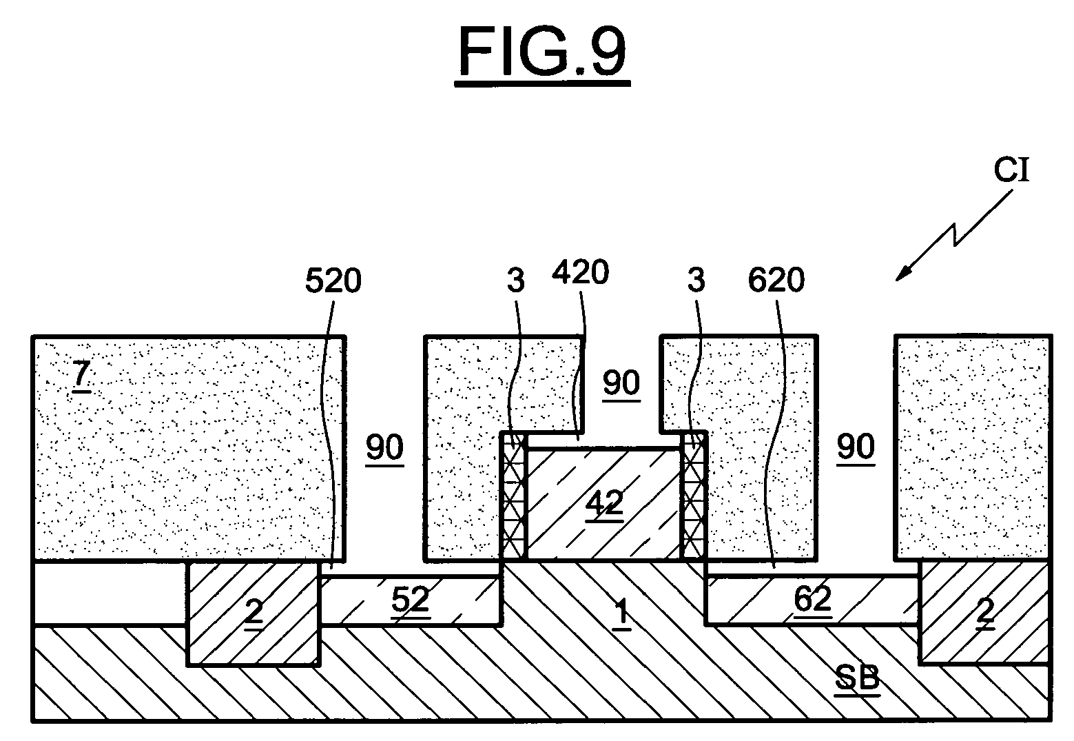
- the selectively removable material present in the zones 510, 610 and 410, is selectively removed (FIG. 9) to obtain cavities 520, 620 and 420 overlying the diffused source 52, drain regions. 62 and grid 42.
- the dimension of the cavities is greater than the opening of the orifice.
- This selective shrinkage can be carried out by any known method, for example by means of an oxidizing chemistry such as a 40 ml solution HNO 3 70% + 20 ml H 2 O 2 + 5 ml HF 0.5% or by plasma etching isotropic.
- an oxidizing chemistry such as a 40 ml solution HNO 3 70% + 20 ml H 2 O 2 + 5 ml HF 0.5% or by plasma etching isotropic.
- One or more electrically conductive materials are then deposited by known methods, which makes it possible to simultaneously fill the cavities obtained previously (FIG. 10) to obtain source regions 52, drain 62 and gate regions 42 surmounted by electrically conductive regions, for example metallizations, 53, 63 and 43, and vias of connections 91 which are also electrically conductive between these metallizations and the surface of the integrated circuit.
- metallization surfaces 43, 53, 63 are obtained greater than the opening of the vias, which makes it possible to reduce the contact resistance without increasing the lateral dimensions of the vias. which makes it possible to preserve the density of integration of the interconnections.
- the cavities 420, 520, 620 and the etching apertures 90 can be filled with tungsten (W) for example by a chemical vapor deposition (CVD) known per se, for example in a temperature range of 500 ° C to 600 ° C, or by a deposit of the type ALD (Atomic Layer Deposition) also known per se, for example in a temperature range of 200 ° C to 300 ° C.
- CVD chemical vapor deposition
- ALD Atomic Layer Deposition
- Copper (Cu), Cobalt (Co) or Nickel (Ni) can also be used using electrochemical deposition at room temperature. This being particularly the case with copper, it is preferable to first deposit a barrier layer, for example made of titanium nitride (TiN) using chemical vapor deposition, or tantalum (Ta).
- a barrier layer for example made of titanium nitride (TiN) using chemical vapor deposition, or tantalum (Ta).
- Tantalum nitride can also be used by using an ALD type deposit, for example in a temperature range of 200 ° C to 300 ° C.
- metal compound comprising aluminum (A1) and a small percentage, for example 5%, of silicon.
- metal oxides such as, for example, an indium oxide such as that known under the name ITO (Indium Thin Oxide).
- the excess metal for example, is removed for example by a chemical mechanical polishing and a metallization level M0 is produced, by known means, to obtain the integrated circuit of FIG. 11.
- FIG. 11 thus shows an integrated circuit IC comprising a transistor according to one embodiment of the invention.
- the integrated circuit comprises a substrate SB, in which active areas 1 have been made between the isolation zones 2 of the substrate.
- a transistor T has been made in and on the active area 1 of the substrate SB.
- the electrodes (source 52, drain 62 and gate 42) of the transistor are covered with electrically conductive contacts, for example all-metal contacts and formed of surface metallizations 53, 63 and 43 and metal vias 91 connected to the metallization level M0.
- FIG. 12 schematically illustrates a polysilicon line 75 forming a resistor, on which it has been realized, for example in accordance with the embodiment described above, an all-metal contact point.
- this resistive line of polysilicon 75 resting for example on an underlying insulating material 70, is provided locally with an all-metal contact point.
- This handshake comprises, as explained above, a metal surface area 750 and a metal inter-connection 91, formed in an upper insulating material 7.
- the via 91 makes it possible to electrically connect the metallization 750 of the resistor 75 to the upper metallization level M i of the integrated circuit.
- the metal surface area is obtained according to the embodiment above, for example from a Germanium implantation localized by a resin mask.
Landscapes
- Electrodes Of Semiconductors (AREA)
- Internal Circuitry In Semiconductor Integrated Circuit Devices (AREA)
- Insulated Gate Type Field-Effect Transistor (AREA)
Abstract

Description
- La présente invention concerne les circuits intégrés, notamment leur fabrication, et plus particulièrement la prise de contact sur une région du circuit intégré.
- Une prise de contact sur une région d'un circuit intégré, par exemple sur la région de source, de drain ou de grille d'un transistor, ou bien sur une ligne de polysilicium formant une résistance, consiste généralement actuellement en une siliciuration (c'est-à-dire une formation d'un siliciure de métal) de la partie supérieure de ladite région puis après avoir déposé un matériau isolant sur ladite région, par exemple du dioxyde de silicium, à ouvrir un orifice, communément appelé « via » par l'homme du métier, et à remplir le via d'un métal qui va venir au contact de la zone siliciurée. Ce via va ainsi permettre une connexion électrique entre la région semi-conductrice siliciurée et un niveau de métallisation du circuit intégré.
- Un tel procédé présente de nombreux inconvénients. Parmi ceux-ci, on peut citer par exemple la complexité et le coût de réalisation, mais également le problème de la résistance de la couche de siliciure ainsi que le problème de l'interface entre le siliciure de métal et le silicium. En effet, si cette interface n'est pas correcte, il peut en résulter un perçage des jonctions, une augmentation de la résistance, ou encore un décollement du siliciure de métal. L'interface entre zone siliciurée et le métal remplissant le via doit être parfaitement contrôlé. Aussi, est-il nécessaire alors de prévoir un nettoyage des fonds de contact après l'ouverture des vias, de façon à minimiser les risques d'obtenir une interface de mauvaise qualité. Et par conséquent, ceci augmente encore la complexité et le coût de réalisation.
- L'invention vise à remédier à ces inconvénients.
- Un but de l'invention est de proposer une réalisation d'une prise de contact qui soit radicalement différente de celle actuellement utilisée dans l'art antérieur.
- L'invention a pour but de proposer une réalisation d'une prise de contact qui soit extrêmement simple à effectuer avec un rendement très bon, en s'affranchissant notamment du nettoyage des fonds de contact effectué dans l'art antérieur.
- L'invention a encore pour but de proposer une prise de contact présentant une résistance très faible et en tout cas plus faible que celle obtenue dans l'art antérieur par siliciuration.
- L'invention a encore pour but de diminuer la résistance de contact associée et ce sans augmenter l'ouverture du via, afin de préserver la densité d'intégration des interconnexions.
- Selon un aspect de l'invention, il est proposé un procédé de réalisation d'au moins une prise de contact sur au moins une région d'un circuit intégré, dans lequel on modifie localement ladite région de façon à créer une zone s'étendant jusqu'à une partie au moins de la surface de ladite région, cette zone étant formée d'un matériau sélectivement éliminable par rapport au matériau de ladite région. On recouvre ladite région avec un matériau isolant et on forme dans le matériau isolant un orifice débouchant à la surface de ladite zone. On élimine le matériau sélectivement éliminable de ladite zone à travers ledit orifice de façon à former une cavité à la place de ladite zone. Et on remplit ladite cavité et ledit orifice avec au moins un matériau électriquement conducteur, par exemple métallique. On peut ainsi obtenir une prise de contact par exemple entièrement métallique sur ladite région.
- Selon cet aspect, l'invention prévoit ainsi en particulier la réalisation simultanée d'une métallisation sur la région semi-conductrice du circuit intégré, et du via d'interconnexion permettant de connecter cette métallisation à un niveau de métallisation supérieure du circuit intégré. Ceci est particulièrement simple à réaliser à moindre coût. Les rendements sont très bons car le choix des matériaux électriquement conducteurs et de la température est très vaste. A cet égard, on peut envisager, non limitativement, de remplir la cavité et l'orifice de gravure avec un seul et même métal, mais aussi avec plusieurs métaux ou composés métalliques différents, ou encore avec un ou plusieurs oxydes métalliques, comme par exemple un oxyde d'indium tel que celui connu de l'homme du métier sous la dénomination anglosaxonne ITO (Indium Thin Oxide).
- Par ailleurs, le problème du nettoyage des fonds de contact après l'ouverture des vias ne se pose pas ici car selon un mode de mise en oeuvre de l'invention, on prévoit l'élimination d'une couche de matériau sélectivement éliminable et, de ce fait, l'interface ainsi obtenue est quasi parfaite.
- Par ailleurs, la couche métallisée située en surface de la région sur laquelle on prend le contact, peut présenter une résistance très faible, et en tout cas plus faible que celle d'un siliciure de métal.
- Par ailleurs l'épaisseur de cette couche métallisée est parfaitement déterminable et peut être aisément ajustée en fonction de l'application envisagée.
- En outre, la métallisation se fait à un instant tardif dans le procédé de réalisation des composants sur lesquels il est nécessaire de prendre un contact métallique. De ce fait, le bilan thermique est plus faible. Les jonctions peuvent être réalisées en surface sur une très faible profondeur parce que le bilan thermique est faible et parce que la métallisation de la jonction peut être effectuée sur une très faible épaisseur.
- Par ailleurs, selon un mode de mise en oeuvre particulièrement avantageux de l'invention, l'ouverture de la cavité est plus grande que celle dudit orifice, ce qui permet d'augmenter la surface du contact électriquement conducteur (c'est-à-dire la zone remplie du matériau électriquement conducteur) et par conséquent de diminuer la résistance de contact et ce sans augmenter les dimensions du via, c'est-à-dire celles de l'orifice. On préserve donc la densité d'intégration des interconnexions. Et ceci est rendu possible car la définition de l'emplacement et des dimensions de la cavité est effectuée avant la gravure de l'orifice et que la formation effective de la cavité est effectuée après ladite gravure et à travers l'orifice gravé.
- L'invention s'applique en particulier pour des prises de contact sur des régions de composants actifs, tels que des transistors, ou bien passifs, tels que des résistances, par exemple des lignes résistives en polysilicium. L'invention permet ainsi en particulier de diminuer les résistances d'accès à toutes sortes de dispositifs, en particulier les transistors bipolaires.
- L'invention peut également s'appliquer à tout élément, passif ou actif d'un circuit intégré sur lequel il est nécessaire de prendre un contact.
- L'épaisseur de la zone résultant de la modification locale de ladite région peut avoir une épaisseur quelconque, que l'homme du métier saura choisir en fonction de l'application envisagée. Cela étant, il est particulièrement avantageux que la zone soit une zone surfacique très fine, ce qui est aisément rendu possible par un mode de mise en oeuvre du procédé selon l'invention. A cet égard, l'épaisseur de ladite zone surfacique est par exemple inférieure à 50 nm
- Le matériau de ladite région sur laquelle on souhaite prendre le contact, est par exemple un matériau à base de silicium, par exemple du silicium mono cristallin ou poly cristallin. Dans ce cas, le matériau sélectivement éliminable peut être un alliage de silicium et de germanium.
- On forme par exemple ladite zone par implantation de dopants, par exemple par implantation de germanium, cette implantation pouvant être par exemple localisée par un masquage de resine ou bien auto-alignée sur un motif préexistant d'un circuit intégré. Il serait égament possible dans certains cas d'implanter de l'oxygène ou de l'azote.
- On peut former ledit orifice dans le matériau isolant par une gravure chimique ou plasma.
- Selon un mode de mise en oeuvre, on élimine le matériau de ladite zone par une gravure sélective.
- Dans certains cas, toute la surface de la région peut être métallisée. En d'autres termes, selon un tel mode de mise en oeuvre, ladite zone s'étend jusqu'à la totalité de ladite région.
- Ladite région peut être une région de source, de drain, ou de grille d'un transistor à effet de champ, ou une région d'émetteur, de collecteur ou de base d'un transistor bipolaire.
- Lorsque l'invention s'applique à la fabrication d'un transistor MOS, cette fabrication comprend, selon un mode de mise en oeuvre :
- a) la formation des régions de grille, source et drain du transistor, et,
- b) la réalisation simultanée des prises de contact métalliques respectives sur les régions de source et de drain telles que définies ci avant. Le matériau isolant dans lequel on forme lesdits orifices débouchant sur les régions de source et de drain recouvre alors la structure obtenue à l'étape a).
- Ainsi, il est possible d'obtenir selon un mode de mise en oeuvre de l'invention des métallisations auto alignées sur les régions de source et drain du transistor MOS et ce sans problème de court-circuit des jonctions sous-jacentes.
- On peut également réaliser simultanément la métallisation et la prise de contact métallique sur la région de grille.
- Ainsi, dans le cas d'un transistor MOS, par exemple, l'invention est remarquable en ce sens que l'on réalise simultanément et de façon auto alignée les métallisations de source de drain et de grille ainsi que les vias interconnectant ces métallisations au niveau de métallisation supérieure du circuit intégré.
- Selon un autre aspect de l'invention il est proposé également un circuit intégré comprenant au moins une région équipée d'une prise de contact entièrement métallique obtenue par le procédé tel que défini ci avant.
- Cette région peut faire partie d'un composant passif ou actif.
- Ce composant peut être ainsi une résistance formée d'une ligne de polysilicium ou bien un transistor obtenu par un procédé de fabrication tel que défini ci avant.
- D'autres avantages et caractéristiques de l'invention apparaîtront à l'examen de la description détaillée de modes de réalisation et de mise en oeuvre, nullement limitatifs, et des dessins annexés, sur lesquels :
- les figures 1 à 10 illustrent schématiquement les principales étapes d'un mode de mise en oeuvre du procédé selon la présente invention, et la figure 11 représente schématiquement un transistor obtenu par un tel mode de mise en oeuvre, au sein d'un circuit intégré,et
- la figure 12 illustre schématiquement un autre composant d'un circuit intégré équipé d'une prise de contact selon un mode de réalisation de l'invention.
- On va maintenant décrire plus en détails, les principales étapes d'un mode de mise en oeuvre du procédé selon l'invention.
- Sur la figure 1, on forme sur un substrat SB, par exemple en silicium, une zone active 1 entre deux zones d'isolation 2, lesdites zones d'isolation pouvant être des tranchées d'isolation. Ces tranchées d'isolation peuvent être, par exemple, profondes de type DTI (« Deep Trench Isolation ») ou peu profondes de type STI (« Shallow Trench Isolation »).
- Sur la zone active 1, on réalise une région de grille initiale 4, pouvant également être en polysilicium, par des moyens connus en soi.
- On procède ensuite à la matérialisation des régions de source et de drain (figure 2). Cette matérialisation est effectuée, par exemple, en procédant à deux implantations 40 de dopants respectivement effectuées avant et après la formation d'espaceurs 3 entourant la grille. La nature des dopants est choisie en fonction du type N ou P du transistor sur le circuit CI. La grille initiale 4 servant de masque pour les implantations ioniques, on obtient des régions de source et de drain auto-alignées avec la région de grille initiale 4 et avec la zone active 1 délimitée par les régions d'isolations 2.
- On procède également à une implantation de dopants dans la grille.
- Ces diverses implantations permettent de matérialiser, comme illustré sur la Figure 3, des régions diffusées de source 51, de drain 61, et de grille 41. On notera également bien entendu que la grille du transistor est dans cet exemple une grille isolée, séparée du substrat 1 par un oxyde de grille, non représenté ici à des fins de simplification.
- On procède ensuite (Figure 4) à une implantation 400 de germanium par exemple, sur le circuit intégré CI. Cette implantation est donc effectuée « pleine plaque » (« full sheet »).
- Comme illustré sur la Figure 5, cette implantation 400 a une énergie choisie de façon à former des zones superficielles 410, 510 et 610 et ce, respectivement dans les régions 41, 51 et 61. Ces zones surfaciques 410, 510 et 610 sont alors formées d'un matériau sélectivement éliminable par rapport au silicium formant les régions 41, 51 et 61. Plus précisément, dans le cas présent, ces zones 410, 510 et 610 sont formées d'un alliage de silicium germanium SiGe.
- Un recuit peut en outre être effectué de façon à recristalliser les matériaux et ainsi à mieux définir les frontières entre le matériau formant les régions 51, 61 et 41 et le matériau sélectivement éliminable dans les zones de source 510, 610 et 410. Ce recuit peut par exemple être effectué à une température de 800 à 900 °C.
- La surface du circuit est ensuite recouverte par des moyens connus, d'une couche d'un matériau isolant 7, ladite couche 7 étant constituée par exemple de dioxyde de silicium (Figure 6). Cette couche 7 est surmontée d'une couche de résine 8 (Figure 7), également obtenue par des moyens connus, dans laquelle on forme de façon connue des orifices 9 matérialisant l'emplacement 9 des futurs vias de connexions.
- Puis on procède, à travers les orifices 9 du masque de résine, à une gravure anisotrope du matériau isolant 7 de façon à obtenir des orifices de gravure 90 s'étendant jusqu'aux zones de source 510, de drain 610 et de grille 410 (Figure 8).
- C'est à travers les orifices 90 que le matériau sélectivement éliminable, présent dans les zones 510, 610 et 410, est retiré sélectivement (Figure 9) pour obtenir des cavités 520, 620 et 420 surmontant les régions diffusées de source 52, de drain 62 et de grille 42.
- On notera ici que la dimension des cavités est supérieure à l'ouverture de l'orifice.
- Ce retrait sélectif peut se faire par tout procédé connu, par exemple au moyen d'une chimie oxydante telle qu'une solution 40 ml HNO3 70 % + 20 ml H2O2 + 5 ml HF 0,5 % ou par attaque plasma isotrope.
- On procède ensuite au dépôt d'un ou de plusieurs matériaux électriquement conducteurs par des méthodes connues, ce qui permet de remplir simultanément les cavités obtenues précédemment (Figure 10) pour obtenir des régions de source 52, de drain 62, de grille 42 surmontées par des zones électriquement conductrices, par exemple des métallisations, 53, 63 et 43, et des vias de connexions 91 également électriquement conducteurs entre ces métallisations et la surface du circuit intégré.
- Puisque l'ouverture des cavités est supérieure à celle des orifices, on obtient des surfaces de métallisation 43, 53, 63 supérieures à l'ouverture des vias, ce qui permet de diminuer la résistance de contact sans augmenter les dimensions latérales des vias, ce qui permet de préserver la densité d'intégration des interconnexions.
- A cet égard on peut remplir les cavités 420, 520, 620 et les orifices de gravure 90 par du tungstène (W) par exemple par un dépôt chimique en phase vapeur (dépôt CVD) connu en soi, par exemple dans une fourchette de températures de 500°C à 600°C , ou bien par un dépôt du type ALD (Atomic Layer Deposition) également connu en soi, par exemple dans une fourchette de températures de 200°C à 300°C.
- On peut également utiliser du cuivre (Cu), du Cobalt (Co) ou du Nickel (Ni) en utilisant un dépôt électrochimique à température ambiante. Cela étant notamment dans le cas du cuivre il est préférable de déposer préalablement une couche barrière par exemple en nitrure de titane (TiN) en utilisant un dépôt chimique en phase vapeur, ou en tantale (Ta).
- On peut aussi utiliser du nitrure de tantale (TaN) en utilisant un dépôt du type ALD, par exemple dans une fourchette de températures de 200°C à 300°C.
- On peut aussi utiliser du polysilicium fortement dopé en utilisant un dépôt LPCVD (dépôt CVD à basse pression) dans un four par exemple entre 700°C et 800°C, ou bien un dépôt du type ALD par exemple dans une fourchette de températures de 200°C à 300°C
- On peut encore utiliser un composé métallique comportant de l'aluminium (A1) et un faible pourcentage, par exemple 5%, de silicium.
- On peut encore utiliser des oxydes métalliques, comme par exemple un oxyde d'indium tel que celui connu sous la dénomination ITO (Indium Thin Oxyde).
- L'excès de métal, par exemple, est éliminé par exemple par un polissage mécano-chimique et un niveau de métallisation M0 est réalisé, par des moyens connus, pour obtenir le circuit intégré de la figure 11.
- Sur la figure 11, on a donc représenté un circuit intégré CI comprenant un transistor selon un mode de réalisation de l'invention.
- Le circuit intégré comporte un substrat SB, dans lequel des zones actives 1 ont été réalisées entre les zones d'isolations 2 du substrat. Un transistor T a été réalisé dans et sur la zone active 1 du substrat SB. Les électrodes (source 52, drain 62 et grille 42) du transistor sont recouvertes de prises de contact électriquement conductrices, par exemple entièrement métalliques et formées de métallisations surfaciques 53, 63 et 43 et de vias métalliques 91 connectés au niveau de métallisation M0.
- L'invention n'est pas limitée à la réalisation de prises de contact auto alignées sur un transistor mais s'applique à tout composant passif ou actif d'un circuit intégré sur lequel il est nécessaire de prendre une prise de contact auto-alignée ou non. A titre indicatif, la figure 12 illustre schématiquement une ligne de polysilicium 75, formant une résistance, sur laquelle on a réalisé, par exemple conformément au mode de mise en oeuvre décrit ci-avant, une prise de contact entièrement métallique.
- Plus précisément, cette ligne résistive de polysilicium 75, reposant par exemple sur un matériau isolant sous-jacent 70, est pourvue localement d'une prise de contact entièrement métallique. Cette prise de contact comporte comme expliqué ci avant, une zone surfacique métallique 750 et un via métallique d'inter connexion 91, ménagé au sein d'un matériau isolant supérieur 7. Le via 91 permet de relier électriquement la métallisation 750 de la résistance 75 au niveau de métallisation supérieure Mi du circuit intégré. La zone surfacique métallique est obtenue selon le mode de mise en oeuvre ci avant par exemple à partir d'une implantation de Germanium localisée par un masque en résine.
Claims (17)
- Procédé de réalisation d'au moins une prise de contact sur au moins une région d'un circuit intégré, caractérisé par le fait qu'on modifie localement ladite région (51) de façon à créer une zone (510) s'étendant jusqu'à une partie au moins de la surface de ladite région et formée d'un matériau sélectivement éliminable par rapport au matériau de ladite région, on recouvre ladite région avec un matériau isolant (7), on forme dans le matériau isolant un orifice (90) débouchant à la surface de ladite zone, on élimine le matériau sélectivement éliminable de ladite zone à travers ledit orifice de façon à former une cavité (520) à la place de ladite zone, et on remplit ladite cavité et ledit orifice avec au moins un matériau électriquement conducteur (91).
- Procédé selon la revendication 1, dans lequel l'ouverture de la cavité (250) est plus grande que l'ouverture de l'orifice (90).
- Procédé selon la revendication 1 ou 2, dans lequel ladite zone (510) est une zone surfacique dont l'épaisseur est inférieure à 50 nm.
- Procédé selon l'une des revendications précédentes, dans lequel le matériau de ladite région est un matériau à base de silicium, par exemple du silicium monocristallin ou polycristallin, et dans lequel le matériau sélectivement éliminable est un alliage de silicium et de germanium.
- Procédé selon l'une des revendications précédentes, caractérisé par le fait qu'on forme ladite zone (510) par implantation de dopants, par exemple par implantation de germanium.
- Procédé selon la revendication 5, dans lequel on forme ladite zone (510, 750) par une implantation de Germanium effectuée de manière localisée ou pleine plaque.
- Procédé selon l'une des revendications précédentes, dans lequel on forme ledit orifice (90) par une gravure chimique ou plasma.
- Procédé selon l'une des revendications précédentes, dans lequel on élimine le matériau de ladite zone (510) par une gravure sélective.
- Procédé selon l'une des revendications précédentes, dans lequel ladite zone s'étend jusqu'à la totalité de la surface de ladite région.
- Procédé selon l'une des revendications précédentes, dans lequel ladite région appartient à un composant électronique passif ou actif du circuit intégré.
- Procédé selon l'une des revendications précédentes, dans lequel ladite région est une région de source, de drain ou de grille d'un transistor à effet de champ, ou une région d'émetteur, de collecteur ou de base d'un transistor bipolaire
- Procédé de fabrication d'un transistor MOS, caractérisé par le fait qu'il comprend a) la formation des régions de grille, source et drain du transistor, et, b) la réalisation simultanée des prises de contact respectives sur les régions de source et de drain selon l'une des revendications 1 à 11, le matériau isolant dans lequel on forme lesdits orifices débouchant sur les régions de source et de drain, recouvrant la structure obtenue à l'étape a) .
- Procédé selon la revendication 12, dans lequel on réalise également simultanément la prise de contact sur la région de grille.
- Circuit intégré comprenant au moins une région équipée d'une prise de contact obtenue par le procédé selon l'une des revendications 1 à 13.
- Circuit intégré selon la revendication 14, dans lequel ladite région fait partie d'un composant passif ou actif.
- Circuit intégré selon la revendication 15, dans lequel le composant est une résistance formée d'une ligne de polysilicium.
- Circuit intégré selon la revendication 15, dans lequel le composant est un transistor obtenu par le procédé selon la revendication 12 ou 13.
Applications Claiming Priority (1)
| Application Number | Priority Date | Filing Date | Title |
|---|---|---|---|
| FR0411123 | 2004-10-20 |
Publications (2)
| Publication Number | Publication Date |
|---|---|
| EP1650796A2 true EP1650796A2 (fr) | 2006-04-26 |
| EP1650796A3 EP1650796A3 (fr) | 2010-12-08 |
Family
ID=34950912
Family Applications (1)
| Application Number | Title | Priority Date | Filing Date |
|---|---|---|---|
| EP05292061A Withdrawn EP1650796A3 (fr) | 2004-10-20 | 2005-10-04 | Procédé de prise de contact sur une région d'un circuit intégré, en particulier sur les électrodes d'un transistor |
Country Status (4)
| Country | Link |
|---|---|
| US (2) | US7601634B2 (fr) |
| EP (1) | EP1650796A3 (fr) |
| JP (1) | JP2006121082A (fr) |
| CN (1) | CN100477156C (fr) |
Cited By (2)
| Publication number | Priority date | Publication date | Assignee | Title |
|---|---|---|---|---|
| WO2006134553A3 (fr) * | 2005-06-16 | 2008-06-19 | Nxp Bv | Dispositif a semi-conducteur comprenant une electrode de polysilicium |
| US8021986B2 (en) | 2009-06-25 | 2011-09-20 | Commissariat à l'énergie atomique et aux energies alternatives | Method for producing a transistor with metallic source and drain |
Families Citing this family (4)
| Publication number | Priority date | Publication date | Assignee | Title |
|---|---|---|---|---|
| US7670896B2 (en) * | 2006-11-16 | 2010-03-02 | International Business Machines Corporation | Method and structure for reducing floating body effects in MOSFET devices |
| US10381448B2 (en) * | 2016-05-26 | 2019-08-13 | Tokyo Electron Limited | Wrap-around contact integration scheme |
| US9876030B1 (en) * | 2016-08-24 | 2018-01-23 | Toshiba Memory Corporation | Semiconductor device and method for manufacturing same |
| KR20220158145A (ko) * | 2021-05-20 | 2022-11-30 | 삼성전자주식회사 | 이미지 센서 및 이의 제조 방법 |
Family Cites Families (18)
| Publication number | Priority date | Publication date | Assignee | Title |
|---|---|---|---|---|
| JPS58106846A (ja) * | 1981-12-18 | 1983-06-25 | Nec Corp | 半導体装置の製造方法 |
| JPH05291506A (ja) * | 1992-04-13 | 1993-11-05 | Toshiba Corp | 半導体集積回路装置及びその製造方法 |
| JPH08130195A (ja) * | 1994-11-01 | 1996-05-21 | Mitsubishi Electric Corp | 半導体装置及びその製造方法 |
| JP3384158B2 (ja) * | 1994-12-28 | 2003-03-10 | ヤマハ株式会社 | 半導体装置の製造方法 |
| JP2701803B2 (ja) * | 1995-08-28 | 1998-01-21 | 日本電気株式会社 | 半導体装置の製造方法 |
| JP3961044B2 (ja) * | 1996-05-14 | 2007-08-15 | シャープ株式会社 | 電子回路装置 |
| JP2959514B2 (ja) * | 1997-03-26 | 1999-10-06 | 日本電気株式会社 | 半導体装置及び半導体装置の製造方法 |
| US6281131B1 (en) * | 1998-02-27 | 2001-08-28 | Micron Technology, Inc. | Methods of forming electrical contacts |
| JP2000286397A (ja) * | 1999-03-30 | 2000-10-13 | Nec Corp | 半導体装置の製造方法 |
| JP2001127151A (ja) * | 1999-10-26 | 2001-05-11 | Fujitsu Ltd | 半導体装置およびその製造方法 |
| WO2003009353A1 (fr) * | 2001-07-18 | 2003-01-30 | Infineon Technologies Ag | Procede selectif de gravure de base |
| KR100434697B1 (ko) * | 2001-09-05 | 2004-06-07 | 주식회사 하이닉스반도체 | 반도체소자의 제조방법 |
| KR20040017037A (ko) * | 2002-08-20 | 2004-02-26 | 삼성전자주식회사 | 반도체 콘택 구조 및 그 형성 방법 |
| KR100953332B1 (ko) * | 2002-12-31 | 2010-04-20 | 동부일렉트로닉스 주식회사 | 반도체 장치의 제조 방법 |
| EP1503411A1 (fr) * | 2003-07-30 | 2005-02-02 | St Microelectronics S.A. | Lignes conductrices enterrées dans des zones d'isolement |
| US7084025B2 (en) * | 2004-07-07 | 2006-08-01 | Chartered Semiconductor Manufacturing Ltd | Selective oxide trimming to improve metal T-gate transistor |
| US7135724B2 (en) * | 2004-09-29 | 2006-11-14 | International Business Machines Corporation | Structure and method for making strained channel field effect transistor using sacrificial spacer |
| US7074713B2 (en) * | 2004-09-30 | 2006-07-11 | Freescale Semiconductor, Inc. | Plasma enhanced nitride layer |
-
2005
- 2005-10-04 EP EP05292061A patent/EP1650796A3/fr not_active Withdrawn
- 2005-10-14 US US11/250,641 patent/US7601634B2/en active Active
- 2005-10-18 CN CNB2005101161054A patent/CN100477156C/zh not_active Expired - Fee Related
- 2005-10-18 JP JP2005302800A patent/JP2006121082A/ja active Pending
-
2009
- 2009-08-10 US US12/538,723 patent/US8299541B2/en not_active Expired - Fee Related
Cited By (3)
| Publication number | Priority date | Publication date | Assignee | Title |
|---|---|---|---|---|
| WO2006134553A3 (fr) * | 2005-06-16 | 2008-06-19 | Nxp Bv | Dispositif a semi-conducteur comprenant une electrode de polysilicium |
| US7790545B2 (en) | 2005-06-16 | 2010-09-07 | Nxp B.V. | Semiconductor device having a polysilicon electrode including amorphizing, recrystallising, and removing part of the polysilicon electrode |
| US8021986B2 (en) | 2009-06-25 | 2011-09-20 | Commissariat à l'énergie atomique et aux energies alternatives | Method for producing a transistor with metallic source and drain |
Also Published As
| Publication number | Publication date |
|---|---|
| EP1650796A3 (fr) | 2010-12-08 |
| CN1783456A (zh) | 2006-06-07 |
| US20100025773A1 (en) | 2010-02-04 |
| CN100477156C (zh) | 2009-04-08 |
| JP2006121082A (ja) | 2006-05-11 |
| US20060091477A1 (en) | 2006-05-04 |
| US7601634B2 (en) | 2009-10-13 |
| US8299541B2 (en) | 2012-10-30 |
Similar Documents
| Publication | Publication Date | Title |
|---|---|---|
| KR102526836B1 (ko) | 코발트계 인터커넥트 및 그의 제조 방법 | |
| EP0420748B1 (fr) | Procédé de fabrication d'un circuit intégré MIS haute tension | |
| KR101366201B1 (ko) | 콘택 영역들에 금속 규화물 영역을 국부적으로 구비한 트랜지스터 및 그 트랜지스터를 제조하는 방법 | |
| US8030210B2 (en) | Contact barrier structure and manufacturing methods | |
| US8120119B2 (en) | Stressed barrier plug slot contact structure for transistor performance enhancement | |
| US7719062B2 (en) | Tuned tensile stress low resistivity slot contact structure for n-type transistor performance enhancement | |
| TW200525750A (en) | FET gate structure with metal gate electrode and silicide contact | |
| US7790611B2 (en) | Method for FEOL and BEOL wiring | |
| EP1406307A1 (fr) | Circuit intégré à couche enterrée fortement conductrice | |
| US8299541B2 (en) | Process for producing a contact pad on a region of an integrated circuit, in particular on the electrodes of a transistor | |
| KR100945791B1 (ko) | 상변화 메모리 소자 및 그 제조 방법 | |
| EP0414618B1 (fr) | Transistor MOS en couche mince avec la zone de canal reliée à la source et son procédé de fabrication | |
| US11784090B2 (en) | Semiconductor structure | |
| KR19980070785A (ko) | 반도체 장치 및 그 제조 방법 | |
| EP0522938B1 (fr) | Procédé de fabrication d'un transistor à effet de champ vertical, et transistor obtenu par ce procédé | |
| FR2750534A1 (fr) | Transistor et procede de realisation d'un transistor a contacts et a isolation de champ auto-alignes | |
| FR2864345A1 (fr) | Realisation de la peripherie d'une diode schottky a tranchees mos | |
| EP1223614B1 (fr) | Procédé de fabrication d'un substrat monocristallin, et circuit intégré comportant un tel substrat | |
| FR2947384A1 (fr) | Procede de realisation d'un transistor a source et drain metalliques | |
| EP3136429B1 (fr) | Formation de contacts ohmiques pour un dispositif dote d'une region en materiau iii-v et d'une region en un autre materiau semi-conducteur | |
| KR20000043055A (ko) | 반도체 소자의 비트 라인 형성 방법 | |
| FR2828766A1 (fr) | Circuit integre comprenant des elements actifs et au moins un element passif, notamment des cellules memoire dram et procede de fabrication | |
| KR100641910B1 (ko) | 반도체 소자의 금속배선 형성방법 | |
| FR2804793A1 (fr) | Procede d'ajustement de la valeur de resistance de grille d'un transistor d'un circuit integre et circuit integre correspondant | |
| JP2007250624A (ja) | 半導体装置の製造方法 |
Legal Events
| Date | Code | Title | Description |
|---|---|---|---|
| PUAI | Public reference made under article 153(3) epc to a published international application that has entered the european phase |
Free format text: ORIGINAL CODE: 0009012 |
|
| AK | Designated contracting states |
Kind code of ref document: A2 Designated state(s): AT BE BG CH CY CZ DE DK EE ES FI FR GB GR HU IE IS IT LI LT LU LV MC NL PL PT RO SE SI SK TR |
|
| AX | Request for extension of the european patent |
Extension state: AL BA HR MK YU |
|
| RIN1 | Information on inventor provided before grant (corrected) |
Inventor name: CERUTTI, ROBIN Inventor name: CORONEL, PHILIPPE Inventor name: LENOBLE, DAMIEN |
|
| RIN1 | Information on inventor provided before grant (corrected) |
Inventor name: CERUTTI, ROBIN Inventor name: CORONEL, PHILIPPE Inventor name: LENOBLE, DAMIEN |
|
| PUAL | Search report despatched |
Free format text: ORIGINAL CODE: 0009013 |
|
| AK | Designated contracting states |
Kind code of ref document: A3 Designated state(s): AT BE BG CH CY CZ DE DK EE ES FI FR GB GR HU IE IS IT LI LT LU LV MC NL PL PT RO SE SI SK TR |
|
| AX | Request for extension of the european patent |
Extension state: AL BA HR MK YU |
|
| RIC1 | Information provided on ipc code assigned before grant |
Ipc: H01L 21/768 20060101AFI20060207BHEP |
|
| AKY | No designation fees paid | ||
| REG | Reference to a national code |
Ref country code: DE Ref legal event code: R108 |
|
| REG | Reference to a national code |
Ref country code: DE Ref legal event code: R108 Effective date: 20110822 |
|
| STAA | Information on the status of an ep patent application or granted ep patent |
Free format text: STATUS: THE APPLICATION IS DEEMED TO BE WITHDRAWN |
|
| 18D | Application deemed to be withdrawn |
Effective date: 20110609 |