EP1643261A1 - Nuclear magnetic resonance apparatus - Google Patents
Nuclear magnetic resonance apparatus Download PDFInfo
- Publication number
- EP1643261A1 EP1643261A1 EP05016795A EP05016795A EP1643261A1 EP 1643261 A1 EP1643261 A1 EP 1643261A1 EP 05016795 A EP05016795 A EP 05016795A EP 05016795 A EP05016795 A EP 05016795A EP 1643261 A1 EP1643261 A1 EP 1643261A1
- Authority
- EP
- European Patent Office
- Prior art keywords
- substrates
- probe
- spacer
- coils
- coil
- Prior art date
- Legal status (The legal status is an assumption and is not a legal conclusion. Google has not performed a legal analysis and makes no representation as to the accuracy of the status listed.)
- Withdrawn
Links
Images


Classifications
-
- G—PHYSICS
- G01—MEASURING; TESTING
- G01R—MEASURING ELECTRIC VARIABLES; MEASURING MAGNETIC VARIABLES
- G01R33/00—Arrangements or instruments for measuring magnetic variables
- G01R33/20—Arrangements or instruments for measuring magnetic variables involving magnetic resonance
- G01R33/28—Details of apparatus provided for in groups G01R33/44 - G01R33/64
- G01R33/32—Excitation or detection systems, e.g. using radio frequency signals
- G01R33/34—Constructional details, e.g. resonators, specially adapted to MR
- G01R33/34046—Volume type coils, e.g. bird-cage coils; Quadrature bird-cage coils; Circularly polarised coils
- G01R33/34053—Solenoid coils; Toroidal coils
-
- G—PHYSICS
- G01—MEASURING; TESTING
- G01R—MEASURING ELECTRIC VARIABLES; MEASURING MAGNETIC VARIABLES
- G01R33/00—Arrangements or instruments for measuring magnetic variables
- G01R33/20—Arrangements or instruments for measuring magnetic variables involving magnetic resonance
- G01R33/28—Details of apparatus provided for in groups G01R33/44 - G01R33/64
- G01R33/32—Excitation or detection systems, e.g. using radio frequency signals
- G01R33/34—Constructional details, e.g. resonators, specially adapted to MR
- G01R33/34046—Volume type coils, e.g. bird-cage coils; Quadrature bird-cage coils; Circularly polarised coils
- G01R33/34069—Saddle coils
-
- G—PHYSICS
- G01—MEASURING; TESTING
- G01R—MEASURING ELECTRIC VARIABLES; MEASURING MAGNETIC VARIABLES
- G01R33/00—Arrangements or instruments for measuring magnetic variables
- G01R33/20—Arrangements or instruments for measuring magnetic variables involving magnetic resonance
- G01R33/28—Details of apparatus provided for in groups G01R33/44 - G01R33/64
- G01R33/32—Excitation or detection systems, e.g. using radio frequency signals
- G01R33/34—Constructional details, e.g. resonators, specially adapted to MR
- G01R33/34007—Manufacture of RF coils, e.g. using printed circuit board technology; additional hardware for providing mechanical support to the RF coil assembly or to part thereof, e.g. a support for moving the coil assembly relative to the remainder of the MR system
-
- G—PHYSICS
- G01—MEASURING; TESTING
- G01R—MEASURING ELECTRIC VARIABLES; MEASURING MAGNETIC VARIABLES
- G01R33/00—Arrangements or instruments for measuring magnetic variables
- G01R33/20—Arrangements or instruments for measuring magnetic variables involving magnetic resonance
- G01R33/28—Details of apparatus provided for in groups G01R33/44 - G01R33/64
- G01R33/32—Excitation or detection systems, e.g. using radio frequency signals
- G01R33/34—Constructional details, e.g. resonators, specially adapted to MR
- G01R33/34015—Temperature-controlled RF coils
- G01R33/34023—Superconducting RF coils
-
- G—PHYSICS
- G01—MEASURING; TESTING
- G01R—MEASURING ELECTRIC VARIABLES; MEASURING MAGNETIC VARIABLES
- G01R33/00—Arrangements or instruments for measuring magnetic variables
- G01R33/20—Arrangements or instruments for measuring magnetic variables involving magnetic resonance
- G01R33/28—Details of apparatus provided for in groups G01R33/44 - G01R33/64
- G01R33/32—Excitation or detection systems, e.g. using radio frequency signals
- G01R33/34—Constructional details, e.g. resonators, specially adapted to MR
- G01R33/34092—RF coils specially adapted for NMR spectrometers
Definitions
- the present invention relates to a nuclear magnetic resonance apparatus (hereafter, represented as "NMR apparatus"), and more particularly to an NMR apparatus characterized in the shape of a probe coil for transmitting a high-frequency signal to a sample placed in a predetermined uniform magnetic field (B 0 ) with a predetermined resonance frequency and/or receiving a free induction decay (FID) signal and its construction for mounting.
- NMR apparatus nuclear magnetic resonance apparatus
- B 0 uniform magnetic field
- FID free induction decay
- Nuclear magnetic resonance (NMR) measurement can be implemented by measuring response signals from atomic spins that constitute substances.
- the NMR measurement is an ultimate measuring technique that makes it possible to obtain microscopic information about substances.
- the basic principle behind the NMR measurement is as follows: a high-frequency magnetic field is applied to a sample placed in a uniform magnetic field. The response signals from spins thereby excited are received and analyzed. As a result, the properties of various substances can be measured. Conventionally, the NMR measurement has been used for studying solid state properties.
- the uniformity of magnetic field is one of the critical factors.
- a uniformity of 10 -9 or below is required in a space in which a sample as a measuring object exists.
- response signals (free induction decay signals, FID signals) from a sample are extremely weak.
- FID signals free induction decay signals
- a high-sensitivity reception system is required.
- the enhancement of the sensitivity of probe coils (antenna elements) that receive signals is a technical challenge the solving of which is indispensable to NMR measuring apparatuses.
- Application of a probe coil using a superconducting material whose resistance to high-frequency currents is extremely low is effective in solving this challenge.
- Superconducting materials are lower in resistance to high-frequency currents by two orders of magnitude or more than ordinary normal-conducting materials (e.g. metallic materials such as copper and gold). Therefore, resistive loss in a reception coil can be remarkably reduced, and the enhancement of sensitivity is accomplished.
- a probe coil formed of superconductor must be placed in a low-temperature environment.
- the apparatuses must be provided with a cooling mechanism. If this cooling mechanism is used to cool a semiconductor amplifier connected to the stage subsequent to the probe coil, the sensitivity of the entire reception system can be further enhanced.
- an NMR measuring apparatus characterized in its high resolution and high sensitivity: ensuring a uniform magnetic field in a sample space, and adopting a probe coil formed of superconductingmaterial.
- An NMR measuring apparatus provided with a cooling mechanism and a superconducting probe coil is described in Patent Document 1.
- Application of a superconducting coil is described in Patent Document 2 and Patent Document 3.
- superconducting solenoid coils are set (installed) to ensure the above-mentioned uniformity of high magnetic field.
- bird cage or saddle is adopted for the shape of a probe coil. This is for the purpose of suppressing the uniformity of magnetic field from being disturbed by the perfect diamagnetism of superconductor.
- a saddle or bird cage probe coil is formed of superconductor, especially, high-temperature superconductor to reduce the noise in the probe coil, the following problem arises: a superconducting film formed on a flat oxide single crystal substrate is utilized; therefore, the shape cannot be freely selected, and it is difficult to efficiently cover a sample. Though the noise in the coil caused by resistance can be reduced, as a result, the following problem arises: reduction in the filling factor related to shape lowers the efficiency of application of high-frequency signals.
- solenoid probe coil Adoption of solenoid probe coil is a promising measure to further enhance the sensitivity of NMR measurement. Solenoid probe coils make it possible to further enhance the filling factor than conventional bird cage-shaped coils. As a result, the enhancement of sensitivity can be accomplished.
- a solenoid probe coil must be installed so that the direction of its central axis is orthogonal to a static magnetic field. Therefore, if a solenoid probe coil is inserted into a conventionally used integral-type superconducting solenoid coil that generates a uniform magnetic field, a space in which a measurement sample is to be placed cannot be ensured. Consequently, to use a solenoid probe coil, such a constitution that a uniform superconducting magnet that generates a magnetic field is split must be adopted.
- An object of the present invention is to provide an NMR apparatus wherein the enhancement of the sensitivity of a probe coil that receives free induction decay (FID) signals in nuclear magnetic resonance (NMR) spectroscopy is accomplished.
- FID free induction decay
- NMR nuclear magnetic resonance
- Two methods can be used to provide a probe coil between two superconducting solenoid coils.
- One is a method in which it is inserted in the same direction as the sample tube (direction perpendicular to the static magnetic field).
- the other is a method in which it is inserted in parallel with the static magnetic field, that is, inserted through the bore in a superconducting solenoid coil. In either case, the sample tube is inserted into the probe coil. Therefore, to determine the distance between the two superconducting solenoid coils, consideration must be given to the size of the probe coil into which the sample tube is to be inserted.
- a more detailed object of the present invention is to provide the configuration of an NMR apparatus provided with a cooling mechanism and the configuration of a probe for laterally inserting the probe, as well as applying a high-frequency magnetic field and receiving FID signals, with the following taken into account: thermal conduction cooling, electrical connection, and ease of construction.
- the following constitution is adopted to realize a high-sensitivity NMR apparatus: to generate a uniform high magnetic field (B 0 ), split superconducting magnets obtained by dividing a superconducting magnet into two are adopted.
- a probe coil that applies a high-frequency signal of resonance frequency is provided in the area of uniform high magnetic field between the split superconducting magnets.
- a probe coil receiving probe coil
- the receiving probe coil is constructed as follows: solenoid coils obtained by forming a superconducting thin film on a sapphire substrate are used as element coils. The plurality of element coils are laminated, and the element coils are electrically connected with one another to form a required coil. A spacer substrate of sapphire is providedbetween the substrates on which the respective element coils are formed. Electrical connection between the element coils is carried out using a metal (e.g. indium) that is fused by appropriately raising temperature and makes it possible to easily weld together metal foil members of gold, silver, copper, or the like.
- a metal e.g. indium
- the function of transmitting probe coil and that of receiving probe coil may be carried out by one solenoid superconducting probe coil.
- Aluminum nitride (AlN) may be used for the spacer substrates in place of sapphire.
- the cooling mechanism is constructed as follows: a member of oxygen free copper, a member of sapphire, or a member of a combination of them is connected to a heat exchanger or immersed in liquid helium and thereby cooled; and a cold head formed of sapphire is connected to this member.
- the above-mentioned probe coil is coupled with the cold head, and the probe coil is thereby cooled.
- the probe coil When the probe coil is disposed by the method in which it is inserted in the same direction as the sample tube (direction perpendicular to the static magnetic field), cooling is carried out as follow: a fixed substrate for thermal conduction of sapphire, coupled with the spacer substrates between the substrates with the individual element coils formed thereon is coupled with the cold head.
- a fixed substrate for thermal conduction of sapphire coupled with the spacer substrates between the substrates with the individual element coils formed thereon is coupled with the cold head.
- the probe coil When the probe coil is disposed by the method in which it is inserted through the bore in a split superconducting magnet, cooling is carried out as follows : the spacer substrates between the substrates with the individual element coils formed thereon are directly coupled with the cold head.
- the present invention relates to a nuclear magnetic resonance (NMR) apparatus. More particularly, it relates to a superconducting thin film coil in a probe and a configuration for mounting.
- the probe is for transmitting high-frequency signals to a sample placed in a uniform magnetic field with a predetermined resonance frequency, and for receiving free induction decay (FID) signals.
- FID free induction decay
- FIG. 1A is a perspective view roughly illustrating the principal part of an NMR apparatus according to the present invention.
- the figure illustrates an example in which a probe coil is disposed by the method in which it is inserted in the same direction as a sample tube (direction perpendicular to the static magnetic field).
- FIG. 1B is a perspective view roughly illustrating the principal part of an NMR apparatus according to the present invention.
- the figure illustrates an example in which a probe coil is disposed by the method in which it is inserted through the bore in a split superconducting magnet.
- a uniform magnetic field (static magnetic field) of 14.1 tesla (T) is generated along the center line, indicated by alternate long and short dash line, by the two split superconducting magnets 30 1 and 30 2 .
- a sample tube 32 is inserted in the direction perpendicular to the static magnetic field (direction of the x axis in the figure).
- a cryo probe 31 mounted with a solenoid superconducting probe coil (antenna coil) 40 for detecting signals from a sample is inserted in the same direction as the sample tube 32 (FIG. 1A). Or, it is inserted in the same direction as the static magnetic field (FIG. 1B).
- the cryo probe 31 comprises: the superconducting solenoid coil 40 formed by laminating four layers of substrates (not shown) with a superconducting one-turn coil 41 (element coil) formed on each of them to obtain a two-turn, two-parallel coil; a cold head 50 of sapphire that transfers cold thereto; and a cold lead 55 of oxygen free copper that connects the cold head 50 and an end of a cryocooler that functions as a cryo cooling system.
- cryo probe the portion including the following items will be designated as a cryo probe: the probe coil 40; the cold head 50 of sapphire that transfers cold thereto; and an end of the cold lead 55 of oxygen free copper that connects the cold head 50 and the end of the cryocooler that functions as a cryo cooling system.
- FIG. 1A and that illustrated in FIG. 1B have respectively advantages and drawbacks in terms of NMR measurement and the fabrication and mounting of the apparatus.
- the construction illustrated in FIG. 1A is more advantageous than that illustrated in FIG. 1B because of the symmetric property of cylindrical shaft.
- the cryo probe 31 is installed in the direction perpendicular to the static magnetic field.
- the cryo probe is inserted in the same direction as the static magnetic field.
- the gap (d in the figures) between the superconducting magnets 30 1 and 30 2 required for mounting the cryo probe 31 is larger in FIG. 1A than in FIG. 1B.
- the distances between the layers of the element coils 41 and the cold head 50 are not identical. Therefore, to uniformly transfer the cold of the cold head 50 to the layers of the element coils 41 as much as possible, the following device, for example, is required: a fixed substrate for thermal conduction of sapphire, coupled with the spacer substrates between the substrates with the respective element coils 41 formed thereon is provided, and it is coupled with the cold head to provide cooling.
- a fixed substrate for thermal conduction of sapphire coupled with the spacer substrates between the substrates with the respective element coils 41 formed thereon is provided, and it is coupled with the cold head to provide cooling.
- the spacer substrates between the substrates with the respective element coils formed thereon can be directly coupled with the cold head and cooled. As a result, the construction can be simplified.
- FIG. 2A is a top view of an element coil (reception coil) formed of a superconducting thin film
- FIG. 2B is a sectional view taken along the line A-A of FIG. 2B, as viewed in the direction of the arrows.
- oxide high-temperature superconducting material YBa 2 Cu 3 O ⁇ , hereafter, represented as "YBCO”
- magnesium diboride MgB 2
- Numeral 2 denotes a sapphire substrate, and 41 denotes an element coil formed on the sapphire substrate 2, which is of yttrium barium copper oxide (YBCO), an oxide high-temperature superconducting material.
- YBCO yttrium barium copper oxide
- the permittivity of the sapphire substrate 2 is 10 or so even at a low temperature, and the sapphire substrate is suitable for application to high-frequency elements.
- Cerium oxide (CeO 2 ) of 50 nm thickness is deposited as a buffer layer on the substrate 2 by a laser aberration method, though the layer is not shown in the figure.
- a YBCO thin film of 200 nm thickness is similarly deposited by a laser aberration method.
- the thus obtained superconducting thin film is excellent in crystal orientation, and its superconducting critical temperature is 90K.
- the superconducting thin film is patterned into washer shape by photo lithography and electron-cyclotron-resonance etching to obtain a one-turn coil.
- a CeO 2 thin film 61 as an insulating layer is deposited only in the area at an end of the one-turn coil by a sputtering method using a metal mask.
- a gold thin film is similarly deposited on the upper face of the CeO 2 thin film 61 by a sputtering method using a metal mask.
- patterning is carried out by photo lithography and electron-cyclotron-resonance etching so that only the portion of the gold thin film 71 corresponding to the area at the end of the one-turn coil is left, and the thin film is processed into desired shape.
- the one-turn coil with a thin film capacitor of Au/CeO/YBCO layered structure formed at its end is formed on the face of the substrate 2.
- the substrate 2 is perforated to form a hole 100 through which a sample tube 32 is to be passed.
- the hole in the substrate is formed by laser light irradiation.
- a solenoid coil a plurality of element coils (one-turn coils) 41 must be laminated as required, and the coils must be electrically connected with one another.
- the one-turn coils are connected through the capacitors formed at their ends.
- the hatched portion marked with numeral 91 is a gold thick film, and it functions as a connection wire for connecting the one-turn coils through the capacitors formed at their ends.
- magnesium diboride (MgB 2 ) is used for superconducting material
- the one-turn coils can be formed similarly with the above-mentioned steps of processing.
- aluminum nitride A1N is used for insulating material in place of CeO 2 .
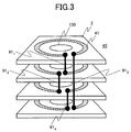
- FIG. 3 is a conceptual rendering illustrating how four element coils (one-turn coils) 41 are laminated to from a two-turn, two-parallel solenoid coil.
- the black circles shown at ends of one-turn coils 41 formed on the upper faces of sapphire substrates 2 represent capacitors formed at the ends of the one-turn coils.
- Numerals 91 1 to 91 4 denote gold thick films that function as connection wires for electrically connecting the capacitors together.
- the two sets of the two one-turn coils 41 connected together through connection wires 91 1 and 91 4 are respectively two-turn coils connected in serial. Both ends of them are connected through connection wires 91 2 and 91 3 to form a two-turn, two-parallel solenoid coil.
- a sample 3 to 10 mm in diameter and 5 to 10 mm in length, is taken as a measuring object.
- the solenoid coil using a superconducting thin film is used to apply a magnetic field to the sample placed in the sample tube 32 and to receive free induction decay (FID) signals.
- FID free induction decay
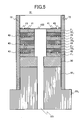
- FIG. 4 is a side view illustrating a cryo probe 31 so constructed that the cryo probe 31 is installed in the direction perpendicular to the static magnetic field.
- the figure illustrates the cryo probe with one side face of a fixed substrate 72 for thermal conduction of sapphire removed.
- FIG. 5 is a sectional view taken along the line B-B (at the center of a hole 100 into which a sample tube 32 is to be passed) of FIG. 4, as viewed in the direction of the arrows.
- An end 55 1 of a cold lead 55 of oxygen free copper to be connected with an end of a cryocooler is formed in the same size as substrates 2.
- a cold head 50 of sapphire is formed on its upper face.
- a substrate 2 4 of sapphire with an element coil 41 formed thereon is disposed on the upper face of the cold head 50.
- a substrate 2 3 of sapphire is disposed on the upper face of the substrate 2 4 with a spacer substrate 73 3 of sapphire in-between.
- a substrate 2 2 of sapphire is disposed on the upper face of the substrate 2 3 with a spacer substrate 73 2 of sapphire in-between; a substrate 2 1 of sapphire is disposed on the upper face of the substrate 2 2 with a spacer substrate 73 1 of sapphire in-between.
- wires 91 1 to 91 4 that connect together the element coils 41 on the substrates 2 and wires for externally leading them out are electrically connected.
- a cut is formed in each spacer substrate 73 in positions corresponding to the wires 91 illustrated in FIG. 2. These cuts are so formed that, when the spacer substrates 73 and the substrates 2 of sapphire are laminated, both can be disposed in parallel with each other. This is the same in the other embodiments.
- a hole 100 through which a sample tube 32 is to be passed is formed in the spacer substrates 73 as well as the substrates 2.
- the probe coil 40 is constructed as a two-turn, two-parallel probe coil. Therefore, the wires connected with the wires 91 2 and 91 3 are connected with the following wires: wires led from the cuts 105 and 106 connecting to a lead-out hole 101 formed in the center of the end 55 1 of the cold lead 55 and the cold head 50.
- a fixed substrate 72 for thermal conduction is provided. The fixed substrate 72 for thermal conduction encircles the end 55 1 of the cold lead 55, the cold head 50, and the laminated portions of the substrates 2 and the spacer substrates 73.
- FIG. 4 the representation of the laminated portions of the substrates 2 and the spacer substrates 73 is omitted for avoiding the complication of the figure.
- FIG. 5 shows the following relation in the form of sectional view for clarification: the relation between the laminated portions, the substrates 2 and the spacer substrates 73, and the fixed substrate 72 for thermal conduction.
- the operation is performed so that both are brought into tight contact and can be welded together by indium.
- indium 43 is placed in the peripheral area of the substrate 2 4 except the plane on which the wires 91 are formed.
- the substrate 2 4 and the spacer substrate 73 3 of sapphire can be bonded together.
- the operation is performed similarly with when the substrate 2 4 is laminated on the end of the cold head 50.
- the operation is performed so that both are brought into tight contact and can be welded together by indium.
- the substrates and the spacer substrates are laminated in succession. Thereafter, the laminated portions of the substrates 2 and the spacer substrates 73, the cold head 50, and the end 55 1 of the cold lead 55 are encircled with the fixed substrate 72 for thermal conduction.
- the thus constructed cryo probe 31 is heated in an oven at 200°C to 300°C for 10 minutes to 30 minutes to fuse the applied indium.
- the fixed substrate 72 for thermal conduction is in contact with the end 55 1 of the cold lead 55 and the cold head 50. Therefore, the fixed substrate 72 for thermal conduction can be cooled down to 5K.
- the spacer substrates 73 are inserted into between the substrates 2 with the element coils 41 formed thereon. The substrates 2 are welded together and the substrates 2 and spacer substrates 73 and the fixed substrate 72 for thermal conduction are welded together by indium. This increases the areas of contact between the peripheral portions of the substrates 2 and spacer substrates 73 and the fixed substrate 72 for thermal conduction, and efficient cooling can be implemented. As a result, the entire solenoid coil is cooled down to approximately 5K, and the stable operation of the probe coil 40 can be accomplished.
- Insertion of the spacer substrates 73 is effective in setting the overall dimensions of the solenoid coil so that the solenoid coil sufficiently covers a sample. Also, it is effective in making the construction robust.
- the fabricated probe coil 40 was evaluated at 600MHz. The result of the evaluation revealed that application of a superconducting thin film enhances the sensitivity by 3.5 times than cases where normal-conducting metal is used.
- YBCO is used for the superconducting thin film material.
- MgB 2 was used for the superconducting thin film material with the same configuration as well, the same result was obtained. It is obvious that, even if Nb, Pb, NbTi, or an alloy of them is used for the superconducting thin film material, the same result will be obtained.
- the fixed substrate 72 for thermal conduction and the spacer substrates 73 sapphire substrates were processed and used.
- the fixed substrate 72 for thermal conduction and the spacer substrates 73 were fabricated using aluminum nitride A1N as well, the same result was obtained.
- FIG. 6A is a top view of a transmission coil formed of an oxygen free copper thin film.
- FIG. 6B is a sectional view taken along the line C-C of FIG. 6A, as viewed in the direction of the arrows.
- Numeral 2 denotes a sapphire substrate, and 95 and 95' denote oxygen free copper thin films.
- the oxygen free copper thin film 95 is formed on the sapphire substrate 2 in the same manner as of the reception coil.
- the substrate 2 is perforated to form a hole 100 through which a sample tube 32 is to be passed.
- the hole in the substrate is formed by laser light irradiation.
- Numerals 92 1 and 92 2 denote wires described later.
- FIG. 7 is a drawing roughly illustrating the configuration of a probe coil 40 formed by combining transmission coils and reception coils.
- the oxygen free copper thin films 95 and 95' formed on the sapphire substrates 2 are so disposed so that the reception coils formed on the laminated substrates 2, described with reference to FIGS. 4 and 5, are sandwiched between their upper faces and lower faces.
- required wires are installed and the probe coil is so constructed that the reception coils are encircled with one-turn saddle coils. More specific description will be given.
- One ends of the oxygen free copper thin films 95 and 95' on the substrate 2 at the uppermost level are connected with one ends of the oxygen free copper thin films 95 and 95' on the substrate 2 at the lowermost level.
- This connection is carried out through wires 92 1 and 92 1 ' on the far side of the figure.
- the other ends of the oxygen free copper thin films 95 and 95' on the substrate 2 at the uppermost level are straightly led to the position of the lowest substrate 2 of reception coil through wires 92 2 and 92 2 '.
- This wiring is carried out on the near side of the figure, and they are connected with each other through a wire 93.
- the other ends of the oxygen free copper thin films 95 and 95' on the substrate 2 at the lowermost level are connected with each other through a wire 94.
- a transmitting signal is applied to between the wire 93 and the wire 94.
- the same reception coils as described with reference to FIG. 3 are used.
- FIG. 8 is a side view of a cryo probe 31 so constructed that the cryo probe is installed in the direction perpendicular to the static magnetic field.
- the figure illustrates the cryo probe 31 formed by combining transmission coils and reception coils.
- the figure illustrates the cryo probe with one side face of a fixed substrate 72 for thermal conduction of sapphire removed.
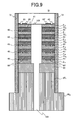
- FIG. 9 is a sectional view taken along the line D-D (at the center of the hole 100 through which a sample tube 32 is to be passed) of FIG. 8, as viewed in the direction of the arrows.
- a substrate 2 6 of sapphire with transmission coils 95 formed thereon is disposed on the upper face of the cold head 50.
- a substrate 2 4 of sapphire with an element coil 41 formed thereon is disposed on the upper face of the substrate 2 6 .
- a substrate 2 3 of sapphire is disposed on the upper face of the substrate 2 4 with a spacer substrate 73 3 of sapphire in-between.
- a substrate 2 2 of sapphire is disposed on the upper face of the substrate 2 3 with a spacer substrate 73 2 of sapphire in-between; and a substrate 2 1 of sapphire is disposed on the upper face of the substrate 2 2 with a spacer substrate 73 1 of sapphire in-between.
- a substrate 2 5 of sapphire with transmission coils 95 formed thereon is disposed on the upper face of the substrate 2 1 .
- wires 92 1 to 92 2 ' that connect together the transmission coils 95 on the substrates and wires for externally leading them out; and wires 91 1 to 91 4 that connect together the element coils 41 of the reception coils and wires for externally lading them out.
- a wire 93 that connects the wires 92 2 and 92 2 ' and a wire 94 that connects together the ends of the transmission coils 95 formed on the substrate 2 6 of sapphire on the near side of the figure are connected with the following wires: wires led from cuts 107 and 108 connecting to a lead-out hole 101 formed in the center of the end 55 1 of the cold lead 55 and the cold head 50.
- wires connected with the wires 91 2 and 91 3 are connected with wires led from cuts 105 and 106 connecting to the lead-out hole 101 formed in the center of the end 55 1 of the cold lead 55 and the cold head 50.
- a fixed substrate 72 for thermal conduction is provided.
- the fixed substrate 72 for thermal conduction encircles the end 55 1 of the cold lead 55, the cold head 50, and the laminated portions of the substrates 2 and the spacer substrates 73.
- FIG. 8 the representation of the laminated portions of the substrates 2 and the spacer substrates 73 is omitted for avoiding the complication of the figure.
- FIG. 9 shows the following relation in the form of sectional view: the relation between the laminated portions, the substrates 2 and the spacer substrates 73, and the fixed substrate 72 for thermal conduction.
- the second embodiment is different from the first embodiment only in that the transmission coils are added at the uppermost and lowermost levels. Therefore, the substrates and spacer substrates are laminated in succession as described with reference to FIG. 5. Thereafter, the laminated portions of the substrates 2 and the spacer substrates 73, the cold head 50, and the end 55 1 of the cold lead 55 are encircled with the fixed substrate 72 for thermal conduction. The thus constructed cryo probe 31 is heated in an oven at 200°C to 300°C for 10 minutes to 30 minutes to fuse the applied indium.
- the fixed substrate 72 for thermal conduction is in contact with the end 55 1 of the cold lead 55 and the cold head 50. Therefore, the fixed substrate 72 for thermal conduction can be cooled down to 5K.
- the spacer substrates 73 are inserted into between the substrates 2 with the element coils 41 formed thereon. The substrates 2 are welded together and the substrates 2 and spacer substrates 73 and the fixed substrate 72 for thermal conduction are welded together by indium. This increases the area of contact between the peripheral portions of the substrates 2 and spacer substrates 73 and the fixed substrate 72 for thermal conduction, and efficient cooling can be implemented. As a result, the entire solenoid coil is cooled down to approximately 5K, and the stable operation of the probe coil 40 can be accomplished.
- the fabricated probe coil 40 was evaluated at 600MHz. The result of the evaluation revealed that application of a superconducting thin film enhances the sensitivity by 3 . 5 times than cases where normal-conducting metal is used. When YBCO was used for the superconducting material with the configuration of the second embodiment as well, the same result was obtained.
- FIG. 10A is a perspective view illustrating a probe coil 40 with a cryo probe 31 installed in parallel with the static magnetic field.
- FIG. 10B is a sectional view taken along the line D-D (at the center of an area where spacer substrates 73 are inserted into a cold head 50) of FIG. 10A, as viewed in the direction of the arrows.
- the configuration of the cryo probe 31 illustrated in FIGS. 10A and 10B is essentially the same as that of the probe coil 40 illustrated in FIG. 4 with respect to portions related to the layered structure of the spacer substrates 73 and the substrates 2.
- the substrate 2 4 is not laminated on the upper face of the cold head 50. Therefore, a spacer substrate 73 5 for transferring cold to the substrate 2 4 is added to the lower face of the substrate 2 4 .
- a substrate 2 3 of sapphire is disposed on the upper face of the substrate 2 4 with a spacer substrate 73 3 of sapphire in-between.
- a substrate 2 2 of sapphire is disposed on the upper face of the substrate 2 3 with a spacer substrate 73 2 of sapphire in-between; and a substrate 2 1 of sapphire is disposed on the upper face of the substrate 2 2 with a spacer substrate 73 1 of sapphire in-between.
- wires 91 1 to 91 4 that connect together the element coils 41 on the substrates 2 and wires for externally leading them out are electrically connected.
- Numeral 43 shown between the substrates denotes fused indium.
- the cryo probe 31 illustrated in FIGS. 10A and 10B is different from the cryo probe 31 illustrated in FIG. 4 in that: the spacer substrates 73 are extended avoiding the wires 91 1 to 91 4 that connect together the element coils 41 on the substrates 2, and inserted into the cold head 50 and fixed there. That is, in order to install the cryo probe 31 in parallel with the static magnetic field, the probe coil 40 is disposed beside the cold head 50 and the cold lead 55. As a result, the cold supplied from a cryocooler is transferred from the cold head 50 to the spacer substrates 73, and then to the substrates 2. Grooves are formed in the cold head 50, and the spacer substrates 73 are inserted into the grooves.
- Wires for externally leading out the wires 91 1 to 91 4 that connect together the element coils 41 on the substrates 2 are led out through a lead-out hole 101 formed in the center of the cold head 50 and the end 55 1 of the cold leader 55.
- the extended portions of the spacer substrates 73 are fixed as follows: the grooves are formed in the cold head 50, and they are inserted into the grooves. In addition, they are welded by indium to enhance the firmness of fixation and the cooling efficiency. Therefore, the spacer substrates 73 can be cooled down to 5K. As a result, the entire solenoid coil is cooled down to approximately 5K, and the stable operation of the probe coil 40 can be accomplished.
- the fabricated probe coil 40 was evaluated at 600MHz.
- the result of the evaluation revealed that as in the first embodiment, application of a superconducting thin film enhances the sensitivity by 3. 5 times than cases where normal-conducting metal is used.
- YBCO was used for the superconducting material with the configuration of the second embodiment as well, the same result was obtained.
- FIG. 11 is a sectional view illustrating a cryo probe 31 so constructed that it is installed in the direction perpendicular to the static magnetic field illustrated in FIG. 9 .
- the figure illustrates the cryo probe 31 formed by combining transmission coils and reception coils.
- a perspective view corresponding to FIG. 10A is omitted.
- the cryo probe 31 illustrated in FIG. 11 is the same as a cryo probe 31 including a probe coil 40 having no transmission coil except the following: the substrate 2 5 with the pattern 95 of upper-face transmission coil formed thereon is provided on the upper face of the sapphire substrate 2 1 of a reception coil; and the substrate 2 6 with the pattern 95 of lower-face transmission coil formed thereon is provided on the lower face of the sapphire substrate 2 4 of a reception coil.
- a spacer substrate 73 4 is provided between the substrate 2 5 with the pattern 95 of upper-face transmission coil formed thereon and the upper face of the sapphire substrate 2 1 of the reception coil.
- a spacer substrate 73 5 is provided between the substrate 2 6 with the pattern 95 of lower-face transmission coil formed thereon and the lower face of the sapphire substrate 2 4 of the reception coil. Further, a spacer substrate 73 6 is provided on the lower face of the substrate 2 6 with the pattern 95 of lower-face transmission coil formed thereon.
- the following wires are led out through a lead-out hole 101 formed in the center of the cold head 50 and the end 55 1 of the cold lead 55: wires for externally leading out wires 91 1 to 91 4 that connect together the element coils 41 on the substrates 2 of reception coils; and wires for externally leading out the wires 93 and 94 of the transmission coils.
- Numeral 43 shown between the substrates denotes fused indium.
- grooves are formed in the cold head 50, and the extended portions of the spacer substrates 73 are inserted into the grooves. In addition, they are additionally welded by indium to enhance the firmness of fixation and the cooling efficiency. Therefore, the spacer substrates 73 can be cooled down to 5K. As a result, the entire solenoid coil is cooled down to approximately 5K, and the stable operation of the probe coil 40 can be accomplished.
- the fabricated probe coil 40 was evaluated at 600MHz. The result of the evaluation revealed that application of a superconducting thin film enhances the sensitivity by 3.5 times than cases where normal-conducting metal is used.
- YBCO was used for the superconducting thin film material.
- MgB 2 was used for the superconducting thin film material with the same configuration as well, the same result was obtained.
- FIG. 12A is a perspective view illustrating a probe coil 40 when a cryo probe 31 is installed in parallel with the static magnetic field.
- FIG. 12B is a sectional view taken along the line D-D (area where spacer substrates 73 are inserted into a cold head 50) of FIG. 12A.
- the configurations of the portions related to the layered structure of the spacer substrates 73 and substrates 2 illustrated in FIGS. 12A and 12B are essentially the same as those in the probe coil 40 illustrated in FIGS. 10A and 10B.
- a spacer substrate 73 6 of sapphire is also laminated on the upper face of the substrate 2 1 .
- the spacer substrates 73 are also extended on the side opposite to the cold head 50, and further, spacers 76 and 77 of sapphire having the same thickness as that of the substrates 2 of sapphire are provided on both sides of the substrates 2.
- the end faces of the spacers 76 agree with the end faces of the spacer substrates 73.
- the spacers 77 are inserted into between the end faces of the substrates 2 and an end face of the cold head 50. When the spacer substrates 73 are laminated, these spacers 76 and 77 are simultaneously laminated on both sides of them.
- Numerals 78 and 79 denote bolts and nuts of polytetrafluoroethylene provided between the spacer substrate 73 6 and the spacer substrate 73 5 and in the laminated portions of the spacers 76 between them.
- Numerals 83 and 84 denote bolts and nuts of polytetrafluoroethylene provided between the spacer substrates 73 6 and the spacer substrate 73 5 and in the laminated portions of the substrates 2.
- Numeral 85 denotes a through hole for the bolts 83.
- the area between the spacer substrate 73 6 and the spacer substrate 73 5 and the laminated portions of the spacers 76 are firmly tightened with the bolts 78 and nuts 79. Further, the area between the spacer substrate 73 6 and the spacer substrate 73 5 and the laminated portions of the substrates 2 are firmly tightened with the bolts 83 and nuts 84. As a result, the mechanical strength of the probe coil 40 can be enhanced.
- the bolts and nuts formed of polytetrafluoroethylene material may be formed of sapphire material or aluminum nitride material, instead.
- the bolts and nuts are formed of polytetrafluoroethylene material, sapphire material, or aluminum nitride material, such a configuration that wires for electrical connection with an external circuit are fixed with these bolts and nuts can be adopted.
- the figures show indium fused between the substrates. However, numeral 43 is given to only one area of fused indium for avoiding the complication of the figures.
- the thus constructed solenoid coil is heated in an oven at 200°C to 300°C for 10 minutes to 30 minutes to fuse the applied indium. Last, the solenoid coil is welded to an end of a cryocooler by indium to obtain the cryo probe 31.
- the spacer substrates 73, substrates 2, spacers 76, and spacers 77 are perforated to form bolt through holes 85.
- the performance of the probe coil 40 in the fifth embodiment is essentially the same as that in the fourth embodiment.
- the thermal conduction effect of the spacers 76 and 77 of sapphire improves the balance of cooling the element coils 41 on the substrates 2. As a result, the performance is further enhanced.
- the fabricated probe coil 40 was evaluated at 600MHz.
- the result of the evaluation revealed that as in the fourth embodiment, application of a superconducting thin film enhances the sensitivity by 3.5 times than cases where normal-conducting metal is used.
- YBCO was used for the superconducting material with the configuration of the fifth embodiment as well, the same result was obtained.
- YBCO was used for the superconducting thin films 41 and sapphire was used for the substrates 2 and the spacer substrates 73.
- MgB 2 is used for the superconducting thin film
- aluminum nitride AlN can be used for the material of the substrates 2.
- the substrates 2 and the spacer substrates 73 can be all formed of AlN.
- FIG. 13 is a sectional view of a cryo probe 31 so constructed that it is installed in parallel with the static magnetic field.
- the figure illustrates the cryo probe 31 formed by combining transmission coils and reception coils.
- a perspective view corresponding to FIG. 12A is omitted.
- the configurations of the portions related to the layered structure of the spacer substrates 73 and substrates 2 illustrated in FIG. 13 are essentially the same as those in the probe coil 40 illustrated in FIG. 11.
- a spacer substrate 73 7 of sapphire is laminated on the upper face of the substrate 2 5 .
- a spacer substrate 73 6 of sapphire is laminated on the lower face of the substrate 2 6 .
- the spacer substrates 73 are also extended on the side opposite to the cold head 50, and further, spacers 76 and 77 of sapphire having the same thickness as that of the substrates 2 are provided on both sides of the substrates 2 of sapphire.
- the end faces of the spacers 76 agree with the end faces of the spacer substrates 73.
- the spacers 77 are inserted into between the end faces of the substrates 2 and an end face of the cold head 50.
- the constructing procedure is also the same as for the fifth embodiment described with reference to FIGS. 12A and 12B.
- Numerals 78 and 79 denote bolts and nuts of polytetrafluoroethylene provided between the spacer substrate 73 7 and the spacer substrate 73 6 and in the laminated portions of the spacers 76 located between them.
- Numerals 83 and 84 denote bolts and nuts of polytetrafluoroethylene provided between the spacer substrate 73 7 and the spacer substrate 73 6 and in the laminated portions of the substrate 2.
- Numeral 85 denotes a through hole for the bolts 83.
- the area between the spacer substrate 73 7 and the spacer substrate 73 6 and the laminated portions of the spacers 76 are firmly tightened with the bolts 78 and nuts 79. Further, the area between the spacer substrate 73 7 and the spacer substrate 73 6 and the laminated portions of the substrates 2 are firmly tightened with the bolts 83 and nuts 84. As a result, the mechanical strength of the probe coil 40 can be enhanced.
- the figure shows indium fused between the substrates. However, numeral 43 is given to only one area of fused indium for avoiding the complication of the figure.
- the thus constructed solenoid coil is heated in an oven at 200°C to 300°C for 10 minutes to 30 minutes to fuse the applied indium. Last, the solenoid coil is welded to an end of a cryocooler by indium to obtain the cryo probe 31.
- the performance of the probe coil 40 in the sixth embodiment is essentially the same as that in the fourth embodiment.
- the thermal conduction effect of the spacers 76 and 77 of sapphire improves the balance of cooling the element coils 41 on the substrates 2. As a result, the performance is further enhanced.
- the fabricated probe coil 40 was evaluated at 600MHz.
- the result of the evaluation revealed that as in the fifth embodiment, application of a superconducting thin film enhances the sensitivity by 3.5 times than cases where normal-conducting metal is used.
- YBCO was used for the superconducting material with the configuration of the sixth embodiment as well, the same result was obtained.
- an NMR measuring apparatus wherein a solenoid superconducting probe coil applicable to split magnets can be inserted in the direction perpendicular to or parallel with the static magnetic field can be realized.
- a superconducting and yet solenoid probe coil can be materialized.
- the thermal noise and the surface resistance can be reduced and the sensitivity can be enhanced through application of a superconducting thin film. Because of the shape of the solenoid coil, the filling factors of samples are enhanced, and this results in the enhanced sensitivity.
- high-sensitivity, high-resolution NMR measurement can be carried out, and protein structures can be analyzed with higher accuracy.
Applications Claiming Priority (1)
| Application Number | Priority Date | Filing Date | Title |
|---|---|---|---|
| JP2004234319A JP4279747B2 (ja) | 2004-08-11 | 2004-08-11 | 核磁気共鳴装置 |
Publications (1)
| Publication Number | Publication Date |
|---|---|
| EP1643261A1 true EP1643261A1 (en) | 2006-04-05 |
Family
ID=35613807
Family Applications (1)
| Application Number | Title | Priority Date | Filing Date |
|---|---|---|---|
| EP05016795A Withdrawn EP1643261A1 (en) | 2004-08-11 | 2005-08-02 | Nuclear magnetic resonance apparatus |
Country Status (3)
| Country | Link |
|---|---|
| US (1) | US7173424B2 (ja) |
| EP (1) | EP1643261A1 (ja) |
| JP (1) | JP4279747B2 (ja) |
Cited By (2)
| Publication number | Priority date | Publication date | Assignee | Title |
|---|---|---|---|---|
| US9739862B2 (en) | 2013-09-26 | 2017-08-22 | Bruker Biospin Ag | DNP apparatus |
| CN108505986A (zh) * | 2018-03-09 | 2018-09-07 | 中国石油天然气股份有限公司 | 核磁共振井下流体识别装置及其井下流体识别探头 |
Families Citing this family (19)
| Publication number | Priority date | Publication date | Assignee | Title |
|---|---|---|---|---|
| CA2309002A1 (en) * | 2000-05-23 | 2001-11-23 | Jonathan Martin Shekter | Digital film grain reduction |
| JP4647984B2 (ja) * | 2004-12-02 | 2011-03-09 | 株式会社日立製作所 | 核磁気共鳴プローブコイル |
| US7456630B2 (en) * | 2005-09-22 | 2008-11-25 | U Chicago Argonne Llc | NMR characterization of thin films |
| WO2007049426A1 (ja) * | 2005-10-25 | 2007-05-03 | Hitachi, Ltd. | 核磁気共鳴プローブおよび核磁気共鳴装置 |
| JP4971685B2 (ja) | 2006-05-25 | 2012-07-11 | 株式会社日立製作所 | 核磁気共鳴プローブコイル |
| JP4861149B2 (ja) * | 2006-12-08 | 2012-01-25 | 株式会社日立製作所 | 核磁気共鳴装置 |
| JP4394716B2 (ja) * | 2007-11-14 | 2010-01-06 | 株式会社日立製作所 | Nmr計測用プローブ |
| WO2010073337A1 (ja) * | 2008-12-25 | 2010-07-01 | 三菱電機株式会社 | 変圧装置 |
| JP5893560B2 (ja) * | 2009-09-21 | 2016-03-23 | タイム メディカル ホールディングス カンパニー リミテッド | 超伝導体rfコイルアレイ |
| KR101038562B1 (ko) | 2010-02-25 | 2011-06-02 | 한국외국어대학교 연구산학협력단 | 고체상 핵자기 공명 프로브 장치 및 그 회로 |
| KR101414779B1 (ko) * | 2010-10-20 | 2014-07-03 | 한국전자통신연구원 | 무선 전력 전송 장치 |
| US9110132B2 (en) * | 2011-08-05 | 2015-08-18 | Chris Chiodo | Electrical and fluid connection system for magnetic imaging |
| JP5890129B2 (ja) * | 2011-09-07 | 2016-03-22 | 株式会社 Jeol Resonance | パルスesr装置 |
| WO2013055823A1 (en) * | 2011-10-10 | 2013-04-18 | Purdue Research Foundation | Afm-coupled microscale radiofrequency probe for magnetic resonance imaging and spectroscopy |
| JP6019515B2 (ja) * | 2012-05-15 | 2016-11-02 | 日本電子株式会社 | Nmr用試料管およびnmr装置 |
| MX2017002939A (es) | 2014-09-05 | 2017-12-07 | Hyperfine Res Inc | Configuracion automatica de un sistema de formacion de imagenes por resonancia magnetica de campo bajo. |
| JP6735619B2 (ja) | 2016-07-20 | 2020-08-05 | 日本電子株式会社 | 磁気共鳴測定用検出コイルの製造方法 |
| WO2024026281A1 (en) * | 2022-07-25 | 2024-02-01 | Rutgers, The State University Of New Jersey | Single crystal sapphire component for angular control during solid state nuclear magnetic resonance measurements |
| CN116679244B (zh) * | 2023-07-27 | 2023-10-17 | 中国科学院上海高等研究院 | 一种快脉冲磁场自动测量装置及方法 |
Citations (4)
| Publication number | Priority date | Publication date | Assignee | Title |
|---|---|---|---|---|
| EP1239297A2 (en) * | 2001-03-09 | 2002-09-11 | Bruker Biospin Corp. | Planar NMR coils with localized field-generating and capacitive elements |
| EP1279967A2 (en) * | 2000-09-30 | 2003-01-29 | Varian, Inc. | Multi-layered, low temperature NMR probe RF coils |
| WO2003029834A1 (en) * | 2001-09-28 | 2003-04-10 | Varian, Inc. | Nmr probe with enhanced power handling ability |
| EP1486793A2 (en) * | 2003-06-10 | 2004-12-15 | Hitachi, Ltd. | Superconducting magnetic resonance r.f. probe coil |
Family Cites Families (10)
| Publication number | Priority date | Publication date | Assignee | Title |
|---|---|---|---|---|
| DE4013111C2 (de) | 1990-04-25 | 1994-05-26 | Spectrospin Ag | HF-Empfangsspulenanordnung für NMR-Spektrometer |
| US5481191A (en) * | 1990-06-29 | 1996-01-02 | Advanced Nmr Systems, Inc. | Shielded gradient coil for nuclear magnetic resonance imaging |
| US5585723A (en) | 1995-03-23 | 1996-12-17 | Conductus, Inc. | Inductively coupled superconducting coil assembly |
| US5572127A (en) * | 1994-08-29 | 1996-11-05 | Conductus, Inc. | Inhomogeneities in static magnetic fields near superconducting coils |
| EP0738897B1 (de) * | 1995-03-25 | 2000-08-09 | Bruker AG | HF-Empfangsspulenanordnung für NMR-Spektrometer |
| DE19733574C2 (de) | 1997-08-02 | 2000-04-06 | Bruker Ag | Supraleitender Hybrid-Resonator für den Empfang für NMR-Signalen |
| US6144204A (en) * | 1997-11-28 | 2000-11-07 | Picker Nordstar Oy | Gradient coils for magnetic resonance meeting |
| DE10018165C2 (de) * | 2000-04-12 | 2003-08-07 | Siemens Ag | Gradientenspule für MR-Anlagen mit direkter Kühlung |
| JP2005087229A (ja) * | 2003-09-12 | 2005-04-07 | Japan Superconductor Technology Inc | スプリット型マグネット及び核磁気共鳴イメージング装置 |
| JP4593255B2 (ja) * | 2004-12-08 | 2010-12-08 | 株式会社日立製作所 | Nmr装置およびnmr計測用プローブ |
-
2004
- 2004-08-11 JP JP2004234319A patent/JP4279747B2/ja not_active Expired - Fee Related
-
2005
- 2005-08-02 EP EP05016795A patent/EP1643261A1/en not_active Withdrawn
- 2005-08-04 US US11/196,279 patent/US7173424B2/en not_active Expired - Fee Related
Patent Citations (4)
| Publication number | Priority date | Publication date | Assignee | Title |
|---|---|---|---|---|
| EP1279967A2 (en) * | 2000-09-30 | 2003-01-29 | Varian, Inc. | Multi-layered, low temperature NMR probe RF coils |
| EP1239297A2 (en) * | 2001-03-09 | 2002-09-11 | Bruker Biospin Corp. | Planar NMR coils with localized field-generating and capacitive elements |
| WO2003029834A1 (en) * | 2001-09-28 | 2003-04-10 | Varian, Inc. | Nmr probe with enhanced power handling ability |
| EP1486793A2 (en) * | 2003-06-10 | 2004-12-15 | Hitachi, Ltd. | Superconducting magnetic resonance r.f. probe coil |
Cited By (2)
| Publication number | Priority date | Publication date | Assignee | Title |
|---|---|---|---|---|
| US9739862B2 (en) | 2013-09-26 | 2017-08-22 | Bruker Biospin Ag | DNP apparatus |
| CN108505986A (zh) * | 2018-03-09 | 2018-09-07 | 中国石油天然气股份有限公司 | 核磁共振井下流体识别装置及其井下流体识别探头 |
Also Published As
| Publication number | Publication date |
|---|---|
| JP2006053020A (ja) | 2006-02-23 |
| US7173424B2 (en) | 2007-02-06 |
| JP4279747B2 (ja) | 2009-06-17 |
| US20060033498A1 (en) | 2006-02-16 |
Similar Documents
| Publication | Publication Date | Title |
|---|---|---|
| US7173424B2 (en) | Nuclear magnetic resonance apparatus | |
| US7138801B2 (en) | NMR spectrometer and NMR probe | |
| US7218115B2 (en) | Superconductor probe coil for NMR apparatus | |
| US6768306B2 (en) | Probe for NMR apparatus using magnesium diboride | |
| US7352186B2 (en) | Nuclear magnetic resonance probe coil | |
| US7619414B2 (en) | NMR probe and NMR spectrometer | |
| EP1666908A1 (en) | Superconducting solenoidal nuclear magnetic resonance probe coil | |
| US20080231277A1 (en) | NMR spectrometer | |
| WO2012155002A1 (en) | Cryogenically cooled whole-body rf coil array and mri system having same | |
| JP4510344B2 (ja) | 低温nmrプローブrfコイル用被覆金属フォイル | |
| JP5006542B2 (ja) | Nmr装置およびnmr計測用プローブ | |
| JP2008026066A (ja) | 核磁気共鳴装置及びnmrプローブコイル |
Legal Events
| Date | Code | Title | Description |
|---|---|---|---|
| PUAI | Public reference made under article 153(3) epc to a published international application that has entered the european phase |
Free format text: ORIGINAL CODE: 0009012 |
|
| AK | Designated contracting states |
Kind code of ref document: A1 Designated state(s): AT BE BG CH CY CZ DE DK EE ES FI FR GB GR HU IE IS IT LI LT LU LV MC NL PL PT RO SE SI SK TR |
|
| AX | Request for extension of the european patent |
Extension state: AL BA HR MK YU |
|
| 17P | Request for examination filed |
Effective date: 20060928 |
|
| 17Q | First examination report despatched |
Effective date: 20061030 |
|
| AKX | Designation fees paid |
Designated state(s): CH DE FR GB LI |
|
| STAA | Information on the status of an ep patent application or granted ep patent |
Free format text: STATUS: THE APPLICATION IS DEEMED TO BE WITHDRAWN |
|
| 18D | Application deemed to be withdrawn |
Effective date: 20070310 |