EP1630845A2 - Plasmaanzeigetafel - Google Patents
Plasmaanzeigetafel Download PDFInfo
- Publication number
- EP1630845A2 EP1630845A2 EP05013856A EP05013856A EP1630845A2 EP 1630845 A2 EP1630845 A2 EP 1630845A2 EP 05013856 A EP05013856 A EP 05013856A EP 05013856 A EP05013856 A EP 05013856A EP 1630845 A2 EP1630845 A2 EP 1630845A2
- Authority
- EP
- European Patent Office
- Prior art keywords
- electrode
- metal
- row
- bus
- separating
- Prior art date
- Legal status (The legal status is an assumption and is not a legal conclusion. Google has not performed a legal analysis and makes no representation as to the accuracy of the status listed.)
- Withdrawn
Links
Images

Classifications
-
- H—ELECTRICITY
- H01—ELECTRIC ELEMENTS
- H01J—ELECTRIC DISCHARGE TUBES OR DISCHARGE LAMPS
- H01J11/00—Gas-filled discharge tubes with alternating current induction of the discharge, e.g. alternating current plasma display panels [AC-PDP]; Gas-filled discharge tubes without any main electrode inside the vessel; Gas-filled discharge tubes with at least one main electrode outside the vessel
- H01J11/10—AC-PDPs with at least one main electrode being out of contact with the plasma
- H01J11/12—AC-PDPs with at least one main electrode being out of contact with the plasma with main electrodes provided on both sides of the discharge space
-
- H—ELECTRICITY
- H01—ELECTRIC ELEMENTS
- H01J—ELECTRIC DISCHARGE TUBES OR DISCHARGE LAMPS
- H01J11/00—Gas-filled discharge tubes with alternating current induction of the discharge, e.g. alternating current plasma display panels [AC-PDP]; Gas-filled discharge tubes without any main electrode inside the vessel; Gas-filled discharge tubes with at least one main electrode outside the vessel
- H01J11/20—Constructional details
- H01J11/22—Electrodes, e.g. special shape, material or configuration
- H01J11/24—Sustain electrodes or scan electrodes
-
- H—ELECTRICITY
- H01—ELECTRIC ELEMENTS
- H01J—ELECTRIC DISCHARGE TUBES OR DISCHARGE LAMPS
- H01J11/00—Gas-filled discharge tubes with alternating current induction of the discharge, e.g. alternating current plasma display panels [AC-PDP]; Gas-filled discharge tubes without any main electrode inside the vessel; Gas-filled discharge tubes with at least one main electrode outside the vessel
- H01J11/20—Constructional details
- H01J11/34—Vessels, containers or parts thereof, e.g. substrates
- H01J11/38—Dielectric or insulating layers
Definitions
- This invention relates to the structure of plasma display panels.
- Fig. 1 is a sectional view illustrating the structure of a surface-discharge-type alternating-current plasma display panel (hereinafter referred to as "PDP").
- PDP surface-discharge-type alternating-current plasma display panel
- Fig. 1 is a sectional view of part of the PDP taken along the column direction (the vertical direction of the panel).
- a plurality of row electrode pairs (X, Y) each extending in the row direction are regularly arranged in the column direction on the back-facing face (the face facing toward the back of the PDP) of the front glass substrate 1 serving as the display surface.
- Each of the row electrodes X and Y constituting a row electrode pair (X, Y) is composed of a bus electrode Xa (Ya) extending in a bar shape in the row direction, and transparent electrodes Xb (Yb) regularly spaced along the bus electrode Xa (Ya) and each extending out therefrom toward its counterpart row electrode Y (X) to face the corresponding transparent electrode Yb (Xb) with a discharge gap g in between.
- the row electrode pairs (X, Y) are covered by the dielectric layer 2.
- the back-facing face of the dielectric layer 2 is covered by an MgO protective layer 3.
- the back glass substrate 4 facing the glass substrate 1 across a discharge space has a front-facing face (the face facing toward the display surface) on which a plurality of column electrodes D are regularly arranged in the row direction, a column-electrode protective layer 5 covers the column electrodes D and an approximate grid-shaped partition wall unit 6 is formed.
- Each of the column electrodes D extends in the column direction along a strip opposite the paired transparent electrodes Xb and Yb of the row electrodes X and Y which are formed on the front glass substrate 1.
- the partition wall unit 6 partitions the discharge space defined between the front glass substrate 1 and the back glass substrate 4 into areas each corresponding to the paired transparent electrodes Xb and Yb facing each other across the discharge gap g to form discharge cells C.
- red-, green- and blue-colored phosphor layers 7 are provided in the individual discharge cells C defined by the partition wall unit 6 and lined up in order in the row direction.
- the discharge cells C are filled with a discharge gas including xenon (Xe).
- a conventional PDP of such a structure is disclosed in Japanese unexamined patent publication 2000-195431.
- the transparent electrodes Xb and Yb of the row electrodes X and Y are formed by patterning. Then, the back-facing face of the front glass substrate 1 is coated with a silver paste (or a silver film is affixed to the back-facing face of the front glass substrate 1) in such a manner as to overlie the proximal ends of the transparent electrodes Xb, Yb to form a bus electrode Xa, Ya.
- a plasma display panel has row electrode pairs formed on one of a pair of substrates facing each other across a discharge space, each row electrode pair being constituted of row electrodes each having a metal electrode portion and transparent electrode portions connected to the metal electrode portion and providing for initiation of a discharge in conjunction with the other row electrode paired therewith.
- the transparent electrode portions are formed on the substrate.
- metal-electrode separating-off dielectric layers are formed on portions of the same substrate, and the metal electrode portion is formed on the metal-electrode separating-off dielectric layer and connected to the transparent electrode portions.
- a PDP has row electrode pairs formed on the back-facing face of a front glass substrate.
- Each of the row electrode pairs is constituted of row electrodes each composed of transparent electrodes that are formed on the back-facing face of the front glass substrate and causing a sustaining discharge in conjunction with its counterpart row electrode, and a silver-made bus electrode that is connected to the transparent electrodes.
- the bus electrode is formed on a bus-electrode separating-off dielectric layer that is formed on a strip portion of the front glass substrate extending along one ends of the transparent electrodes which are located apart from the other row electrode paired therewith.
- the bus-electrode separating-off dielectric layer is formed of a dielectric material not including an alkali element.
- the bus-electrode separating-off dielectric layer formed of the material not including an alkali element separates the silver-made bus electrode and the front glass substrate from each other to prevent direct contact. Accordingly, the reaction between the silver included in the bus electrode and the alkali element included in the front glass substrate does not change the color of the contact portion between the front glass substrate and the bus electrode to yellow, thus overcoming the problem associated with the conventional PDP.
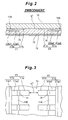
- Figs. 2 and 3 illustrate an embodiment according to the present invention.
- Fig. 2 is a sectional view illustrating the structure of the front glass substrate of the PDP in the embodiment.
- Fig. 3 is a diagram of the front glass substrate of the PDP when viewed from its back-facing face.
- a front glass substrate 10 has a back-facing face on which transparent electrodes X1b in the shape of short strip constituting part of each row electrode X1 each extend in a column direction (the right-left direction in Figs. 2 and 3) and are arranged at regular intervals from each other in a row direction (a direction at right angles to the drawing in Fig. 2 and the vertical direction in Fig. 3).
- bus-electrode separating-off dielectric layers 11A are formed in a bar shape on portions of the back-facing face of the front glass substrate 10 in which the proximal-end portions of the transparent electrodes X1b (the right-end portions in Figs. 2 and 3). Each of the bus-electrode separating-off dielectric layers 11A has a required width in the column direction and extends in the row direction. Each of the bus-electrode separating-off dielectric layers 11A covers the proximal-end portions of the transparent electrodes X1b and a bar-shaped portion of the back-facing face of the front glass substrate 10 including these proximal-end portions.
- the bus-electrode separating-off dielectric layer 11A is partially coated with a silver paste (or alternatively a silver film is affix to part of the dielectric layer 11A) to form a bus electrode X1a.
- Each of the bus electrodes X1a is composed of an electrode body X1a1 extending in a bar shape in the row direction in a position opposite a portion of the back-facing face of the front glass substrate extending alongside the tops of the proximal ends of the transparent electrodes X1b, and a projecting electrodes X1a2 each formed integrally with the electrode body X1a1 to extend out therefrom in a strip opposite a part of the corresponding transparent electrode X1b.
- Each of the projecting electrodes X1a2 of the bus electrode X1a has a leading end Xt curving toward the front glass substrate 10 along the side face of the bus-electrode separating-off dielectric layer 11A and connected to an approximately central portion of the corresponding transparent electrode X1b.
- transparent electrodes Y1b in the shape of short strip constituting part of each row electrode Y1 are spaced at regular intervals from each other in the row direction and each extend in the column direction to face the corresponding transparent electrode X1b of the row electrode X1 across a discharge gap g1.
- bus-electrode separating-off dielectric layer 11A bar-shaped bus-electrode separating-off dielectric layers 11B are each formed on a portion of the back-facing face of the front glass substrate 10 in which the proximal-end portions of the transparent electrodes Y1b (the left-end portions in Figs. 2 and 3) are formed.
- Each of the bus-electrode separating-off dielectric layers 11B has a required width in the column direction and extends in the row direction.
- Each of the bus-electrode separating-off dielectric layers 11B covers the proximal-end portions of the transparent electrodes Y1b and a bar-shaped portion of the back-facing face of the front glass substrate 10 including these proximal-end portions of the transparent electrodes Y1b.
- the bus-electrode separating-off dielectric layer 11B is partially coated with a silver paste (or alternatively a silver film is affixed to a part of the dielectric layer 11B) to form a bus electrode Y1a.
- each of the bus electrodes Y1a is composed of an electrode body Y1a1 extending in a bar shape in the row direction in a position opposite a portion of the back-facing face of the front glass substrate extending alongside the tops of the proximal ends of the transparent electrodes Y1b, and a projecting electrodes Y1a2 each formed integrally with the electrode body Y1a1 to extend out therefrom to oppose the corresponding transparent electrode Y1b.
- Each of the projecting electrodes Y1a2 of the bus electrode Y1a has a leading end Yt curving toward the front glass substrate 10 along the side face of the bus-electrode separating-off dielectric layer 11B and connected to an approximately central portion of the corresponding transparent electrode Y1b.
- the row electrodes X1 and Y1 having the transparent electrodes X1b and Y1b confronting each other across the discharge gaps gl are paired to constitute a row electrode pair (X1, Y1).
- the row electrode pairs (X1, Y1) are regularly arranged in plurality in the column direction (Figs. 2 and 3 show only one of them).
- a dielectric layer 12 is further formed on the back-facing face of the front glass substrate 10 and covers the row electrode pairs (X1, Y1).
- An MgO protective layer 13 is formed on the back-facing face of the dielectric layer 12.
- the bus-electrode separating-off dielectric layers 11A and 11B are formed of a dielectric material such as silica glass which does not include an alkali element by the method of vapor deposition, spattering or the like.
- bus-electrode separating-off dielectric layers 11A and 11B are formed of the same material as the dielectric material not including an alkali element which forms the dielectric layer 12, or of a dielectric material with a lower dielectric constant than that of the dielectric material forming the dielectric layer 12.
- the bus-electrode separating-off dielectric layers 11A and 11B formed of a dielectric material not including an alkali element separate the bus electrodes X1a, Y1a made of silver (Ag) and the front glass substrate 10 from each other to prevent direct contact.
- the silver (Ag) included in the bus electrodes X1a, Y1a and the alkali element included in the front glass substrate 10 are prevented from reacting with each other to change the color of the contact portion between the front glass substrate 10 and the bus electrodes X1a, Y1a to yellow. This prevention in turn prevents a reduction in the display performance of the PDP caused by the color change of the front glass substrate 10.
- the silver paste in the firing process when a silver paste is used to form the bus electrodes of the row electrodes on the front glass substrate, the silver paste may possibly shrink and remains as a residue on the glass substrate.
- the bus electrodes X1a and Y1a are formed on the bus-electrode separating-off dielectric layers 11A and 11B as described in the embodiment, there is no possibility of the silver paste remaining as a residue on the dielectric layer.
Landscapes
- Engineering & Computer Science (AREA)
- Physics & Mathematics (AREA)
- Plasma & Fusion (AREA)
- Chemical & Material Sciences (AREA)
- Materials Engineering (AREA)
- Gas-Filled Discharge Tubes (AREA)
Applications Claiming Priority (1)
| Application Number | Priority Date | Filing Date | Title |
|---|---|---|---|
| JP2004189314A JP2006012661A (ja) | 2004-06-28 | 2004-06-28 | プラズマディスプレイパネル |
Publications (2)
| Publication Number | Publication Date |
|---|---|
| EP1630845A2 true EP1630845A2 (de) | 2006-03-01 |
| EP1630845A3 EP1630845A3 (de) | 2008-01-23 |
Family
ID=35478921
Family Applications (1)
| Application Number | Title | Priority Date | Filing Date |
|---|---|---|---|
| EP05013856A Withdrawn EP1630845A3 (de) | 2004-06-28 | 2005-06-27 | Plasmaanzeigetafel |
Country Status (3)
| Country | Link |
|---|---|
| US (1) | US20050285528A1 (de) |
| EP (1) | EP1630845A3 (de) |
| JP (1) | JP2006012661A (de) |
Family Cites Families (11)
| Publication number | Priority date | Publication date | Assignee | Title |
|---|---|---|---|---|
| JP3163563B2 (ja) * | 1995-08-25 | 2001-05-08 | 富士通株式会社 | 面放電型プラズマ・ディスプレイ・パネル及びその製造方法 |
| JP3739163B2 (ja) * | 1997-03-31 | 2006-01-25 | 三菱電機株式会社 | プラズマディスプレイパネル |
| JP3688114B2 (ja) * | 1998-04-14 | 2005-08-24 | パイオニア株式会社 | プラズマディスプレイパネル |
| WO2000026937A1 (en) * | 1998-10-29 | 2000-05-11 | Mitsubishi Denki Kabushiki Kaisha | Ac plane discharge plasma display panel |
| US6465956B1 (en) * | 1998-12-28 | 2002-10-15 | Pioneer Corporation | Plasma display panel |
| JP3470629B2 (ja) * | 1999-02-24 | 2003-11-25 | 富士通株式会社 | 面放電型プラズマディスプレイパネル |
| TW452812B (en) * | 1999-08-04 | 2001-09-01 | Koninkl Philips Electronics Nv | Plasma display panel |
| JP2001160361A (ja) * | 1999-09-21 | 2001-06-12 | Mitsubishi Electric Corp | プラズマディスプレイパネル用基板及びプラズマディスプレイパネル |
| JP2002075220A (ja) * | 2000-08-28 | 2002-03-15 | Pioneer Electronic Corp | プラズマディスプレイパネル |
| JP2003007216A (ja) * | 2001-06-25 | 2003-01-10 | Nec Corp | プラズマディスプレイパネル及びその製造方法 |
| JP2004079524A (ja) * | 2002-08-02 | 2004-03-11 | Nec Corp | プラズマディスプレイパネル |
-
2004
- 2004-06-28 JP JP2004189314A patent/JP2006012661A/ja active Pending
-
2005
- 2005-06-27 US US11/166,147 patent/US20050285528A1/en not_active Abandoned
- 2005-06-27 EP EP05013856A patent/EP1630845A3/de not_active Withdrawn
Also Published As
| Publication number | Publication date |
|---|---|
| JP2006012661A (ja) | 2006-01-12 |
| US20050285528A1 (en) | 2005-12-29 |
| EP1630845A3 (de) | 2008-01-23 |
Similar Documents
| Publication | Publication Date | Title |
|---|---|---|
| KR101031581B1 (ko) | 플라즈마 디스플레이 패널 및 그 제조 방법 | |
| EP1017081A3 (de) | Plasma Anzeigetafel | |
| KR20010092644A (ko) | 플라즈마 디스플레이 패널 | |
| JPH10321142A (ja) | プラズマディスプレイパネル | |
| US7816867B2 (en) | Plasma display panel | |
| EP1630845A2 (de) | Plasmaanzeigetafel | |
| EP1589558A1 (de) | Plasmaanzeigetafel | |
| US20050264197A1 (en) | Plasma display panel | |
| US20050264206A1 (en) | Plasma display panel | |
| EP1662536B1 (de) | Plasma-Anzeigetafel und Treiberverfahren dafür | |
| JP2008027608A (ja) | プラズマディスプレイパネル | |
| KR100660250B1 (ko) | 플라즈마 디스플레이 패널 | |
| US20050212428A1 (en) | Plasma display panel | |
| KR101082444B1 (ko) | 플라즈마 디스플레이 패널 | |
| EP1791155B1 (de) | Plasmaanzeigetafel | |
| JP2005353418A (ja) | プラズマディスプレイパネル | |
| EP1783800A1 (de) | Plasmaanzeigetafel | |
| US7777402B2 (en) | Plasma display panel improving discharge characteristics in the internal peripheral area thereof | |
| EP1617454A2 (de) | Plasmaanzeigetafel | |
| US20040239250A1 (en) | Plasma display panel | |
| JP2001155644A (ja) | プラズマディスプレイパネル及びその製造方法 | |
| JP2002216642A (ja) | T字型電極と前面隔壁を有するac型pdp | |
| KR20020052420A (ko) | 플라즈마 디스플레이 패널 | |
| JP4661981B2 (ja) | プラズマディスプレイパネルおよびプラズマディスプレイパネルの製造方法 | |
| JP2005149873A (ja) | プラズマディスプレイパネル |
Legal Events
| Date | Code | Title | Description |
|---|---|---|---|
| PUAI | Public reference made under article 153(3) epc to a published international application that has entered the european phase |
Free format text: ORIGINAL CODE: 0009012 |
|
| AK | Designated contracting states |
Kind code of ref document: A2 Designated state(s): AT BE BG CH CY CZ DE DK EE ES FI FR GB GR HU IE IS IT LI LT LU MC NL PL PT RO SE SI SK TR |
|
| AX | Request for extension of the european patent |
Extension state: AL BA HR LV MK YU |
|
| PUAL | Search report despatched |
Free format text: ORIGINAL CODE: 0009013 |
|
| AK | Designated contracting states |
Kind code of ref document: A3 Designated state(s): AT BE BG CH CY CZ DE DK EE ES FI FR GB GR HU IE IS IT LI LT LU MC NL PL PT RO SE SI SK TR |
|
| AX | Request for extension of the european patent |
Extension state: AL BA HR LV MK YU |
|
| STAA | Information on the status of an ep patent application or granted ep patent |
Free format text: STATUS: THE APPLICATION HAS BEEN WITHDRAWN |
|
| 18W | Application withdrawn |
Effective date: 20080211 |