EP1628323B1 - Anode für Sputterbeschichtung - Google Patents
Anode für Sputterbeschichtung Download PDFInfo
- Publication number
- EP1628323B1 EP1628323B1 EP05254602.5A EP05254602A EP1628323B1 EP 1628323 B1 EP1628323 B1 EP 1628323B1 EP 05254602 A EP05254602 A EP 05254602A EP 1628323 B1 EP1628323 B1 EP 1628323B1
- Authority
- EP
- European Patent Office
- Prior art keywords
- anode
- cathode
- sputtering apparatus
- coating
- inner body
- Prior art date
- Legal status (The legal status is an assumption and is not a legal conclusion. Google has not performed a legal analysis and makes no representation as to the accuracy of the status listed.)
- Active
Links
- 238000004544 sputter deposition Methods 0.000 title claims description 57
- 238000000576 coating method Methods 0.000 claims abstract description 82
- 239000011248 coating agent Substances 0.000 claims abstract description 77
- 239000000463 material Substances 0.000 claims abstract description 33
- 238000000034 method Methods 0.000 claims abstract description 24
- 239000000758 substrate Substances 0.000 claims abstract description 17
- 238000009826 distribution Methods 0.000 claims abstract description 11
- 239000007789 gas Substances 0.000 claims description 27
- 238000007667 floating Methods 0.000 claims description 7
- 239000011810 insulating material Substances 0.000 claims description 7
- XLYOFNOQVPJJNP-UHFFFAOYSA-N water Substances O XLYOFNOQVPJJNP-UHFFFAOYSA-N 0.000 claims description 6
- 239000002245 particle Substances 0.000 claims description 5
- 239000000919 ceramic Substances 0.000 claims description 2
- -1 comprising an anode Substances 0.000 claims description 2
- 239000011261 inert gas Substances 0.000 claims 1
- 238000000151 deposition Methods 0.000 abstract description 10
- 238000001755 magnetron sputter deposition Methods 0.000 abstract description 5
- 230000008878 coupling Effects 0.000 abstract description 4
- 238000010168 coupling process Methods 0.000 abstract description 4
- 238000005859 coupling reaction Methods 0.000 abstract description 4
- 230000007547 defect Effects 0.000 abstract description 4
- 238000004519 manufacturing process Methods 0.000 abstract 2
- VYPSYNLAJGMNEJ-UHFFFAOYSA-N Silicium dioxide Chemical compound O=[Si]=O VYPSYNLAJGMNEJ-UHFFFAOYSA-N 0.000 description 14
- 230000008569 process Effects 0.000 description 13
- 239000010408 film Substances 0.000 description 11
- XKRFYHLGVUSROY-UHFFFAOYSA-N Argon Chemical compound [Ar] XKRFYHLGVUSROY-UHFFFAOYSA-N 0.000 description 9
- 238000005546 reactive sputtering Methods 0.000 description 7
- 230000008021 deposition Effects 0.000 description 6
- 238000013461 design Methods 0.000 description 6
- 235000012239 silicon dioxide Nutrition 0.000 description 6
- 239000000377 silicon dioxide Substances 0.000 description 6
- RYGMFSIKBFXOCR-UHFFFAOYSA-N Copper Chemical compound [Cu] RYGMFSIKBFXOCR-UHFFFAOYSA-N 0.000 description 5
- 238000013459 approach Methods 0.000 description 5
- 229910052786 argon Inorganic materials 0.000 description 5
- 238000001816 cooling Methods 0.000 description 5
- 229910052802 copper Inorganic materials 0.000 description 5
- 239000010949 copper Substances 0.000 description 5
- 230000009977 dual effect Effects 0.000 description 5
- PNEYBMLMFCGWSK-UHFFFAOYSA-N aluminium oxide Inorganic materials [O-2].[O-2].[O-2].[Al+3].[Al+3] PNEYBMLMFCGWSK-UHFFFAOYSA-N 0.000 description 4
- 230000000694 effects Effects 0.000 description 4
- 239000012777 electrically insulating material Substances 0.000 description 4
- 239000012212 insulator Substances 0.000 description 4
- 150000002500 ions Chemical class 0.000 description 4
- 229910001220 stainless steel Inorganic materials 0.000 description 4
- 239000010935 stainless steel Substances 0.000 description 4
- 239000013077 target material Substances 0.000 description 4
- 230000008859 change Effects 0.000 description 3
- 230000007423 decrease Effects 0.000 description 3
- 239000003989 dielectric material Substances 0.000 description 3
- 229910052581 Si3N4 Inorganic materials 0.000 description 2
- 229910052681 coesite Inorganic materials 0.000 description 2
- 229910052906 cristobalite Inorganic materials 0.000 description 2
- 238000005137 deposition process Methods 0.000 description 2
- 230000005684 electric field Effects 0.000 description 2
- 238000005516 engineering process Methods 0.000 description 2
- 230000003628 erosive effect Effects 0.000 description 2
- 238000002474 experimental method Methods 0.000 description 2
- 230000004907 flux Effects 0.000 description 2
- 238000011065 in-situ storage Methods 0.000 description 2
- 238000012423 maintenance Methods 0.000 description 2
- 230000003287 optical effect Effects 0.000 description 2
- 238000001552 radio frequency sputter deposition Methods 0.000 description 2
- 238000005507 spraying Methods 0.000 description 2
- 229910052682 stishovite Inorganic materials 0.000 description 2
- 229910052905 tridymite Inorganic materials 0.000 description 2
- 0 C*=CC=CCN Chemical compound C*=CC=CCN 0.000 description 1
- 241001264766 Callistemon Species 0.000 description 1
- 239000004809 Teflon Substances 0.000 description 1
- 229920006362 Teflon® Polymers 0.000 description 1
- 238000009825 accumulation Methods 0.000 description 1
- 239000010405 anode material Substances 0.000 description 1
- QVGXLLKOCUKJST-UHFFFAOYSA-N atomic oxygen Chemical compound [O] QVGXLLKOCUKJST-UHFFFAOYSA-N 0.000 description 1
- 230000015572 biosynthetic process Effects 0.000 description 1
- 230000015556 catabolic process Effects 0.000 description 1
- 239000010406 cathode material Substances 0.000 description 1
- 238000004140 cleaning Methods 0.000 description 1
- 150000001875 compounds Chemical class 0.000 description 1
- 239000004020 conductor Substances 0.000 description 1
- 238000011109 contamination Methods 0.000 description 1
- 230000002939 deleterious effect Effects 0.000 description 1
- 238000010586 diagram Methods 0.000 description 1
- 238000010292 electrical insulation Methods 0.000 description 1
- 238000010438 heat treatment Methods 0.000 description 1
- 238000009413 insulation Methods 0.000 description 1
- 238000010849 ion bombardment Methods 0.000 description 1
- 238000005259 measurement Methods 0.000 description 1
- 230000007246 mechanism Effects 0.000 description 1
- 229910044991 metal oxide Inorganic materials 0.000 description 1
- 150000004706 metal oxides Chemical class 0.000 description 1
- 239000000615 nonconductor Substances 0.000 description 1
- 229910052760 oxygen Inorganic materials 0.000 description 1
- 239000001301 oxygen Substances 0.000 description 1
- 238000010422 painting Methods 0.000 description 1
- 238000007750 plasma spraying Methods 0.000 description 1
- 239000000376 reactant Substances 0.000 description 1
- 230000009467 reduction Effects 0.000 description 1
- 239000004065 semiconductor Substances 0.000 description 1
- 229910052710 silicon Inorganic materials 0.000 description 1
- 239000010703 silicon Substances 0.000 description 1
- HQVNEWCFYHHQES-UHFFFAOYSA-N silicon nitride Chemical compound N12[Si]34N5[Si]62N3[Si]51N64 HQVNEWCFYHHQES-UHFFFAOYSA-N 0.000 description 1
- 239000007787 solid Substances 0.000 description 1
- 241000894007 species Species 0.000 description 1
- 230000003595 spectral effect Effects 0.000 description 1
- 238000005477 sputtering target Methods 0.000 description 1
- 238000012360 testing method Methods 0.000 description 1
- 239000010409 thin film Substances 0.000 description 1
- 238000001771 vacuum deposition Methods 0.000 description 1
Images


Classifications
-
- H—ELECTRICITY
- H01—ELECTRIC ELEMENTS
- H01J—ELECTRIC DISCHARGE TUBES OR DISCHARGE LAMPS
- H01J37/00—Discharge tubes with provision for introducing objects or material to be exposed to the discharge, e.g. for the purpose of examination or processing thereof
- H01J37/32—Gas-filled discharge tubes
- H01J37/34—Gas-filled discharge tubes operating with cathodic sputtering
-
- H—ELECTRICITY
- H01—ELECTRIC ELEMENTS
- H01J—ELECTRIC DISCHARGE TUBES OR DISCHARGE LAMPS
- H01J37/00—Discharge tubes with provision for introducing objects or material to be exposed to the discharge, e.g. for the purpose of examination or processing thereof
- H01J37/32—Gas-filled discharge tubes
- H01J37/32431—Constructional details of the reactor
- H01J37/32532—Electrodes
- H01J37/32541—Shape
-
- H—ELECTRICITY
- H01—ELECTRIC ELEMENTS
- H01J—ELECTRIC DISCHARGE TUBES OR DISCHARGE LAMPS
- H01J37/00—Discharge tubes with provision for introducing objects or material to be exposed to the discharge, e.g. for the purpose of examination or processing thereof
- H01J37/32—Gas-filled discharge tubes
- H01J37/34—Gas-filled discharge tubes operating with cathodic sputtering
- H01J37/3411—Constructional aspects of the reactor
- H01J37/3438—Electrodes other than cathode
Definitions
- This invention relates to a sputtering apparatus and method for depositing films on a substrate, and more particularly to a reactive magnetron sputtering device and technique for depositing materials onto substrates in which the deposited films have predictive thickness distribution and in which the apparatus can operate continuously and repeatedly for very long periods.
- ions are usually created by collisions between gas atoms and electrons in a glow discharge.
- the ions are accelerated into the target cathode by an electric field causing atoms of the target material to be ejected from the cathode surface.
- a substrate is placed in a suitable location so that it intercepts a portion of the ejected atoms. Thus, a coating of target material is deposited on the surface of the substrate.
- Sputter coating is a widely used technique for depositing a thin film of material on a substrate.
- Sputtering is the physical ejection of material from a target as a result of gas ion bombardment of the target.
- DC sputtering positive ions from a plasma discharge formed between an anode and a target cathode are attracted to and strike the target cathode, dislodging atoms from the target surface of the cathode thereby providing atoms. Some of the dislodged atoms impinge on the surface of the substrate and form a coating.
- a gaseous species is also present at the substrate surface and reacts with, and in some embodiments combines with, the atoms from the target surface to form the desired coating material.
- the sputtered material is also deposited on any other surface exposed to the sputtered atoms.
- the coating is an electrically insulating material, such as a metal oxide
- the build up of the material on other parts of the sputtering apparatus can cause problems.
- the build up of an insulating coating on the anode interferes with the ability of the anode to remove electrons from the plasma, as required to maintain the plasma's charge balance. This destabilizes the plasma and interferes with deposition control.
- RF sputtering is a less efficient, less controllable, slower and more expensive process than DC sputtering.
- the DC voltage applied between the target cathode and the anode ionizes the argon to form a plasma, and the positively charged argon ions are attracted to the negatively charged target.
- the ions strike the target with a substantial energy and cause target atoms or atomic clusters to be sputtered from the target. Some of the sputtered target material strikes and deposits on the wafer or substrate material to be coated, thereby forming a film.
- the cathode In order to attain increased deposition rates and lower operating pressures, magnetically enhanced targets have been used.
- the cathode includes an array of permanent magnets arranged in a closed loop and mounted in a fixed position in relation to the flat target plate. The resulting magnetic field causes the electrons to travel in a closed loop, commonly referred to as a "race track", which establishes the path or region along which sputtering or erosion of the target material takes place.
- a magnetic field confines the glow discharge plasma and increases the path length of the electrons moving under the influence of the electric field. This results in an increase in the gas atom-electron collision probability thereby leading to a much higher sputtering rate than that obtained without the use of magnetic confinement. Furthermore, the sputtering process can be accomplished at a much lower gas pressure.
- a reactant gas forms a compound with the material which is sputtered from the target plate.
- the target plate is silicon and the reactive gas is oxygen, silicon dioxide is formed on the surface of the substrate.
- silicon dioxide is a good insulator, a film thick enough to cause arcing is rapidly formed on the target surface in areas outside of the race track and on other nearby surfaces, e.g. on electrically grounded dark space shields.
- Silicon dioxide is known to be one of the most difficult dielectric films to deposit by magnetron reactive sputtering because of this characteristic. The arcing associated with silicon dioxide has prevented planar magnetron reactive sputtering from being efficiently utilized to deposit high quality silicon dioxide films.
- One aspect of this invention provides a coated cathode having its sides and bottom surface coated with a dielectric to lessen or prevent arcing.
- planar and cylindrical magnetrons in either reactive or non-reactive sputtering is that films deposited by sputtering have not achieved the high degree of uniformity or repeatability required for many precision applications.
- Anode plates and ring designs described by J.R. Doyle, et al., in J.Vac. Sci. Technol. A12, 886 (1994 ) are the most widely used design for anodes.
- the anode is in close proximity to the cathode to enable a sufficient coupling of the anode-to-cathode plasma.
- the gas inlet is close to the target surface to increase the target pressure locally.
- the anode surface is also close to that location which increases the plasma coupling and reduces the anode voltage.
- Unfortunately these types of anodes can't be positioned too far behind the cathode, because the electrons have to cross magnetic field lines on route to the anode which adds a high resistance and increases the anode voltage.
- having the anode close to the cathode surface increases the anode's susceptibility to being coated with sputtered material thereby making the anode unstable.
- the size of the anodes has to be relatively large to work at a reasonably low voltage.
- the large size leads to an uneven contamination of the anode surface and to a change in sputter distribution.
- a large anode has to be accommodated within the coating chamber where space is typically lacking.
- a small filament-like anode is another form of prior art anode.
- This anode requires relatively high voltages, for example, greater than 70 V, which typically leads to undesirable sputtering of surfaces at or near the anode.
- the anode has to be positioned very close to the cathode for sufficient coupling. Additionally, major changes to the magnetron generally have to be made by way of shunting the magnetic fields close to the anode.
- anode Since the anode is generally close to the target, it is exposed to coating material. In practice, in many prior art systems, anodes have to be exchanged or cleaned at frequent, regular intervals. Even when the anode is out of a direct line of sight of the sputtered material flux, the anode becomes coated due to gas scattering of coating material.
- the provision of such an anode leads to a more stable sputtering process, especially for very thick coatings, and reduces or eliminates the maintenance of the anode. This reduces the cycle time and labor costs in coating substrates.
- a sputtering apparatus as defined by claim 1.
- an anode 10 is shown in the form of a container or vessel having conductive walls of copper or stainless steel 12 having an opening 14 at a first end for communicating with a vacuum chamber to which it is directly coupled.
- the copper or stainless steel walls define the inside of the container vessel or inner body of the container.
- the outside walls of the container are referred to hereafter as the outer body.
- the outer body may be coated with a suitable coating so as to be electrically insulated.
- water cooling pipes 16 are shown substantially around the anode for maintaining the temperature of the anode in operation.
- a gas inlet port 18 is shown for providing a conduit into which gas may enter the anode cavity to pressurize the anode.
- a ground cover 21 is placed around the anode and cooling pipes and is at ground potential.
- the anode is pressurized with argon gas which promotes the formation of plasma in the presence of a suitable ignition voltage and maintenance voltage thereafter.
- the anode 10 is essentially a conducting container, which in a preferred embodiment is mounted onto the vacuum chamber; alternatively, it may reside within the vacuum chamber.
- the anode shown in Fig. 1a was designed to function with a low anode voltage and little or no arcing. A low anode voltage of approximately 30 volts is preferred to reduce process variation.
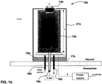
- FIG. 1b an anode similar to the one shown in Fig. 1a is shown, wherein the entire anode body is shown disposed within a vacuum coating chamber and wherein the opening 14b having a diameter d 0 for communicating with the target cathode plasma within the vacuum chamber.
- Water cooling tubing 16b is shown having inlet and outlet ports entering and exiting from outside the vacuum chamber.
- the Ar-gas port 18b is shown to communicate with the anode and supply the anode with gas from outside the vacuum chamber.
- An insulator 19b ensures the anode is electrically insulated from the chamber wall and a power supply is shown to provide a voltage difference between the anode and cathode or cathode material within the chamber.
- Fig. le shows an alternative embodiment wherein an anode having copper walls 12c have an opening 14c at a different location which is at the side of the cylinder.
- the anode can be mounted within or external to the vacuum chamber. Water cooling pipes 16c, and Ar gas port 18c are provided.
- circuitry which allows three distinct modes of electrical operation of the anode 70.
- the switch 72 allows switchable selection between 'floating', 'grounded', and 'biased' operation.
- floating operation the potential of the anode relative to ground is self adjusting.
- the anode voltage depends upon the plasma impedance.
- the typical anode voltage is measured to be between +20V and +55V, whereas the cathode voltage can be anywhere between -300V and -700V, depending upon which materials are coated and which process parameters are used.
- a resistor is provided between the ground and the anode to protect the system in case of a catastrophic electrical breakdown or arc.
- the anode In grounded operation mode the anode is connected to chamber ground. To be the preferred return path for the electrons, the anode needs to have superior conductivity over other grounded chamber components. Feeding process gas into the anode decreases the plasma impedance to the anode.
- anode potential relative to ground is determined by a power supply.
- a voltage range of +20 to +55V makes the anode the preferred return path for electrons while maintaining a constant and repeatable operation.
- the chamber pressure is below 2 mTorr.
- a high pressure at the anode is achieved by reducing the orifice or opening 14 of the anode 10 and feeding the process gas into the anode via the inlet port 18. Since small orifices constrict the plasma leading to a reduction in electrical conductivity and thus to an increase of the anode voltage, it was discovered that an optimum opening has an area of about 20 cm 2 and is preferably round. This relationship is depicted in Fig. 5 .
- the anode can be made of a plurality of conducting materials.
- the impact of the anode material on the anode voltage is illustrated in Fig. 6 .
- This graph illustrates that copper results in a 2 V lower anode voltage than stainless steel.
- the anode 10 shown in Fig. 1 is electrically insulated from the grounded chamber wall by way of an insulating material 19 shown. This is important since it is preferred for the anode to be able to have a free floating voltage which will typically be greater than that of the grounded chamber wall.
- electrical and water feed-through connections and gas lines 18 can be mounted from the outside.
- the thickness of the walls have to be sufficient to withstand the atmospheric pressure; in the instance when the anode serves as an internal anode the anode can be quite thin as long as the anode does not become too highly electrically resistive.
- the anode In operation the anode can be pressurized to more than 3 mTorr. It is expected that this anode 10 can run in nearly continuous operation for extended periods of time; experiments have been carried out running this anode for more than 2000 hours continuously without having to take the anode 10 out of service to be cleaned or changed, and it is believed that it is possible to operate the anode for more than 10000 hours of continuous operation.
- the insulation of the outside can be a coating on the anode body, but alternatively can be an additional cover 21b as shown in Fig. 1b .
- the cover 21 can be grounded or floating.
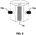
- FIG. 8 illustrates one of many possible anode configurations for elongated cathodes as used in a MetaModeTM configuration.
- two anodes 72a, 72b are positioned symmetrically at the sides of a long planar Si cathode 74.
- the instant invention is believed to be applicable to this and other such in-line coating systems; for example it is believed that the use of multiple anodes could be used in such in-line coating systems.
- the hollow anode described heretofore in accordance with this invention could increase the performance of the anode arrangement scheme described in this publication by Sieck.
- anodes along the cathode which either are controlled electrically or wherein the gas flow through the anode is adjusted through the anode cavity to control the sputter distribution along the length of the cathode.
- Such adjustments could be done in-situ during a coating run, for example, with a feedback loop from in-situ spectral measurements.
- Fig. 10a a plan view is shown of a coating machine with an elongated cathode 101 having anodes 102 through 107 disposed about the anode.
- Fig 10b is an end view of Fig. 10a wherein the elongated cathode 101 is a cylindrical cathode having independent gas inlets 120a and 120b.
- Fig. 10 is an end view of Fig. 10 a wherein the cathode is a planar cathode.
- cathode In addition to providing a novel and inventive anode, an ever-increasing demand for low defect concentration in coated devices such as optical filters, mirrors, and semiconductor circuits requires a cathode that will have little or no arcing at the sputtering target. At present commercially available cathodes and also cathode designs described in prior art lack this important feature, especially when the deposition rate is being kept high.
- cathode for used in sputter coating of a material onto one or more substrates.
- This cathode can be used in conjunction with the described anode that essentially reduces any arcing to near zero or acceptable levels that do not have deleterious effects on the substrates being coated.
- the cathode together with the anode described heretofore provides a coating system that is highly reliable and requires very little down time.
- the combination of the anode and cathode disclosed here provides a coating mechanism that is unsurpassed by other known coating chambers.
- US patent 5,334,298 provides a cathode and shield where the marginal areas of the target lying outside the erosion zone are covered over by an extension of the dark space shield.
- the dark space shield is electrically floating and is separated from the target by a gap which is so large that no plasma can ignite between the target and the dark space shield.
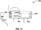
- a cathode 130 is shown with an anode 140, wherein gas is fed into the chamber, away from the cathode through the anode.
- This avoids high pressure close to the cathode where the magnetic field is high.
- the anode opening is at least 2 inches away from the cathode to enable a uniform pressure distribution over the target area.
- the anode voltage has been found to be insensitive to the distance between anode and cathode. Since this embodiment does not require a dark space shield, this eliminates coating flakes falling on the targets from a dark-space shield which typically extends into the flux of sputtered particles.
- the sides of the cathode are electrically insulated.
- the electrical insulation 142 can be accomplished by the use of insulating materials or through application of an insulating coating.
- the dielectric coating can be a dense alumina applied through a plasma spray coating process.
- the cathode can be insulated by way of being coated with a layer of KaptonTM tape. Alternatively the cathode can be mounted on an insulating material such as TeflonTM or a ceramic. Alternatively sides of the cathode can be exposed to normal atmosphere where air becomes the electrical insulator.
- Combinations of above mentioned techniques can be used to insulate the cathode. Furthermore, extending the body of the cathode laterally so as to lessen the magnetic field that extends beyond the cathode body reduces the arcing. By insulating an extended cathode by plasma spraying alumina on its side and insulating the bottom with a TeflonTM plate it is possible to reduce the arc rate from >100 arcs/s to ⁇ 0.1 arcs/s for the same deposition rate. This is a very inexpensive yet effective solution to the problem of unwanted arcing.
- the cathode in accordance with this invention can be used for metallic and dielectric coatings.
- the cathode can be driven with any electrical mode (RF, DC, pulsed DC, MF, dual cathode-AC, single cathode AC).
- coating within this specification to depict an electric insulating coating is to include spraying on a coating of electrically insulating material such as alumina, or painting on such a coating, or applying a coating of electrically insulating tape such as KaptonTM tape; alternatively and less preferably, coating the cathode sides or bottom with Teflon plates is also possible, however in this instance the plates must be adjacent to and contacting the conductive sidewalls of the cathode.
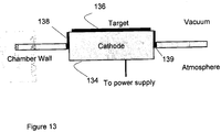
- a cathode 136 is shown partially disposed within the interior of the vacuum chamber under vacuum with the target facing inward to the interior of the chamber 136 and wherein a remaining portion is shown outside the vacuum chamber under atmospheric pressure.
- the cathode 136 is inserted through an opening in the wall of the chamber and is sealed with a seal 139 so that vacuum can be maintained.
- the side walls of the portion inside the vacuum chamber are coated with an electrically insulating material 138.
Landscapes
- Physics & Mathematics (AREA)
- Engineering & Computer Science (AREA)
- Plasma & Fusion (AREA)
- Chemical & Material Sciences (AREA)
- Analytical Chemistry (AREA)
- Physical Vapour Deposition (AREA)
- Magnetic Heads (AREA)
- Thin Magnetic Films (AREA)
- Coating By Spraying Or Casting (AREA)
- Drying Of Semiconductors (AREA)
- Apparatuses And Processes For Manufacturing Resistors (AREA)
Claims (19)
- Eine Sputtervorrichtung zur Verwendung beim Sputtern eines Materials, beinhaltend eine Anode und eine Beschichtungskammer, die eine Kathode und ein mit dem Sputtermaterial zu beschichtendes Substrat enthält,
dadurch gekennzeichnet, dass die Anode (10) einen Behälter mit einem elektrisch leitfähigen Innenkörper (12), einem Außenkörper, einem Anodenhohlraum innerhalb des elektrisch leitfähigen Innenkörpers und einer Öffnung (14) an einem Ende des elektrisch leitfähigen Innenkörpers definiert, um mit der Beschichtungskammer in Verbindung zu stehen, um zuzulassen, dass geladene Teilchen zwischen dem elektrisch leitfähigen Innenkörper und der Kathode innerhalb der Beschichtungskammer strömen, und
wobei der elektrisch leitfähige Innenkörper mit einer Spannungsquelle gekoppelt ist, um zwischen dem Sputtermaterial und dem leitfähigen Innenkörper eine Spannungsdifferenz bereitzustellen; und
wobei die Öffnung wesentlich kleiner als ein Umfang des Behälters ist und so bemessen ist, dass Beschichtungsmaterial im Wesentlichen daran gehindert wird, sich in dem Behälter abzulagern. - Sputtervorrichtung gemäß Anspruch 1, wobei der Behälter einen Einlasskanal (18) zum Aufnehmen eines Inertgases zum Zünden von Plasma in Gegenwart einer ausreichenden Spannung, die zwischen dem elektrisch leitfähigen Innenkörper (12) und der Kathode angelegt wird, aufweist.
- Sputtervorrichtung gemäß Anspruch 1, wobei die Anode (10) außerhalb der Beschichtungskammer angeordnet und physikalisch damit gekoppelt ist, so dass die Öffnung des Behälters der Beschichtungskammer zugewandt und dieser gegenüber offen ist.
- Sputtervorrichtung gemäß Anspruch 1, wobei der Außenkörper des Behälters ein erstes Material beinhaltet, das sich von dem Innenkörper des Behälters unterscheidet, und wobei das erste Material ein isolierendes Material ist.
- Sputtervorrichtung gemäß Anspruch 1, wobei der elektrisch leitfähige Innenkörper (12) mit einem Schalter (72) gekoppelt ist, um den elektrisch leitfähigen Innenkörper wahlweise potenzialfrei, vorgespannt oder geerdet zu machen.
- Sputtervorrichtung gemäß Anspruch 1, wobei die Anode (10) ortsfest mit einer Außenseite der Beschichtungskammer gekoppelt ist, so dass im Betrieb während des Beschichtens die Anode als ein leitfähiges Behältnis dient, und wobei geladene Teilchen zwischen der Kathode in der Beschichtungskammer und der Innenseite des Behälters zum Beschichten eines in der Beschichtungskammer angeordneten Substrats mit dem Material strömen.
- Sputtervorrichtung gemäß Anspruch 1, wobei die Öffnung (14) eine Fläche von > 10 cm2 aufweist.
- Sputtervorrichtungsanode gemäß Anspruch 1, wobei Gas- und/oder Wasserleitungen außerhalb der Beschichtungskammer an der Anode (10) angebracht sind.
- Sputtervorrichtung gemäß Anspruch 1, wobei der Anodenhohlraum im Querschnitt im Wesentlichen zylindrisch oder sphärisch ist.
- Sputtervorrichtung gemäß Anspruch 1, wobei eine Oberfläche des elektrisch leitfähigen Innenkörpers (12) mindestens 300 cm2 beträgt.
- Sputtervorrichtung gemäß Anspruch 2, wobei der Druck im Anodenhohlraum der gleiche ist wie in der Beschichtungskammer.
- Sputtervorrichtung gemäß Anspruch 2, wobei der Druck im Anodenhohlraum mindestens 20 % über dem Druck in der Beschichtungskammer liegt.
- Sputtervorrichtung gemäß Anspruch 2, wobei der Druck im Anodenhohlraum mindestens zweimal über dem Druck in der Beschichtungskammer liegt.
- Sputtervorrichtung gemäß Anspruch 1, wobei die Anode (10) wassergekühlt ist.
- Sputtervorrichtung gemäß Anspruch 1, ferner umfassend eine zweite Anode, die einen Behälter mit einem elektrisch leitfähigen Innenkörper, einem Außenkörper und einer Öffnung definiert, um zuzulassen, dass geladene Teilchen zwischen dem elektrisch leitfähigen Innenkörper und der Kathode innerhalb der Beschichtungskammer strömen, und wobei der elektrisch leitfähige Innenkörper der zweiten Anode mit einer Spannungsquelle zum Bereitstellen einer Spannungsdifferenz zwischen der Kathode und dem elektrisch leitfähigen Innenkörper der zweiten Anode gekoppelt ist.
- Sputtervorrichtung gemäß Anspruch 15, wobei die erste Anode (10) und die zweite Anode mit einer gleichen linearen Kathode elektrisch gekoppelt sind.
- Sputtervorrichtung gemäß Anspruch 1, wobei die Kathode in der Nähe von und in Verbindung mit der Anode (10) angeordnet ist, wobei die Seiten der Kathode elektrisch isoliert sind.
- Sputtervorrichtung gemäß Anspruch 17, wobei die Seiten der Kathode mit einer dielektrischen Beschichtung, Isolierband, einer Teflon™-Beschichtung oder -Platte und keramischen Platten oder Kombinationen davon beschichtet sind.
- Ein Verfahren zum Steuern der Verteilung von Beschichtungsmaterial in einer Sputtervorrichtung gemäß Anspruch 1, bei der es sich um eine Gleichstromsputtervorrichtung handelt, wobei das Verfahren das elektrische Schalten der Anoden und/oder das unabhängige Einstellen des Gasstroms auf Behälter verschiedener Anoden zum Steuern der Sputterverteilung von Beschichtungsmaterial beinhaltet.
Applications Claiming Priority (3)
| Application Number | Priority Date | Filing Date | Title |
|---|---|---|---|
| US60321104P | 2004-08-20 | 2004-08-20 | |
| US11/074,249 US20060049041A1 (en) | 2004-08-20 | 2005-03-07 | Anode for sputter coating |
| US11/177,465 US7879209B2 (en) | 2004-08-20 | 2005-07-08 | Cathode for sputter coating |
Publications (3)
| Publication Number | Publication Date |
|---|---|
| EP1628323A2 EP1628323A2 (de) | 2006-02-22 |
| EP1628323A3 EP1628323A3 (de) | 2009-04-22 |
| EP1628323B1 true EP1628323B1 (de) | 2017-03-29 |
Family
ID=35722363
Family Applications (2)
| Application Number | Title | Priority Date | Filing Date |
|---|---|---|---|
| EP05254602.5A Active EP1628323B1 (de) | 2004-08-20 | 2005-07-23 | Anode für Sputterbeschichtung |
| EP05255082A Active EP1628324B8 (de) | 2004-08-20 | 2005-08-17 | Magnetron-Sputteranlage |
Family Applications After (1)
| Application Number | Title | Priority Date | Filing Date |
|---|---|---|---|
| EP05255082A Active EP1628324B8 (de) | 2004-08-20 | 2005-08-17 | Magnetron-Sputteranlage |
Country Status (7)
| Country | Link |
|---|---|
| US (2) | US7879209B2 (de) |
| EP (2) | EP1628323B1 (de) |
| JP (2) | JP4907124B2 (de) |
| CN (2) | CN1737188B (de) |
| AT (1) | ATE492025T1 (de) |
| DE (1) | DE602005025293D1 (de) |
| ES (1) | ES2626641T3 (de) |
Families Citing this family (34)
| Publication number | Priority date | Publication date | Assignee | Title |
|---|---|---|---|---|
| JP4669831B2 (ja) * | 2006-11-17 | 2011-04-13 | 株式会社アルバック | イオンビーム源及びこれを備えた成膜装置 |
| CN101240410B (zh) * | 2007-02-07 | 2010-11-24 | 鸿富锦精密工业(深圳)有限公司 | 溅镀装置 |
| EP1970465B1 (de) * | 2007-03-13 | 2013-08-21 | JDS Uniphase Corporation | Verfahren und Kathodenzerstäubungssystem zum Auftragen einer aus einer Mischung von Materialien zusammengesetzten Schicht mit einer im Voraus bestimmten Brechzahl |
| JP5311263B2 (ja) * | 2007-11-01 | 2013-10-09 | エリコン・トレーディング・アクチェンゲゼルシャフト,トリュープバッハ | 被処理面を作製するための方法および真空プラズマ源 |
| US20090169751A1 (en) * | 2007-12-27 | 2009-07-02 | Exatec Llc | Multi-Pass Vacuum Coating Systems |
| US20090294017A1 (en) * | 2008-05-30 | 2009-12-03 | Precision Photonics Corporation | Optical contacting enabled by thin film dielectric interface |
| US20100272964A1 (en) * | 2008-05-30 | 2010-10-28 | Precision Photonics Corporation - Photonics | Optical Contacting Enabled by Thin Film Dielectric Interface |
| US20090294050A1 (en) * | 2008-05-30 | 2009-12-03 | Precision Photonics Corporation | Optical contacting enhanced by hydroxide ions in a non-aqueous solution |
| JP2010285316A (ja) * | 2009-06-12 | 2010-12-24 | Konica Minolta Opto Inc | 金型の製造方法、ガラスゴブの製造方法及びガラス成形体の製造方法 |
| JP5619666B2 (ja) * | 2010-04-16 | 2014-11-05 | ジェイディーエス ユニフェイズ コーポレーションJDS Uniphase Corporation | マグネトロン・スパッタリング・デバイスで使用するためのリング・カソード |
| US9502222B2 (en) * | 2010-04-16 | 2016-11-22 | Viavi Solutions Inc. | Integrated anode and activated reactive gas source for use in magnetron sputtering device |
| US8647437B2 (en) * | 2010-05-31 | 2014-02-11 | Ci Systems (Israel) Ltd. | Apparatus, tool and methods for depositing annular or circular wedge coatings |
| RU2450086C2 (ru) * | 2010-06-08 | 2012-05-10 | Федеральное государственное бюджетное образовательное учреждение высшего профессионального образования "Национальный исследовательский институт "МЭИ" (ФГБОУ ВПО "НИУ МЭИ") | Способ нанесения нанокомпозитного покрытия на плоские поверхности детали и устройство для его реализации (варианты) |
| DE102010038603B4 (de) * | 2010-07-29 | 2016-06-02 | Trumpf Huettinger Sp. Z O. O. | DC-Plasmaanordnung |
| DK2509100T3 (da) * | 2011-04-06 | 2019-11-04 | Viavi Solutions Inc | Integreret anode og aktiveret reaktiv gaskilde til anvendelse i en magnetron-sputtering-enhed |
| JP6023722B2 (ja) * | 2011-12-22 | 2016-11-09 | キヤノンアネルバ株式会社 | SrRuO3膜の成膜方法 |
| JP6244103B2 (ja) | 2012-05-04 | 2017-12-06 | ヴァイアヴィ・ソリューションズ・インコーポレイテッドViavi Solutions Inc. | 反応性スパッタ堆積のための方法および反応性スパッタ堆積システム |
| TWI756606B (zh) | 2012-07-16 | 2022-03-01 | 美商唯亞威方案公司 | 光學濾波器及感測器系統 |
| CN103602954B (zh) * | 2013-11-06 | 2016-02-24 | 深圳市华星光电技术有限公司 | 用于磁控溅射阳极棒的支撑件及包括其的磁控溅射装置 |
| WO2016032444A1 (en) * | 2014-08-26 | 2016-03-03 | Applied Materials, Inc. | Vacuum deposition apparatus and method of operating thereof |
| EP3091561B1 (de) | 2015-05-06 | 2019-09-04 | safematic GmbH | Sputtereinheit |
| EP3091101B1 (de) | 2015-05-06 | 2018-10-17 | safematic GmbH | Beschichtungseinheit |
| CN104988465B (zh) * | 2015-06-29 | 2017-10-13 | 信利(惠州)智能显示有限公司 | 磁控溅射装置阳极部件 |
| US9923007B2 (en) | 2015-12-29 | 2018-03-20 | Viavi Solutions Inc. | Metal mirror based multispectral filter array |
| US9960199B2 (en) | 2015-12-29 | 2018-05-01 | Viavi Solutions Inc. | Dielectric mirror based multispectral filter array |
| EP3279364B1 (de) * | 2016-08-03 | 2021-10-06 | IHI Hauzer Techno Coating B.V. | Vorrichtung zur beschichtung von substraten |
| US10168459B2 (en) * | 2016-11-30 | 2019-01-01 | Viavi Solutions Inc. | Silicon-germanium based optical filter |
| CN106950933B (zh) * | 2017-05-02 | 2019-04-23 | 中江联合(北京)科技有限公司 | 质量一致性控制方法及装置、计算机存储介质 |
| US10802185B2 (en) | 2017-08-16 | 2020-10-13 | Lumentum Operations Llc | Multi-level diffractive optical element thin film coating |
| US10712475B2 (en) | 2017-08-16 | 2020-07-14 | Lumentum Operations Llc | Multi-layer thin film stack for diffractive optical elements |
| CN107365968B (zh) * | 2017-08-24 | 2019-09-17 | 武汉华星光电半导体显示技术有限公司 | 一种溅镀装置及溅镀系统 |
| CN111286712B (zh) * | 2018-12-10 | 2022-05-17 | 苏州能讯高能半导体有限公司 | 一种靶材溅镀设备以及靶材溅镀系统 |
| DE102019119664A1 (de) * | 2019-07-19 | 2021-01-21 | Infineon Technologies Ag | Abtasten eines Drehwinkels |
| CN111041434B (zh) * | 2020-03-17 | 2020-06-19 | 上海陛通半导体能源科技股份有限公司 | 用于沉积绝缘膜的物理气相沉积设备 |
Citations (4)
| Publication number | Priority date | Publication date | Assignee | Title |
|---|---|---|---|---|
| US3616452A (en) * | 1967-06-22 | 1971-10-26 | Alsacienne De Construction Ato | Production of deposits by cathode sputtering |
| US3916034A (en) * | 1971-05-21 | 1975-10-28 | Hitachi Ltd | Method of transporting substances in a plasma stream to and depositing it on a target |
| EP0308680A1 (de) * | 1987-09-21 | 1989-03-29 | THELEN, Alfred, Dr. | Vorrichtung zum Kathodenzerstäuben |
| WO2001098553A1 (en) * | 2000-06-19 | 2001-12-27 | Chemfilt R & D Ab | Pulsed highly ionized magnetron sputtering |
Family Cites Families (51)
| Publication number | Priority date | Publication date | Assignee | Title |
|---|---|---|---|---|
| US1015438A (en) | 1910-09-22 | 1912-01-23 | Corp Of Maschinenfabrik Moenus A G | Belt-sewing machine. |
| US3514391A (en) | 1967-05-05 | 1970-05-26 | Nat Res Corp | Sputtering apparatus with finned anode |
| US3528906A (en) * | 1967-06-05 | 1970-09-15 | Texas Instruments Inc | Rf sputtering method and system |
| US4131533A (en) * | 1977-12-30 | 1978-12-26 | International Business Machines Corporation | RF sputtering apparatus having floating anode shield |
| US4169031A (en) | 1978-01-13 | 1979-09-25 | Polyohm, Inc. | Magnetron sputter cathode assembly |
| US4222345A (en) | 1978-11-30 | 1980-09-16 | Optical Coating Laboratory, Inc. | Vacuum coating apparatus with rotary motion assembly |
| US4250009A (en) | 1979-05-18 | 1981-02-10 | International Business Machines Corporation | Energetic particle beam deposition system |
| US5766738A (en) | 1979-12-28 | 1998-06-16 | Flex Products, Inc. | Paired optically variable article with paired optically variable structures and ink, paint and foil incorporating the same and method |
| US4318796A (en) | 1980-07-15 | 1982-03-09 | Murata Manufacturing Co., Ltd. | Sputtering apparatus |
| US4351697A (en) * | 1982-01-04 | 1982-09-28 | Western Electric Company, Inc. | Printed wiring boards |
| US4569745A (en) * | 1982-10-05 | 1986-02-11 | Fujitsu Limited | Sputtering apparatus |
| JPH0627323B2 (ja) * | 1983-12-26 | 1994-04-13 | 株式会社日立製作所 | スパツタリング方法及びその装置 |
| US4478702A (en) | 1984-01-17 | 1984-10-23 | Ppg Industries, Inc. | Anode for magnetic sputtering apparatus |
| JPS6110239A (ja) | 1984-06-25 | 1986-01-17 | Nec Kansai Ltd | 半導体製造装置 |
| DE3427587A1 (de) | 1984-07-26 | 1986-02-06 | Leybold-Heraeus GmbH, 5000 Köln | Zerstaeubungseinrichtung fuer katodenzerstaeubungsanlagen |
| EP0173164B1 (de) | 1984-08-31 | 1988-11-09 | Hitachi, Ltd. | Aufstäuben mittels Mikrowellen |
| WO1989003584A1 (en) | 1987-10-14 | 1989-04-20 | Unisearch Limited | Multi-electrode vacuum processing chamber |
| DE3835153A1 (de) | 1988-10-15 | 1990-04-26 | Leybold Ag | Vorrichtung zum aetzen von substraten durch eine glimmentladung |
| JP2592311B2 (ja) | 1988-10-19 | 1997-03-19 | 富士写真フイルム株式会社 | 光磁気記録媒体の製造方法及び製造装置 |
| DE4025077A1 (de) * | 1990-08-08 | 1992-02-20 | Leybold Ag | Magnetronkathode |
| RU2008501C1 (ru) | 1990-10-09 | 1994-02-28 | Валерий Андреевич Попов | Воздухоочиститель для двигателя внутреннего сгорания |
| DE69226725T2 (de) | 1991-05-29 | 1999-02-18 | Kabushiki Kaisha Kobe Seiko Sho (Kobe Steel, Ltd.), Kobe | Beschichtungsanlage mittels Kathodenzerstäubung und Methode zur Steuerung derselben |
| IT1249440B (it) * | 1991-08-14 | 1995-02-23 | Ist Nazionale Fisica Nucleare | Metodo e dispositivo per la deposizione tramite spruzzamento catodico di films sottili superconduttori di niobio su cavita' risonanti a quarto d'onda in rame per l'accellerazione di ioni pesanti. |
| US5525199A (en) * | 1991-11-13 | 1996-06-11 | Optical Corporation Of America | Low pressure reactive magnetron sputtering apparatus and method |
| DE4137483A1 (de) * | 1991-11-14 | 1993-05-19 | Leybold Ag | Kathode zum beschichten eines substrats |
| DE4201551C2 (de) | 1992-01-22 | 1996-04-25 | Leybold Ag | Zerstäubungskathode |
| EP0556449B1 (de) | 1992-02-21 | 1997-03-26 | Hashimoto Forming Industry Co., Ltd. | Lackierung mit magnetisch hergestelltem Muster und lackiertes Produkt mit magnetisch hergestelltem Muster |
| DE4237517A1 (de) * | 1992-11-06 | 1994-05-11 | Leybold Ag | Vorrichtung zum Beschichten eines Substrats, insbesondere mit elektrisch nichtleitenden Schichten |
| DE4306611B4 (de) | 1993-03-03 | 2004-04-15 | Unaxis Deutschland Holding Gmbh | Vorrichtung zur Oberflächenbehandlung von Substraten durch Plasmaeinwirkung |
| CA2123479C (en) | 1993-07-01 | 1999-07-06 | Peter A. Sieck | Anode structure for magnetron sputtering systems |
| US5507931A (en) * | 1993-12-30 | 1996-04-16 | Deposition Technologies, Inc. | Sputter deposition process |
| US5573596A (en) | 1994-01-28 | 1996-11-12 | Applied Materials, Inc. | Arc suppression in a plasma processing system |
| JP2748886B2 (ja) | 1995-03-31 | 1998-05-13 | 日本電気株式会社 | プラズマ処理装置 |
| DE29505497U1 (de) | 1995-03-31 | 1995-06-08 | Balzers Hochvakuum GmbH, 65205 Wiesbaden | Beschichtungsstation |
| DE19513691A1 (de) * | 1995-04-11 | 1996-10-17 | Leybold Ag | Vorrichtung zum Aufbringen dünner Schichten auf ein Substrat |
| US5795448A (en) | 1995-12-08 | 1998-08-18 | Sony Corporation | Magnetic device for rotating a substrate |
| JP3537269B2 (ja) * | 1996-05-21 | 2004-06-14 | アネルバ株式会社 | マルチチャンバースパッタリング装置 |
| US5736021A (en) | 1996-07-10 | 1998-04-07 | Applied Materials, Inc. | Electrically floating shield in a plasma reactor |
| US6190513B1 (en) | 1997-05-14 | 2001-02-20 | Applied Materials, Inc. | Darkspace shield for improved RF transmission in inductively coupled plasma sources for sputter deposition |
| US6117279A (en) * | 1998-11-12 | 2000-09-12 | Tokyo Electron Limited | Method and apparatus for increasing the metal ion fraction in ionized physical vapor deposition |
| US6207472B1 (en) | 1999-03-09 | 2001-03-27 | International Business Machines Corporation | Low temperature thin film transistor fabrication |
| JP4656744B2 (ja) * | 2000-03-09 | 2011-03-23 | キヤノンアネルバ株式会社 | スパッタリング装置 |
| WO2002019379A1 (en) | 2000-08-28 | 2002-03-07 | Institute For Plasma Research | Device and process for producing dc glow discharge |
| JP4592949B2 (ja) * | 2000-12-27 | 2010-12-08 | キヤノンアネルバ株式会社 | マグネトロンスパッタリング装置 |
| US20020160194A1 (en) | 2001-04-27 | 2002-10-31 | Flex Products, Inc. | Multi-layered magnetic pigments and foils |
| US6841238B2 (en) | 2002-04-05 | 2005-01-11 | Flex Products, Inc. | Chromatic diffractive pigments and foils |
| US20030116432A1 (en) * | 2001-12-26 | 2003-06-26 | Applied Materials, Inc. | Adjustable throw reactor |
| US7645510B2 (en) | 2002-09-13 | 2010-01-12 | Jds Uniphase Corporation | Provision of frames or borders around opaque flakes for covert security applications |
| US7241489B2 (en) | 2002-09-13 | 2007-07-10 | Jds Uniphase Corporation | Opaque flake for covert security applications |
| US7166199B2 (en) * | 2002-12-18 | 2007-01-23 | Cardinal Cg Company | Magnetron sputtering systems including anodic gas distribution systems |
| US7785456B2 (en) | 2004-10-19 | 2010-08-31 | Jds Uniphase Corporation | Magnetic latch for a vapour deposition system |
-
2005
- 2005-07-08 US US11/177,465 patent/US7879209B2/en active Active
- 2005-07-23 ES ES05254602.5T patent/ES2626641T3/es active Active
- 2005-07-23 EP EP05254602.5A patent/EP1628323B1/de active Active
- 2005-08-17 DE DE602005025293T patent/DE602005025293D1/de active Active
- 2005-08-17 EP EP05255082A patent/EP1628324B8/de active Active
- 2005-08-17 AT AT05255082T patent/ATE492025T1/de not_active IP Right Cessation
- 2005-08-17 US US11/205,398 patent/US8163144B2/en active Active
- 2005-08-18 JP JP2005237830A patent/JP4907124B2/ja active Active
- 2005-08-19 JP JP2005238264A patent/JP5048229B2/ja active Active
- 2005-08-19 CN CN200510090898.7A patent/CN1737188B/zh active Active
- 2005-08-22 CN CN200510092825.1A patent/CN1737190B/zh active Active
Patent Citations (4)
| Publication number | Priority date | Publication date | Assignee | Title |
|---|---|---|---|---|
| US3616452A (en) * | 1967-06-22 | 1971-10-26 | Alsacienne De Construction Ato | Production of deposits by cathode sputtering |
| US3916034A (en) * | 1971-05-21 | 1975-10-28 | Hitachi Ltd | Method of transporting substances in a plasma stream to and depositing it on a target |
| EP0308680A1 (de) * | 1987-09-21 | 1989-03-29 | THELEN, Alfred, Dr. | Vorrichtung zum Kathodenzerstäuben |
| WO2001098553A1 (en) * | 2000-06-19 | 2001-12-27 | Chemfilt R & D Ab | Pulsed highly ionized magnetron sputtering |
Also Published As
| Publication number | Publication date |
|---|---|
| CN1737188B (zh) | 2011-12-14 |
| US8163144B2 (en) | 2012-04-24 |
| EP1628323A3 (de) | 2009-04-22 |
| ATE492025T1 (de) | 2011-01-15 |
| DE602005025293D1 (de) | 2011-01-27 |
| EP1628324B1 (de) | 2010-12-15 |
| JP2006057184A (ja) | 2006-03-02 |
| US20060049042A1 (en) | 2006-03-09 |
| CN1737188A (zh) | 2006-02-22 |
| JP2006057181A (ja) | 2006-03-02 |
| CN1737190B (zh) | 2012-05-23 |
| ES2626641T3 (es) | 2017-07-25 |
| US7879209B2 (en) | 2011-02-01 |
| CN1737190A (zh) | 2006-02-22 |
| JP4907124B2 (ja) | 2012-03-28 |
| EP1628324A2 (de) | 2006-02-22 |
| EP1628323A2 (de) | 2006-02-22 |
| EP1628324B8 (de) | 2011-01-26 |
| JP5048229B2 (ja) | 2012-10-17 |
| EP1628324A3 (de) | 2007-07-04 |
| US20060070877A1 (en) | 2006-04-06 |
Similar Documents
| Publication | Publication Date | Title |
|---|---|---|
| EP1628323B1 (de) | Anode für Sputterbeschichtung | |
| US6197165B1 (en) | Method and apparatus for ionized physical vapor deposition | |
| JP5346178B2 (ja) | プラズマの発生及びスパッタのためのコイル | |
| US5213672A (en) | Sputtering apparatus with a rotating target | |
| US5800688A (en) | Apparatus for ionized sputtering | |
| KR100239818B1 (ko) | 기초재의 반응코팅을 위한 방법과 장치 | |
| US20160326635A1 (en) | Remote Arc Discharge Plasma Assisted Processes | |
| US6413387B1 (en) | Cathode arc source for metallic and dielectric coatings | |
| US20020163289A1 (en) | Hall-current ion source | |
| JP5619666B2 (ja) | マグネトロン・スパッタリング・デバイスで使用するためのリング・カソード | |
| EP0070982B1 (de) | Zerstäubungsvorrichtung | |
| EP0978138A1 (de) | Verfahren und gereat zur ionisierter materialzerstauebung | |
| US20060049041A1 (en) | Anode for sputter coating | |
| KR20000068062A (ko) | 내부 유도 코일 안테나 및 전기적 전도성 챔버 벽을 갖는 rf 플라즈마 에칭 반응기 | |
| KR102616067B1 (ko) | Pvd 스퍼터링 증착 챔버의 경사형 마그네트론 | |
| US6506287B1 (en) | Overlap design of one-turn coil | |
| EP0818801A2 (de) | Plasmabehandlungsgerät | |
| US8500973B2 (en) | Anode for sputter coating | |
| WO2000003414A1 (en) | Feedthrough overlap coil | |
| US6475353B1 (en) | Apparatus and method for sputter depositing dielectric films on a substrate | |
| US6495000B1 (en) | System and method for DC sputtering oxide films with a finned anode | |
| CA3103016A1 (en) | Single beam plasma source | |
| KR100779247B1 (ko) | 금속 무늬 판재의 제조 방법 |
Legal Events
| Date | Code | Title | Description |
|---|---|---|---|
| PUAI | Public reference made under article 153(3) epc to a published international application that has entered the european phase |
Free format text: ORIGINAL CODE: 0009012 |
|
| AK | Designated contracting states |
Kind code of ref document: A2 Designated state(s): AT BE BG CH CY CZ DE DK EE ES FI FR GB GR HU IE IS IT LI LT LU LV MC NL PL PT RO SE SI SK TR |
|
| AX | Request for extension of the european patent |
Extension state: AL BA HR MK YU |
|
| PUAL | Search report despatched |
Free format text: ORIGINAL CODE: 0009013 |
|
| AK | Designated contracting states |
Kind code of ref document: A3 Designated state(s): AT BE BG CH CY CZ DE DK EE ES FI FR GB GR HU IE IS IT LI LT LU LV MC NL PL PT RO SE SI SK TR |
|
| AX | Request for extension of the european patent |
Extension state: AL BA HR MK YU |
|
| RIC1 | Information provided on ipc code assigned before grant |
Ipc: C23C 14/35 20060101ALI20090319BHEP Ipc: C23C 14/34 20060101ALI20090319BHEP Ipc: H01J 37/34 20060101AFI20051201BHEP |
|
| 17P | Request for examination filed |
Effective date: 20091019 |
|
| AKX | Designation fees paid |
Designated state(s): AT BE BG CH CY CZ DE DK EE ES FI FR GB GR HU IE IS IT LI LT LU LV MC NL PL PT RO SE SI SK TR |
|
| 17Q | First examination report despatched |
Effective date: 20100114 |
|
| RAP1 | Party data changed (applicant data changed or rights of an application transferred) |
Owner name: VIAVI SOLUTIONS INC. |
|
| GRAP | Despatch of communication of intention to grant a patent |
Free format text: ORIGINAL CODE: EPIDOSNIGR1 |
|
| INTG | Intention to grant announced |
Effective date: 20161019 |
|
| STAA | Information on the status of an ep patent application or granted ep patent |
Free format text: STATUS: GRANT OF PATENT IS INTENDED |
|
| GRAS | Grant fee paid |
Free format text: ORIGINAL CODE: EPIDOSNIGR3 |
|
| GRAA | (expected) grant |
Free format text: ORIGINAL CODE: 0009210 |
|
| STAA | Information on the status of an ep patent application or granted ep patent |
Free format text: STATUS: THE PATENT HAS BEEN GRANTED |
|
| AK | Designated contracting states |
Kind code of ref document: B1 Designated state(s): AT BE BG CH CY CZ DE DK EE ES FI FR GB GR HU IE IS IT LI LT LU LV MC NL PL PT RO SE SI SK TR |
|
| REG | Reference to a national code |
Ref country code: GB Ref legal event code: FG4D |
|
| REG | Reference to a national code |
Ref country code: CH Ref legal event code: EP |
|
| REG | Reference to a national code |
Ref country code: CH Ref legal event code: NV Representative=s name: MURGITROYD AND COMPANY, CH |
|
| REG | Reference to a national code |
Ref country code: AT Ref legal event code: REF Ref document number: 880472 Country of ref document: AT Kind code of ref document: T Effective date: 20170415 |
|
| REG | Reference to a national code |
Ref country code: IE Ref legal event code: FG4D |
|
| REG | Reference to a national code |
Ref country code: DE Ref legal event code: R096 Ref document number: 602005051615 Country of ref document: DE |
|
| REG | Reference to a national code |
Ref country code: SE Ref legal event code: TRGR |
|
| REG | Reference to a national code |
Ref country code: NL Ref legal event code: FP |
|
| REG | Reference to a national code |
Ref country code: ES Ref legal event code: FG2A Ref document number: 2626641 Country of ref document: ES Kind code of ref document: T3 Effective date: 20170725 |
|
| REG | Reference to a national code |
Ref country code: FR Ref legal event code: PLFP Year of fee payment: 13 |
|
| PG25 | Lapsed in a contracting state [announced via postgrant information from national office to epo] |
Ref country code: GR Free format text: LAPSE BECAUSE OF FAILURE TO SUBMIT A TRANSLATION OF THE DESCRIPTION OR TO PAY THE FEE WITHIN THE PRESCRIBED TIME-LIMIT Effective date: 20170630 Ref country code: LT Free format text: LAPSE BECAUSE OF FAILURE TO SUBMIT A TRANSLATION OF THE DESCRIPTION OR TO PAY THE FEE WITHIN THE PRESCRIBED TIME-LIMIT Effective date: 20170329 Ref country code: FI Free format text: LAPSE BECAUSE OF FAILURE TO SUBMIT A TRANSLATION OF THE DESCRIPTION OR TO PAY THE FEE WITHIN THE PRESCRIBED TIME-LIMIT Effective date: 20170329 |
|
| REG | Reference to a national code |
Ref country code: AT Ref legal event code: MK05 Ref document number: 880472 Country of ref document: AT Kind code of ref document: T Effective date: 20170329 |
|
| PG25 | Lapsed in a contracting state [announced via postgrant information from national office to epo] |
Ref country code: LV Free format text: LAPSE BECAUSE OF FAILURE TO SUBMIT A TRANSLATION OF THE DESCRIPTION OR TO PAY THE FEE WITHIN THE PRESCRIBED TIME-LIMIT Effective date: 20170329 Ref country code: BG Free format text: LAPSE BECAUSE OF FAILURE TO SUBMIT A TRANSLATION OF THE DESCRIPTION OR TO PAY THE FEE WITHIN THE PRESCRIBED TIME-LIMIT Effective date: 20170629 |
|
| PG25 | Lapsed in a contracting state [announced via postgrant information from national office to epo] |
Ref country code: CZ Free format text: LAPSE BECAUSE OF FAILURE TO SUBMIT A TRANSLATION OF THE DESCRIPTION OR TO PAY THE FEE WITHIN THE PRESCRIBED TIME-LIMIT Effective date: 20170329 Ref country code: AT Free format text: LAPSE BECAUSE OF FAILURE TO SUBMIT A TRANSLATION OF THE DESCRIPTION OR TO PAY THE FEE WITHIN THE PRESCRIBED TIME-LIMIT Effective date: 20170329 Ref country code: RO Free format text: LAPSE BECAUSE OF FAILURE TO SUBMIT A TRANSLATION OF THE DESCRIPTION OR TO PAY THE FEE WITHIN THE PRESCRIBED TIME-LIMIT Effective date: 20170329 Ref country code: IT Free format text: LAPSE BECAUSE OF FAILURE TO SUBMIT A TRANSLATION OF THE DESCRIPTION OR TO PAY THE FEE WITHIN THE PRESCRIBED TIME-LIMIT Effective date: 20170329 Ref country code: EE Free format text: LAPSE BECAUSE OF FAILURE TO SUBMIT A TRANSLATION OF THE DESCRIPTION OR TO PAY THE FEE WITHIN THE PRESCRIBED TIME-LIMIT Effective date: 20170329 Ref country code: SK Free format text: LAPSE BECAUSE OF FAILURE TO SUBMIT A TRANSLATION OF THE DESCRIPTION OR TO PAY THE FEE WITHIN THE PRESCRIBED TIME-LIMIT Effective date: 20170329 |
|
| PG25 | Lapsed in a contracting state [announced via postgrant information from national office to epo] |
Ref country code: PT Free format text: LAPSE BECAUSE OF FAILURE TO SUBMIT A TRANSLATION OF THE DESCRIPTION OR TO PAY THE FEE WITHIN THE PRESCRIBED TIME-LIMIT Effective date: 20170731 Ref country code: PL Free format text: LAPSE BECAUSE OF FAILURE TO SUBMIT A TRANSLATION OF THE DESCRIPTION OR TO PAY THE FEE WITHIN THE PRESCRIBED TIME-LIMIT Effective date: 20170329 Ref country code: IS Free format text: LAPSE BECAUSE OF FAILURE TO SUBMIT A TRANSLATION OF THE DESCRIPTION OR TO PAY THE FEE WITHIN THE PRESCRIBED TIME-LIMIT Effective date: 20170729 |
|
| REG | Reference to a national code |
Ref country code: DE Ref legal event code: R097 Ref document number: 602005051615 Country of ref document: DE |
|
| PG25 | Lapsed in a contracting state [announced via postgrant information from national office to epo] |
Ref country code: DK Free format text: LAPSE BECAUSE OF FAILURE TO SUBMIT A TRANSLATION OF THE DESCRIPTION OR TO PAY THE FEE WITHIN THE PRESCRIBED TIME-LIMIT Effective date: 20170329 |
|
| PLBE | No opposition filed within time limit |
Free format text: ORIGINAL CODE: 0009261 |
|
| STAA | Information on the status of an ep patent application or granted ep patent |
Free format text: STATUS: NO OPPOSITION FILED WITHIN TIME LIMIT |
|
| 26N | No opposition filed |
Effective date: 20180103 |
|
| GBPC | Gb: european patent ceased through non-payment of renewal fee |
Effective date: 20170723 |
|
| PG25 | Lapsed in a contracting state [announced via postgrant information from national office to epo] |
Ref country code: GB Free format text: LAPSE BECAUSE OF NON-PAYMENT OF DUE FEES Effective date: 20170723 |
|
| PG25 | Lapsed in a contracting state [announced via postgrant information from national office to epo] |
Ref country code: SI Free format text: LAPSE BECAUSE OF FAILURE TO SUBMIT A TRANSLATION OF THE DESCRIPTION OR TO PAY THE FEE WITHIN THE PRESCRIBED TIME-LIMIT Effective date: 20170329 |
|
| PG25 | Lapsed in a contracting state [announced via postgrant information from national office to epo] |
Ref country code: LU Free format text: LAPSE BECAUSE OF NON-PAYMENT OF DUE FEES Effective date: 20170723 |
|
| REG | Reference to a national code |
Ref country code: FR Ref legal event code: PLFP Year of fee payment: 14 |
|
| PG25 | Lapsed in a contracting state [announced via postgrant information from national office to epo] |
Ref country code: HU Free format text: LAPSE BECAUSE OF FAILURE TO SUBMIT A TRANSLATION OF THE DESCRIPTION OR TO PAY THE FEE WITHIN THE PRESCRIBED TIME-LIMIT; INVALID AB INITIO Effective date: 20050723 Ref country code: MC Free format text: LAPSE BECAUSE OF FAILURE TO SUBMIT A TRANSLATION OF THE DESCRIPTION OR TO PAY THE FEE WITHIN THE PRESCRIBED TIME-LIMIT Effective date: 20170329 |
|
| PG25 | Lapsed in a contracting state [announced via postgrant information from national office to epo] |
Ref country code: CY Free format text: LAPSE BECAUSE OF NON-PAYMENT OF DUE FEES Effective date: 20170329 |
|
| PG25 | Lapsed in a contracting state [announced via postgrant information from national office to epo] |
Ref country code: TR Free format text: LAPSE BECAUSE OF FAILURE TO SUBMIT A TRANSLATION OF THE DESCRIPTION OR TO PAY THE FEE WITHIN THE PRESCRIBED TIME-LIMIT Effective date: 20170329 |
|
| P01 | Opt-out of the competence of the unified patent court (upc) registered |
Effective date: 20230530 |
|
| PGFP | Annual fee paid to national office [announced via postgrant information from national office to epo] |
Ref country code: IE Payment date: 20230727 Year of fee payment: 19 Ref country code: FI Payment date: 20230727 Year of fee payment: 19 Ref country code: ES Payment date: 20230802 Year of fee payment: 19 Ref country code: CH Payment date: 20230801 Year of fee payment: 19 |
|
| PGFP | Annual fee paid to national office [announced via postgrant information from national office to epo] |
Ref country code: SE Payment date: 20230727 Year of fee payment: 19 Ref country code: FR Payment date: 20230725 Year of fee payment: 19 Ref country code: DE Payment date: 20230727 Year of fee payment: 19 Ref country code: BE Payment date: 20230725 Year of fee payment: 19 |
|
| PGFP | Annual fee paid to national office [announced via postgrant information from national office to epo] |
Ref country code: NL Payment date: 20240723 Year of fee payment: 20 |