EP1617469B1 - Halbleitervorrichtung mit Kupferverdrahtung, und Verfahren zu deren Herstellung - Google Patents
Halbleitervorrichtung mit Kupferverdrahtung, und Verfahren zu deren Herstellung Download PDFInfo
- Publication number
- EP1617469B1 EP1617469B1 EP05254190.1A EP05254190A EP1617469B1 EP 1617469 B1 EP1617469 B1 EP 1617469B1 EP 05254190 A EP05254190 A EP 05254190A EP 1617469 B1 EP1617469 B1 EP 1617469B1
- Authority
- EP
- European Patent Office
- Prior art keywords
- wiring
- insulating film
- interlayer insulating
- conductive plug
- copper
- Prior art date
- Legal status (The legal status is an assumption and is not a legal conclusion. Google has not performed a legal analysis and makes no representation as to the accuracy of the status listed.)
- Expired - Lifetime
Links
Images


Classifications
-
- H—ELECTRICITY
- H10—SEMICONDUCTOR DEVICES; ELECTRIC SOLID-STATE DEVICES NOT OTHERWISE PROVIDED FOR
- H10P—GENERIC PROCESSES OR APPARATUS FOR THE MANUFACTURE OR TREATMENT OF DEVICES COVERED BY CLASS H10
- H10P14/00—Formation of materials, e.g. in the shape of layers or pillars
- H10P14/40—Formation of materials, e.g. in the shape of layers or pillars of conductive or resistive materials
-
- H—ELECTRICITY
- H10—SEMICONDUCTOR DEVICES; ELECTRIC SOLID-STATE DEVICES NOT OTHERWISE PROVIDED FOR
- H10W—GENERIC PACKAGES, INTERCONNECTIONS, CONNECTORS OR OTHER CONSTRUCTIONAL DETAILS OF DEVICES COVERED BY CLASS H10
- H10W20/00—Interconnections in chips, wafers or substrates
- H10W20/01—Manufacture or treatment
- H10W20/031—Manufacture or treatment of conductive parts of the interconnections
- H10W20/056—Manufacture or treatment of conductive parts of the interconnections by filling conductive material into holes, grooves or trenches
-
- H—ELECTRICITY
- H10—SEMICONDUCTOR DEVICES; ELECTRIC SOLID-STATE DEVICES NOT OTHERWISE PROVIDED FOR
- H10P—GENERIC PROCESSES OR APPARATUS FOR THE MANUFACTURE OR TREATMENT OF DEVICES COVERED BY CLASS H10
- H10P14/00—Formation of materials, e.g. in the shape of layers or pillars
- H10P14/40—Formation of materials, e.g. in the shape of layers or pillars of conductive or resistive materials
- H10P14/46—Formation of materials, e.g. in the shape of layers or pillars of conductive or resistive materials using a liquid
- H10P14/47—Electrolytic deposition, i.e. electroplating; Electroless plating
-
- H—ELECTRICITY
- H10—SEMICONDUCTOR DEVICES; ELECTRIC SOLID-STATE DEVICES NOT OTHERWISE PROVIDED FOR
- H10W—GENERIC PACKAGES, INTERCONNECTIONS, CONNECTORS OR OTHER CONSTRUCTIONAL DETAILS OF DEVICES COVERED BY CLASS H10
- H10W20/00—Interconnections in chips, wafers or substrates
- H10W20/40—Interconnections external to wafers or substrates, e.g. back-end-of-line [BEOL] metallisations or vias connecting to gate electrodes
- H10W20/41—Interconnections external to wafers or substrates, e.g. back-end-of-line [BEOL] metallisations or vias connecting to gate electrodes characterised by their conductive parts
- H10W20/44—Conductive materials thereof
- H10W20/4403—Conductive materials thereof based on metals, e.g. alloys, metal silicides
- H10W20/4421—Conductive materials thereof based on metals, e.g. alloys, metal silicides the principal metal being copper
Definitions
- the present invention relates to a semiconductor device having copper wirings and conductive plugs, and to a method of manufacturing the same.
- a damascene method has generally been used for forming a Cu wiring, by which a Cu layer is deposited on an interlayer insulating film and filled in a recess formed in the film, and thereafter an unnecessary Cu layer is removed by chemical mechanical polishing (CMP).
- CMP chemical mechanical polishing
- a single damascene method executes separately the process of filling a Cu layer in a via hole and CMP and the process of filling a Cu layer in a wiring groove and CMP.
- a dual damascene method executes the process of filling a Cu layer in a via hole and a wiring groove at the same time.
- Japanese Patent Laid-open Publication No. 2000-173949 discloses a method of forming a Cu wiring by the damascene method.
- this method when a Cu layer is filled in a via hole or a wiring groove by an electrolytic plating method, current/voltage supply conditions are altered during plating. For example, a d.c. plating is performed first and at an intermediate time a constant current plating is performed. By altering the current/voltage supply method, generation of voids can be suppressed.
- US6268291B1 discloses a method for forming a copper conductor in an electronic structure by first depositing a copper composition in a receptacle formed in the electronic structure, and then adding impurities into the copper composition such that its electromigration resistance is improved.
- WO02/45142A2 discloses a method including the formation of copper alloy interconnected lines on integrated circuits including electroplating copper onto a seed layer wherein the concentration of the doping element or elements in the copper is controlled.
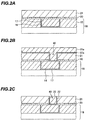
- Fig. 1 is a cross sectional view of a semiconductor device according to the embodiment.
- an element isolation insulating film 2 of a shallow trench isolation (STI) structure is formed to define active regions.
- a MOS transistor 3 is formed in an active region.
- the MOS transistor 3 is constituted of a source region 3S, a drain region 3D, a gate insulating film 31 and a gate electrode 3G.
- An interlayer insulating film 10 of silicon oxide having a thickness of 300 nm and a protective film 11 of silicon carbide (SiC) having a thickness of 50 nm are formed on the semiconductor substrate 1, covering the MOS transistor 3.
- a via hole is formed through the protective film 11 and interlayer insulating film 10, exposing a partial surface of the drain region 3D on the bottom of the via hole.
- a conductive plug 13 of tungsten (W) is filled in the via hole.
- a barrier metal layer 12 of TiN having a thickness of 25 nm is disposed between the conductive plug 13 and the inner surface of the via hole.
- An interlayer insulating film 15 of porous silica having a thickness of 150 nm is formed on the protective film 11.
- a wiring groove is formed through the interlayer insulating film 15, passing over the underlying conductive plug 13.
- a wiring 17 of copper is filled.
- a barrier metal layer 16 of tantalum (Ta) having a thickness of 15 nm is formed between the wiring 17 and the inner surface of the wiring trench.
- a cap film 20 of SiC having a thickness of 80 nm and an interlayer insulating film 21 of porous silica having a thickness of 300 nm are formed on the interlayer insulating film 15.
- a via hole is formed through the two films 21 and 20, exposing a partial upper surface of the underlying wiring 17 on the bottom of the via hole.
- a diameter of the via hole is, for example, 130 nm.
- a conductive plug 23 of Cu is filled in the via hole.
- a barrier metal layer 22 of Ta having a thickness of 15 nm is disposed between the conductive plug 23 and the inner surface of the via hole.
- the cap film 20 prevents diffusion of Cu atoms in the underlying Cu wiring 17.
- a cap film 25 of SiC having a thickness of 50 nm and an interlayer insulating film 26 of porous silica having a thickness of 150 nm are formed on the interlayer insulating film 21.
- a wiring groove is formed through the two films 26 and 25, passing over the underlying conductive plug 23.
- a width of the wiring groove is, for example, 130 nm.
- a wiring 28 of Cu is filled in this wiring groove.
- a barrier metal layer 27 of Ta having a thickness of 15 nm is disposed between the wiring 28 and the inner surface of the wiring groove. The barrier metal layer 27 is also disposed between the wiring 28 and conductive plug 23.
- a cap film 30 of SiC having a thickness of 50 nm and an interlayer insulating film 31 of porous silica having a thickness of 550 nm are formed on the interlayer insulating film 26.
- a Cu wiring 33 is filled in the cap film 30 and interlayer insulating film 31 by a dual damascene method.
- a barrier metal layer 32 of Ta having a thickness of 15 nm is disposed between the Cu wiring 33 and the via hole and wiring groove.
- the element isolation insulating film 2, MOS transistor 3, interlayer insulating film 10, protective film 11, barrier metal layer 12 and conductive plug 13 shown in Fig. 1 can be formed well-known photolithography, etching, chemical vapor deposition (CVD), chemical mechanical polishing (CMP) and the like.
- the interlayer insulating film 15 of porous silica is formed on the protective film 11.
- the interlayer insulating film 15 can be formed by coating Nano Clustering Silica (NCS) which is low dielectric constant material available from Catalysts & Chemicals Ind. Co. Ltd.
- NCS Nano Clustering Silica
- the wiring groove is formed through the interlayer insulating film 15. The upper surface of the underlying conductive plug 13 is therefore exposed on the bottom of the wiring groove.
- a Ta film is formed by sputtering, the Ta film covering the inner surface of the wiring groove and the upper surface of the interlayer insulating film 15.
- a Cu seed layer is formed on the Ta film by sputtering. On the seed layer, Cu is deposited by electrolytic plating to fill Cu in the wiring groove.
- the Ta film and Cu film deposited at a level higher than the upper surface of the interlayer insulating film 15 are removed by CMP to thereby leave the barrier metal layer 16 and Cu wiring 17 in the wiring groove.
- an underlying substrate 18 can be obtained which exposes the upper surface of the Cu wiring 17 on a partial surface of the substrate.
- the cap film 20 of SiC is formed by CVD.
- the interlayer insulating film 21 of porous silica is formed on the cap film 20, the interlayer insulating film 21 of porous silica is formed.
- the interlayer insulating film 21 can be formed by the same method as that used for forming the lower level interlayer insulating film 15.
- a via hole 40 is formed through the interlayer insulating film 21 and cap layer 20, exposing a partial surface of the underlying wiring 17.
- dry etching is performed by using total F-series substitution fluorocarbon as etching gas.
- cap layer 20 of SiC dry etching is performed by using H-containing fluorocarbon as etching gas.
- a Ta film 22a is formed by sputtering, covering the inner surface of the via hole 40 and the upper surface of the interlayer insulating film 21.
- a Cu seed layer is formed by sputtering.
- Cu is deposited through electrolytic plating by using via hole filling solution to form a Cu film 23a.
- the Cu film 23a deposited has a thickness sufficient for completely filling the via hole 40 with the Cu film 23a.
- the Ta film 22a and Cu film 23a deposited at a level higher than the upper surface of the interlayer insulating film 21 are removed by CMP.
- the barrier metal layer 22 of Ta and the Cu wiring 23 are therefore left in the via hole 40.
- the cap film 25 of SiC and the interlayer insulating film 26 of porous silica are formed by the same method as that used for forming the lower level cap film 20 and interlayer insulating film 21.
- a wiring groove 41 is formed through the interlayer insulating film 26 and cap film 25, exposing the upper surface of the conductive plug 23 on the bottom of the wiring groove 41.
- a Ta film 27a is formed by sputtering, covering the inner surface of the wiring groove 41 and the upper surface of the interlayer insulating film 26.
- a Cu seed layer is formed by sputtering.
- Cu is deposited through electrolytic plating by using wiring depositing solution to form a Cu film 28a.
- the Cu film 28a deposited has a thickness sufficient for completely filling the wiring groove 41 with the Cu film 28a.
- the Cu film 28a and Ta film 27a are subjected to CMP to expose the upper surface of the interlayer insulating film 26.
- the barrier metal layer 27 of Ta and the Cu wiring 28 are therefore left in the wiring groove 41.
- a via layer including the interlayer insulating film 21 and conductive plug 23 and a wiring layer including the interlayer insulating film 26 and wiring 28 are formed by a single damascene method.
- a wiring layer including the cap film 30, interlayer insulating film 31, barrier metal layer 32 and Cu wiring 33 shown in Fig. 1 is formed by a dual damascene method.
- Electrolytic plating solution for the Cu wiring 33 may be the via hole filling solution used for forming the lower level conductive plug 33 of the wiring depositing solution used for forming the lower level wiring 28.
- the via hole filling solution used in this embodiment is manufactured by Rohm and Haas Company of USA and contains 5 to 10 ml/l of accelerator for increasing a film forming speed, 1 to 5 ml/l of suppressor for decreasing the film forming speed, and 1 to 3 ml/l of leveler for smoothing a film surface.
- the wiring depositing solution is manufactured by Enthone Inc. and contains 5 to 10 ml/l of accelerator, 1 to 5 ml/l of suppressor and 1 to 3 ml/l of leveler.
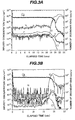
- Figs. 3A and 3B are graphs showing the measurement results, by secondary ion mass spectroscopy (SIMS), of impurity concentrations of a Cu film formed by using via hole filling solution and a Cu film formed by using wiring depositing solution, respectively.
- the abscissa represents a lapsed time from the analysis start in the unit of "minute” and the left ordinate represents an impurity concentration in the unit of "atoms/cm3".
- the right ordinate represents the number of detected secondary ions in the unit of ions/s”.
- the abscissa corresponds to the position of the Cu film in the depth direction.
- Polygonal lines fixed with symbols Cu, N, C, O, S and Cl represent the impurity concentrations of copper, nitrogen, carbon, oxygen, sulfur and chlorine, respectively.
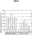
- Fig. 4 shows the concentrations of impurity elements averaged relative to the depth direction of the Cu film.
- Five left bar graphs represent the impurity concentrations of the Cu film formed by using the wiring depositing solution, and five right bar graphs represent the impurity concentrations of the Cu film formed by using the via hole filling solution. It can be seen that the impurity concentrations of the Cu film formed by using the wiring depositing solution are higher than the impurity concentrations of the Cu film formed by using the via hole filling solution. In other words, the purity of Cu of the Cu film formed by using the wiring depositing solution is lower than the purity of Cu of the Cu film formed by using the via hole filling solution.
- the total impurity concentration of carbon, oxygen, nitrogen, sulfur and chlorine of the Cu film formed by using the wiring depositing solution is about 1 x 10 20 atoms/cm 3
- the total impurity concentration of the Cu film formed by using the via hole filling solution is about 1 x 10 18 atoms/cm.
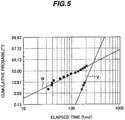
- Fig. 5 shows the results of reliability evaluation tests of evaluation samples each having a plurality of conductive plugs and wirings connected in series.
- the abscissa represents an elapsed time (in hours) from when a predetermined current is passed through each evaluation sample, and the ordinate represents a cumulative probability of failure occurrence.
- Two groups of samples were prepared: a group W of evaluation samples whose conductive plugs and wires were formed by using the wiring depositing solution, and a group V of evaluation samples whose conductive plugs were formed by the via hole filling solution and whose wirings were formed by using the wiring depositing solution. Namely, the impurity concentration of the conductive plug of the group V sample is lower than that of the wiring.
- Twenty samples were evaluated for each of the groups W and V. In Fig. 5 , straight lines W and V indicate the measurement results of the evaluation samples of the groups W and V, respectively.
- the electromigration resistance and maximum allowable current density can be improved by setting the impurity concentration of Cu of the conductive plug lower than the impurity concentration of Cu of the wiring. Improvement in the electromigration resistance may be ascribed to the fact that voids are less liable to be formed in the conductive plug because the impurity concentration of the conductive plug is set lower.
- the impurity concentration of C of the conductive plug is set relatively low, whereas the impurity concentration of C of the wiring is set relatively high. Since the volume of the conductive plug is smaller than that of the wiring, the conductive plug is less influenced by degradation of the stressmigration resistance. Therefore, as shown in Fig. 5 , a sufficient stressmigration is ensured while the high electromigration resistance is retained.
- the total atom concentration of carbon, oxygen, nitrogen, sulfur and chlorine of the conductive plug is set to equal to or lower than one tenth of the total atom concentration of the wiring. It is also preferable that the total atom concentration of the conductive plug is set lower than 1 x 10 19 cm -3 and the total atom concentration of the wiring is set higher than 1 x 10 19 cm -3 .
- the wiring 33 may be formed by using either the via hole filling solution or the wiring depositing solution. Since the higher level wiring has a larger size (width) than that of a lower level wiring, the upper level wiring is intrinsically dispensed with (i.e. does not suffer from) the problem associated with electromigration and stressmigration.
- the wiring and conductive plug are made of Cu, similar advantages are expected even if they are made of alloy mainly consisting expected even if they are made of alloy mainly consisting of Cu.
- the impurity atom concentration of the electrolytic plating solution for forming the conductive plug is set lower than that of the electrolytic plating solution for forming the wiring, to set the impurity concentration of the conductive plug lower than that of the wiring.
- the impurity concentration of plated copper can be adjusted by changing the electrolytic plating current by using the same electrolytic plating solution.
Landscapes
- Internal Circuitry In Semiconductor Integrated Circuit Devices (AREA)
- Electrodes Of Semiconductors (AREA)
Claims (4)
- Halbleitervorrichtung, umfassend:ein unterliegendes Substrat;eine erste Zwischen-/Isolierschicht, die über dem unterliegenden Substrat ausgebildet und aus Isoliermaterial hergestellt ist;ein Durchkontaktierungsloch, das durch die erste Zwischen-/Isolierschicht hindurch ausgebildet ist;einen leitfähigen Stopfen, der in das Durchkontaktierungsloch gefüllt und aus Kupfer oder einer Legierung, die hauptsächlich aus Kupfer besteht, hergestellt ist;eine zweite Zwischen-/Isolierschicht, die über der ersten Zwischen-/Isolierschicht ausgebildet und aus Isoliermaterial hergestellt ist;eine Verdrahtungsnut, die in der zweiten Zwischen-/Isolierschicht ausgebildet ist und über den leitfähigen Stopfen verläuft und eine obere Fläche des leitfähigen Stopfens freilegt; undeine Verdrahtung, die in die Verdrahtungsnut gefüllt und aus Kupfer oder einer Legierung, die hauptsächlich aus Kupfer besteht, hergestellt ist, wobeieine Gesamtatomkonzentration von Kohlenstoff, Sauerstoff, Stickstoff, Schwefel und Chlor in dem leitfähigen Stopfen niedriger ist als eine Gesamtatomkonzentration von Kohlenstoff, Sauerstoff, Stickstoff, Schwefel und Chlor in der Verdrahtung,dadurch gekennzeichnet, dassdie Gesamtatomkonzentration von Kohlenstoff, Sauerstoff, Stickstoff, Schwefel und Chlor in dem leitfähigen Stopfen gleich oder niedriger als ein(em) Zehntel der Gesamtatomkonzentration von Kohlenstoff, Sauerstoff, Stickstoff, Schwefel und Chlor in der Verdrahtung ist.
- Halbleitervorrichtung nach Anspruch 1, wobei zwischen einer Innenfläche der Verdrahtungsnut und der Verdrahtung eine Barrieremetallschicht zum Verhindern einer Kupferdiffusion angeordnet ist und die Barrieremetallschicht auch zwischen der Verdrahtung und dem leitfähigen Stopfen angeordnet ist.
- Halbleitervorrichtung nach einem der Ansprüche 1 und 2, wobei die Gesamtatomkonzentration von Kohlenstoff, Sauerstoff, Stickstoff, Schwefel und Chlor in dem leitfähigen Stopfen niedriger als 1 x 1019cm-3 ist und die Gesamtatomkonzentration von Kohlenstoff, Sauerstoff, Stickstoff, Schwefel und Chlor in der Verdrahtung höher als 1 x 1019cm-3 ist.
- Halbleiterherstellungsverfahren, das folgende Schritte umfasst:(a) Ausbilden einer ersten Zwischen-/Isolierschicht, die aus Isoliermaterial hergestellt ist, über einem unterliegenden Substrat;(b) Ausbilden eines Durchkontaktierungslochs durch die erste Zwischen-/Isolierschicht hindurch;(c) Füllen eines leitfähigen Stopfens, der aus Kupfer oder einer Legierung, die hauptsächlich aus Kupfer besteht, hergestellt ist, in das Durchkontaktierungsloch mittels eines Beschichtungsverfahrens;(d) Ausbilden einer zweiten Zwischen-/Isolierschicht, die aus Isoliermaterial hergestellt ist, über der ersten Zwischen-/Isolierschicht mit dem eingefüllten leitfähigen Stopfen;(e) Ausbilden einer Verdrahtungsnut in der zweiten Zwischen-/Isolierschicht, wobei die Verdrahtungsnut eine obere Fläche des leitfähigen Stopfens freilegt; und(f) Füllen einer Verdrahtung, die aus Kupfer oder einer Legierung, die hauptsächlich aus Kupfer besteht, hergestellt ist, in die Verdrahtungsnut mittels eines Beschichtungsverfahrens, das ein Beschichtungsbad benutzt, das anders ist als das Beschichtungsbad, das bei Schritt (c) zu verwenden ist, wobeieine Gesamtatomkonzentration von Kohlenstoff, Sauerstoff, Stickstoff, Schwefel und Chlor in dem Beschichtungsbad, das bei Schritt (f) benutzt wird, höher ist als eine Gesamtatomkonzentration von Kohlenstoff, Sauerstoff, Stickstoff, Schwefel und Chlor, die bei Schritt (c) benutzt wird.
Applications Claiming Priority (1)
| Application Number | Priority Date | Filing Date | Title |
|---|---|---|---|
| JP2004207251A JP4178295B2 (ja) | 2004-07-14 | 2004-07-14 | 銅からなる配線を有する半導体装置及びその製造方法 |
Publications (3)
| Publication Number | Publication Date |
|---|---|
| EP1617469A2 EP1617469A2 (de) | 2006-01-18 |
| EP1617469A3 EP1617469A3 (de) | 2011-03-16 |
| EP1617469B1 true EP1617469B1 (de) | 2019-04-17 |
Family
ID=35106911
Family Applications (1)
| Application Number | Title | Priority Date | Filing Date |
|---|---|---|---|
| EP05254190.1A Expired - Lifetime EP1617469B1 (de) | 2004-07-14 | 2005-07-04 | Halbleitervorrichtung mit Kupferverdrahtung, und Verfahren zu deren Herstellung |
Country Status (6)
| Country | Link |
|---|---|
| US (2) | US7205667B2 (de) |
| EP (1) | EP1617469B1 (de) |
| JP (1) | JP4178295B2 (de) |
| KR (1) | KR100662071B1 (de) |
| CN (1) | CN100420008C (de) |
| TW (1) | TWI302347B (de) |
Families Citing this family (16)
| Publication number | Priority date | Publication date | Assignee | Title |
|---|---|---|---|---|
| US7345343B2 (en) * | 2005-08-02 | 2008-03-18 | Texas Instruments Incorporated | Integrated circuit having a top side wafer contact and a method of manufacture therefor |
| JP4589835B2 (ja) * | 2005-07-13 | 2010-12-01 | 富士通セミコンダクター株式会社 | 半導体装置の製造方法及び半導体装置 |
| JP4485466B2 (ja) * | 2005-12-27 | 2010-06-23 | 株式会社神戸製鋼所 | 半導体装置の配線用金属薄膜及び半導体装置用配線 |
| JP4676350B2 (ja) * | 2006-02-14 | 2011-04-27 | ルネサスエレクトロニクス株式会社 | 半導体装置およびその製造方法 |
| US20070257323A1 (en) * | 2006-05-05 | 2007-11-08 | Taiwan Semiconductor Manufacturing Co., Ltd. | Stacked contact structure and method of fabricating the same |
| WO2008084524A1 (ja) | 2007-01-09 | 2008-07-17 | Fujitsu Microelectronics Limited | 半導体装置の製造方法、および半導体装置の製造装置 |
| JP5333207B2 (ja) * | 2007-03-05 | 2013-11-06 | 富士通セミコンダクター株式会社 | 拡散係数の算定方法 |
| US8030733B1 (en) | 2007-05-22 | 2011-10-04 | National Semiconductor Corporation | Copper-compatible fuse target |
| US7964934B1 (en) | 2007-05-22 | 2011-06-21 | National Semiconductor Corporation | Fuse target and method of forming the fuse target in a copper process flow |
| JP5180598B2 (ja) * | 2008-01-21 | 2013-04-10 | ルネサスエレクトロニクス株式会社 | 半導体装置およびその製造方法 |
| CN102067293B (zh) * | 2008-06-18 | 2013-07-03 | 富士通株式会社 | 半导体器件及其制造方法 |
| US7709956B2 (en) * | 2008-09-15 | 2010-05-04 | National Semiconductor Corporation | Copper-topped interconnect structure that has thin and thick copper traces and method of forming the copper-topped interconnect structure |
| US8237288B1 (en) | 2011-02-09 | 2012-08-07 | International Business Machines Corporation | Enhanced electromigration resistance in TSV structure and design |
| JP5857615B2 (ja) * | 2011-10-17 | 2016-02-10 | 富士通株式会社 | 電子装置およびその製造方法 |
| US8765602B2 (en) | 2012-08-30 | 2014-07-01 | International Business Machines Corporation | Doping of copper wiring structures in back end of line processing |
| US9685370B2 (en) * | 2014-12-18 | 2017-06-20 | Globalfoundries Inc. | Titanium tungsten liner used with copper interconnects |
Family Cites Families (17)
| Publication number | Priority date | Publication date | Assignee | Title |
|---|---|---|---|---|
| EP0751567B1 (de) * | 1995-06-27 | 2007-11-28 | International Business Machines Corporation | Kupferlegierungen für Chipverbindungen und Herstellungsverfahren |
| US6268291B1 (en) * | 1995-12-29 | 2001-07-31 | International Business Machines Corporation | Method for forming electromigration-resistant structures by doping |
| JP3526376B2 (ja) * | 1996-08-21 | 2004-05-10 | 株式会社東芝 | 半導体装置及びその製造方法 |
| US6123825A (en) * | 1998-12-02 | 2000-09-26 | International Business Machines Corporation | Electromigration-resistant copper microstructure and process of making |
| KR100385042B1 (ko) * | 1998-12-03 | 2003-06-18 | 인터내셔널 비지네스 머신즈 코포레이션 | 내 일렉트로 마이그레이션의 구조물을 도핑으로 형성하는 방법 |
| JP2000173949A (ja) | 1998-12-09 | 2000-06-23 | Fujitsu Ltd | 半導体装置及びその製造方法並びにめっき方法及び装置 |
| KR100443628B1 (ko) * | 1999-03-19 | 2004-08-09 | 동경 엘렉트론 주식회사 | 반도체 장치 및 그 제조 방법 |
| JP2001089896A (ja) * | 1999-09-20 | 2001-04-03 | Hitachi Ltd | めっき方法,めっき液,半導体装置及びその製造方法 |
| US6525425B1 (en) * | 2000-06-14 | 2003-02-25 | Advanced Micro Devices, Inc. | Copper interconnects with improved electromigration resistance and low resistivity |
| TWI238459B (en) * | 2000-11-15 | 2005-08-21 | Intel Corp | Copper alloy interconnections for integrated circuits and methods of making same |
| US6740221B2 (en) * | 2001-03-15 | 2004-05-25 | Applied Materials Inc. | Method of forming copper interconnects |
| US6500749B1 (en) * | 2001-03-19 | 2002-12-31 | Taiwan Semiconductor Manufacturing Company | Method to improve copper via electromigration (EM) resistance |
| JP4052868B2 (ja) * | 2002-04-26 | 2008-02-27 | Necエレクトロニクス株式会社 | 半導体装置の製造方法 |
| US7074709B2 (en) | 2002-06-28 | 2006-07-11 | Texas Instruments Incorporated | Localized doping and/or alloying of metallization for increased interconnect performance |
| JP2004039916A (ja) | 2002-07-04 | 2004-02-05 | Nec Electronics Corp | 半導体装置およびその製造方法 |
| US6841458B2 (en) * | 2002-09-12 | 2005-01-11 | Intel Corporation | Dopant interface formation |
| US20040155349A1 (en) * | 2003-01-07 | 2004-08-12 | Naofumi Nakamura | Semiconductor device and method of fabricating the same |
-
2004
- 2004-07-14 JP JP2004207251A patent/JP4178295B2/ja not_active Expired - Fee Related
- 2004-11-23 US US10/995,082 patent/US7205667B2/en not_active Expired - Lifetime
-
2005
- 2005-06-14 TW TW094119613A patent/TWI302347B/zh not_active IP Right Cessation
- 2005-06-16 KR KR1020050051727A patent/KR100662071B1/ko not_active Expired - Fee Related
- 2005-07-01 CN CNB2005100822399A patent/CN100420008C/zh not_active Expired - Lifetime
- 2005-07-04 EP EP05254190.1A patent/EP1617469B1/de not_active Expired - Lifetime
-
2007
- 2007-03-07 US US11/714,886 patent/US7871924B2/en active Active
Non-Patent Citations (1)
| Title |
|---|
| None * |
Also Published As
| Publication number | Publication date |
|---|---|
| US20060012046A1 (en) | 2006-01-19 |
| TW200605202A (en) | 2006-02-01 |
| CN1722428A (zh) | 2006-01-18 |
| KR100662071B1 (ko) | 2006-12-27 |
| EP1617469A2 (de) | 2006-01-18 |
| CN100420008C (zh) | 2008-09-17 |
| EP1617469A3 (de) | 2011-03-16 |
| KR20060046461A (ko) | 2006-05-17 |
| US20070161242A1 (en) | 2007-07-12 |
| JP4178295B2 (ja) | 2008-11-12 |
| US7871924B2 (en) | 2011-01-18 |
| TWI302347B (en) | 2008-10-21 |
| JP2006032545A (ja) | 2006-02-02 |
| US7205667B2 (en) | 2007-04-17 |
Similar Documents
| Publication | Publication Date | Title |
|---|---|---|
| US7871924B2 (en) | Semiconductor device having copper wiring | |
| US8383509B2 (en) | Manufacture method for semiconductor device having improved copper diffusion preventive function of plugs and wirings made of copper or copper alloy and semiconductor device of this kind | |
| US10332838B2 (en) | Schemes for forming barrier layers for copper in interconnect structures | |
| US7074709B2 (en) | Localized doping and/or alloying of metallization for increased interconnect performance | |
| US8853074B2 (en) | Method of manufacturing semiconductor device | |
| US7800229B2 (en) | Semiconductor device and method for manufacturing same | |
| JP2005158930A (ja) | 半導体装置およびその製造方法 | |
| US6150268A (en) | Barrier materials for metal interconnect | |
| US10211279B2 (en) | Tunable resistor with curved resistor elements | |
| US7169706B2 (en) | Method of using an adhesion precursor layer for chemical vapor deposition (CVD) copper deposition |
Legal Events
| Date | Code | Title | Description |
|---|---|---|---|
| PUAI | Public reference made under article 153(3) epc to a published international application that has entered the european phase |
Free format text: ORIGINAL CODE: 0009012 |
|
| AK | Designated contracting states |
Kind code of ref document: A2 Designated state(s): AT BE BG CH CY CZ DE DK EE ES FI FR GB GR HU IE IS IT LI LT LU LV MC NL PL PT RO SE SI SK TR |
|
| AX | Request for extension of the european patent |
Extension state: AL BA HR MK YU |
|
| RAP1 | Party data changed (applicant data changed or rights of an application transferred) |
Owner name: FUJITSU MICROELECTRONICS LIMITED |
|
| RAP1 | Party data changed (applicant data changed or rights of an application transferred) |
Owner name: FUJITSU SEMICONDUCTOR LIMITED |
|
| PUAL | Search report despatched |
Free format text: ORIGINAL CODE: 0009013 |
|
| AK | Designated contracting states |
Kind code of ref document: A3 Designated state(s): AT BE BG CH CY CZ DE DK EE ES FI FR GB GR HU IE IS IT LI LT LU LV MC NL PL PT RO SE SI SK TR |
|
| AX | Request for extension of the european patent |
Extension state: AL BA HR MK YU |
|
| RIC1 | Information provided on ipc code assigned before grant |
Ipc: H01L 23/532 20060101ALI20110204BHEP Ipc: H01L 21/288 20060101ALI20110204BHEP Ipc: H01L 21/768 20060101AFI20051027BHEP |
|
| 17P | Request for examination filed |
Effective date: 20110907 |
|
| AKX | Designation fees paid |
Designated state(s): DE |
|
| 17Q | First examination report despatched |
Effective date: 20140829 |
|
| RAP1 | Party data changed (applicant data changed or rights of an application transferred) |
Owner name: FUJITSU SEMICONDUCTOR LIMITED |
|
| STAA | Information on the status of an ep patent application or granted ep patent |
Free format text: STATUS: EXAMINATION IS IN PROGRESS |
|
| GRAP | Despatch of communication of intention to grant a patent |
Free format text: ORIGINAL CODE: EPIDOSNIGR1 |
|
| STAA | Information on the status of an ep patent application or granted ep patent |
Free format text: STATUS: GRANT OF PATENT IS INTENDED |
|
| INTG | Intention to grant announced |
Effective date: 20181107 |
|
| GRAS | Grant fee paid |
Free format text: ORIGINAL CODE: EPIDOSNIGR3 |
|
| GRAA | (expected) grant |
Free format text: ORIGINAL CODE: 0009210 |
|
| STAA | Information on the status of an ep patent application or granted ep patent |
Free format text: STATUS: THE PATENT HAS BEEN GRANTED |
|
| REG | Reference to a national code |
Ref country code: DE Ref legal event code: R081 Ref document number: 602005055660 Country of ref document: DE Owner name: FUJITSU SEMICONDUCTOR LIMITED, YOKOHAMA-SHI, JP Free format text: FORMER OWNER: FUJITSU LIMITED, KAWASAKI-SHI, KANAGAWA, JP |
|
| AK | Designated contracting states |
Kind code of ref document: B1 Designated state(s): DE |
|
| REG | Reference to a national code |
Ref country code: DE Ref legal event code: R096 Ref document number: 602005055660 Country of ref document: DE |
|
| REG | Reference to a national code |
Ref country code: DE Ref legal event code: R097 Ref document number: 602005055660 Country of ref document: DE |
|
| PLBE | No opposition filed within time limit |
Free format text: ORIGINAL CODE: 0009261 |
|
| STAA | Information on the status of an ep patent application or granted ep patent |
Free format text: STATUS: NO OPPOSITION FILED WITHIN TIME LIMIT |
|
| 26N | No opposition filed |
Effective date: 20200120 |
|
| REG | Reference to a national code |
Ref country code: DE Ref legal event code: R082 Ref document number: 602005055660 Country of ref document: DE Representative=s name: HASELTINE LAKE KEMPNER LLP, DE Ref country code: DE Ref legal event code: R081 Ref document number: 602005055660 Country of ref document: DE Owner name: FUJITSU SEMICONDUCTOR LIMITED, YOKOHAMA-SHI, JP Free format text: FORMER OWNER: FUJITSU SEMICONDUCTOR LIMITED, YOKOHAMA-SHI, KANAGAWA, JP Ref country code: DE Ref legal event code: R082 Ref document number: 602005055660 Country of ref document: DE Representative=s name: HL KEMPNER PATENTANWALT, RECHTSANWALT, SOLICIT, DE |
|
| PGFP | Annual fee paid to national office [announced via postgrant information from national office to epo] |
Ref country code: DE Payment date: 20200624 Year of fee payment: 16 |
|
| REG | Reference to a national code |
Ref country code: DE Ref legal event code: R082 Ref document number: 602005055660 Country of ref document: DE Representative=s name: HL KEMPNER PATENTANWALT, RECHTSANWALT, SOLICIT, DE |
|
| REG | Reference to a national code |
Ref country code: DE Ref legal event code: R119 Ref document number: 602005055660 Country of ref document: DE |
|
| PG25 | Lapsed in a contracting state [announced via postgrant information from national office to epo] |
Ref country code: DE Free format text: LAPSE BECAUSE OF NON-PAYMENT OF DUE FEES Effective date: 20220201 |