EP1595284B1 - Elektrostatische bond-einspannvorrichtung mit integrierter hochfrequenzelektrode und thermostatischen mitteln - Google Patents
Elektrostatische bond-einspannvorrichtung mit integrierter hochfrequenzelektrode und thermostatischen mitteln Download PDFInfo
- Publication number
- EP1595284B1 EP1595284B1 EP04708363A EP04708363A EP1595284B1 EP 1595284 B1 EP1595284 B1 EP 1595284B1 EP 04708363 A EP04708363 A EP 04708363A EP 04708363 A EP04708363 A EP 04708363A EP 1595284 B1 EP1595284 B1 EP 1595284B1
- Authority
- EP
- European Patent Office
- Prior art keywords
- pedestal
- chuck according
- ceramic part
- bottom ceramic
- ceramic
- Prior art date
- Legal status (The legal status is an assumption and is not a legal conclusion. Google has not performed a legal analysis and makes no representation as to the accuracy of the status listed.)
- Expired - Lifetime
Links
Images
Classifications
-
- H10P72/72—
-
- H10P72/0432—
Definitions
- the present invention relates to an electrostatic holding soleplate with radiofrequency electrode and integrated thermostatic means. It applies, in particular but not exclusively, to the manufacture of electronic components.
- PVD Physical Vapor Deposition
- MOS transistors Metal Oxid Semiconductors for metal oxide semiconductors
- PVD Physical Vapor Deposition
- the copper deposition is carried out mainly by an electrodeposition reaction in a liquid medium which previously requires the deposition of a copper seed layer by PVD.
- This germinal layer has extremely critical characteristics.
- the present invention by its specific properties, participates in obtaining these characteristics.
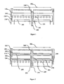
- Figure 1 shows a sole (in English "chuck") according to the prior art.
- a substrate 100 for example a silicon wafer
- the soleplate 110 rests, on the other hand even, on a support 140 (or pedestal) having cooling circuits 150, heating resistors 160.
- the sole has a central opening 180, in the axis of the central opening 120 of the sole 110. By these openings is injected with a gas 190, for example helium or argon, promoting the heat exchange between the support 140, the soleplate 110 and the substrate 100.
- a gas 190 for example helium or argon
- the present invention aims to remedy these disadvantages.
- Radiofrequency electrodes are used to modulate the plasma around the substrate to be treated.
- the ceramics are glued together by heated glass. Thanks to these arrangements, the bonding is insulating and very resistant and it is possible to reduce the stresses and provisions relating to the insulation of the RF electrodes, since the pedestal can be grounded.
- the electrostatic sole comprises a pedestal carrying cooling elements, the lower ceramic being assembled to the pedestal in a durable manner.
- the lower ceramic is assembled to the pedestal by soldered connection.
- the brazing of the soldered connection is indium.
- the lower ceramic is assembled to the pedestal by gluing.
- the collage is silver.
- the lower ceramic and the pedestal are in good thermal connection and the RF electrodes are isolated from the pedestal.
- the lower ceramic has cooling elements.
- the lower ceramic is carried by lateral supports durably assembled to said lower ceramic.
- FIG. 2 shows an electrostatic plate 250 (in English "chuck") according to one embodiment of the present invention.
- a substrate 200 in English "wafer" which is based on an upper ceramic 205 of the electrostatic sole 250, provided with a central opening gas inlet 210.
- the upper ceramic 205 is glued by an adhesive 260 , to a lower ceramic 215 which carries radio frequency electrodes RF 220 and heating elements 225.
- the lower ceramic 215 is itself permanently assembled to a support 230 (or pedestal) having cooling circuits 235.
- the ceramic bottom 215 has a central gas inlet opening 240, in the axis of the central gas inlet opening 210 of the upper ceramic 205.
- the pedestal 230 has a central gas inlet opening 245, axis of the central gas inlet openings 210 and 240 of the upper and lower ceramics.
- a gas 255 for example helium or argon, promoting heat exchange between the upper ceramic 205 and the substrate 200.
- the adhesive 260 is, in a particularly advantageous embodiment, a glue made of glass which is applied at a temperature at which the glass is liquid and malleable. Bonding thus provides electrical insulation between the two ceramics.
- the RF radiofrequency electrodes 220 are, for example, flat electrodes positioned on the upper face of the lower ceramic 215.
- the heating elements 225 are, for example, flat electrodes positioned on the lower face of the lower ceramic 215.
- the assembly between the lower ceramic 215 and the pedestal 230 is, for example formed by brazed connection using an indium solder 270 ensuring a good thermal bond.
- the assembly between the lower ceramic 215 and the pedestal 230 is formed by gluing, for example with a silver glue 270.
- the pins 265 allow handling slices.
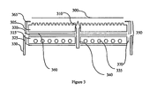
- FIG. 3 shows an electrostatic plate 350 (in English "chuck") according to one embodiment of the present invention.
- a substrate 300 in English "wafer" which is based on an upper ceramic 305 of the electrostatic sole 350, provided with a central opening gas inlet 310.
- the upper ceramic 305 is glued, by a glue 360 , to a lower ceramic 315 which carries RF radiofrequency electrodes 320, heating elements 325 and cooling circuits 335.
- the lower ceramic 315 is itself, durably assembled, by its lateral faces, to a support 330.
- the lower ceramic 315 has a central gas inlet opening 340, in the axis of the central gas inlet opening 310 of the upper ceramic 305.
- a gas 350 for example helium or argon, promoting the heat exchange between the upper ceramic 305 and the substrate 300.
- the adhesive 360 is, in a particularly advantageous embodiment, a glue made of glass which is applied at a temperature at which the glass is liquid and malleable. Bonding thus provides electrical insulation between the two ceramics.
- the RF radiofrequency electrodes 320 are, for example, flat electrodes positioned on the upper face of the lower ceramic 315.
- the heating elements 325 are, for example, flat electrodes positioned on the lower face of the lower ceramic 315.
- connection between the lower ceramic 315 and the support 330 is, for example formed by brazed connection using an indium solder 370 ensuring a good thermal bond.
- connection between the lower ceramic 315 and the support 330 is formed by gluing, for example with a silver glue 370.
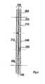
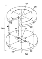
- FIG. 4 in section and in FIG. 5, in perspective, the electrostatic plate illustrated in FIG. 2 is seen.
- FIG. 5 the two ceramics 205 and 215 are separated for explanatory purposes.
- FIGS. 4 and 5 show the electrostatic sole 250 comprising the upper ceramic 205 and the lower ceramic 215, the central openings 210 and 240, the adhesive layer 260, the RF radiofrequency electrodes 220 and the heating elements 225.
- Six recesses Lateral cylindrical cylinders 400 parallel to the axis of the ceramics are formed at regular intervals on the ceramics, so that the slices handling pieces 365 are housed therein.
Landscapes
- Engineering & Computer Science (AREA)
- Container, Conveyance, Adherence, Positioning, Of Wafer (AREA)
- Computer Hardware Design (AREA)
- Condensed Matter Physics & Semiconductors (AREA)
- General Physics & Mathematics (AREA)
- Manufacturing & Machinery (AREA)
- Physics & Mathematics (AREA)
- Microelectronics & Electronic Packaging (AREA)
- Power Engineering (AREA)
- Electrotherapy Devices (AREA)
- Filters And Equalizers (AREA)
- Non-Reversible Transmitting Devices (AREA)
- Piezo-Electric Or Mechanical Vibrators, Or Delay Or Filter Circuits (AREA)
Claims (10)
- Elektrostatische Bond-Einspannvorrichtung (250, 350), dadurch gekennzeichnet, daß sie aufweist:- einen oberen Keramikkörper (205), der zum Halten des zu behandelnden Substrats (200, 300) eingerichtet ist,- einen unteren Keramikkörper (215, 315), der Heizelemente (225, 325) und Hochfrequenzelektroden (220, 320) trägt,wobei die genannten Keramikkörper miteinander dauerhaft verklebt sind.
- Bond-Einspannvorrichtung nach Anspruch 1, dadurch gekennzeichnet, daß die Keramikkörper (205, 215, 315) miteinander durch erhitztes Glas (260, 360) verklebt sind.
- Bond-Einspannvorrichtung nach einem der Ansprüche 1 oder 2, dadurch gekennzeichnet, daß sie einen Sockel (230) aufweist, der Kühlelemente (235) trägt, wobei der untere Keramikkörper (215) mit dem Sockel dauerhaft zusammengebaut ist.
- Bond-Einspannvorrichtung nach Anspruch 3, dadurch gekennzeichnet, daß der untere Keramikkörper (215, 315) mit dem Sockel (230, 330) durch eine Lötverbindung (270, 370) verbunden ist.
- Bond-Einspannvorrichtung nach Anspruch 4, dadurch gekennzeichnet, daß die Lötverbindung (270, 370) mit Indiumlot hergestellt ist.
- Bond-Einspannvorrichtung nach Anspruch 3, dadurch gekennzeichnet, daß der untere Keramikkörper (215, 315) mit dem Sockel (230, 330) durch Kleben zusammengebaut ist.
- Bond-Einspannvorrichtung nach Anspruch 6, dadurch gekennzeichnet, daß die Verklebung (270, 370) des unteren Keramikkörpers (215, 315) mit dem Sockel (230, 330) mit Silber hergestellt ist.
- Bond-Einspannvorrichtung nach einem der Ansprüche 1 bis 7, dadurch gekennzeichnet, daß der untere Keramikkörper (315) Kühlelemente (335) aufweist.
- Bond-Einspannvorrichtung nach einem der Ansprüche 1 bis 8, dadurch gekennzeichnet, daß der untere Keramikkörper (215, 315) von seitlichen Haltern getragen ist, die dauerhaft mit dem unteren Keramikkörper zusammengebaut sind.
- Bond-Einspannvorrichtung nach einem der Ansprüche 1 bis 9, dadurch gekennzeichnet, daß jeder der oberen und unteren Keramikkörper (205, 215, 315) von einer Gaseintrittsöffnung (210, 240, 245, 310, 340) durchsetzt ist.
Applications Claiming Priority (3)
| Application Number | Priority Date | Filing Date | Title |
|---|---|---|---|
| FR0301323 | 2003-02-05 | ||
| FR0301323A FR2850790B1 (fr) | 2003-02-05 | 2003-02-05 | Semelle de collage electrostatique avec electrode radiofrequence et moyens thermostatiques integres |
| PCT/EP2004/050083 WO2004070829A1 (fr) | 2003-02-05 | 2004-02-05 | Semelle de collage electrostatique avec electrode radiofrequence et moyens thermostatiques integres |
Publications (2)
| Publication Number | Publication Date |
|---|---|
| EP1595284A1 EP1595284A1 (de) | 2005-11-16 |
| EP1595284B1 true EP1595284B1 (de) | 2007-08-08 |
Family
ID=32696374
Family Applications (1)
| Application Number | Title | Priority Date | Filing Date |
|---|---|---|---|
| EP04708363A Expired - Lifetime EP1595284B1 (de) | 2003-02-05 | 2004-02-05 | Elektrostatische bond-einspannvorrichtung mit integrierter hochfrequenzelektrode und thermostatischen mitteln |
Country Status (8)
| Country | Link |
|---|---|
| US (1) | US20060164785A1 (de) |
| EP (1) | EP1595284B1 (de) |
| JP (1) | JP2006517341A (de) |
| AT (1) | ATE369625T1 (de) |
| CA (1) | CA2514616A1 (de) |
| DE (1) | DE602004008037T2 (de) |
| FR (1) | FR2850790B1 (de) |
| WO (1) | WO2004070829A1 (de) |
Families Citing this family (27)
| Publication number | Priority date | Publication date | Assignee | Title |
|---|---|---|---|---|
| USD553104S1 (en) * | 2004-04-21 | 2007-10-16 | Tokyo Electron Limited | Absorption board for an electric chuck used in semiconductor manufacture |
| USD548200S1 (en) * | 2005-09-29 | 2007-08-07 | Tokyo Electron Limited | Attracting disc for an electrostatic chuck for semiconductor production |
| USD546784S1 (en) * | 2005-09-29 | 2007-07-17 | Tokyo Electron Limited | Attracting disc for an electrostatic chuck for semiconductor production |
| TWD125773S1 (zh) * | 2006-08-01 | 2008-11-01 | 東京威力科創股份有限公司 | 半導體製造用靜電吸盤用吸附板 |
| JP5557164B2 (ja) * | 2010-03-24 | 2014-07-23 | Toto株式会社 | 静電チャック |
| US9070760B2 (en) | 2011-03-14 | 2015-06-30 | Plasma-Therm Llc | Method and apparatus for plasma dicing a semi-conductor wafer |
| US8946058B2 (en) | 2011-03-14 | 2015-02-03 | Plasma-Therm Llc | Method and apparatus for plasma dicing a semi-conductor wafer |
| US8802545B2 (en) | 2011-03-14 | 2014-08-12 | Plasma-Therm Llc | Method and apparatus for plasma dicing a semi-conductor wafer |
| US9034199B2 (en) | 2012-02-21 | 2015-05-19 | Applied Materials, Inc. | Ceramic article with reduced surface defect density and process for producing a ceramic article |
| US9212099B2 (en) | 2012-02-22 | 2015-12-15 | Applied Materials, Inc. | Heat treated ceramic substrate having ceramic coating and heat treatment for coated ceramics |
| US9090046B2 (en) | 2012-04-16 | 2015-07-28 | Applied Materials, Inc. | Ceramic coated article and process for applying ceramic coating |
| US9604249B2 (en) | 2012-07-26 | 2017-03-28 | Applied Materials, Inc. | Innovative top-coat approach for advanced device on-wafer particle performance |
| US9343289B2 (en) | 2012-07-27 | 2016-05-17 | Applied Materials, Inc. | Chemistry compatible coating material for advanced device on-wafer particle performance |
| US9916998B2 (en) | 2012-12-04 | 2018-03-13 | Applied Materials, Inc. | Substrate support assembly having a plasma resistant protective layer |
| US9685356B2 (en) * | 2012-12-11 | 2017-06-20 | Applied Materials, Inc. | Substrate support assembly having metal bonded protective layer |
| US8941969B2 (en) | 2012-12-21 | 2015-01-27 | Applied Materials, Inc. | Single-body electrostatic chuck |
| US9358702B2 (en) | 2013-01-18 | 2016-06-07 | Applied Materials, Inc. | Temperature management of aluminium nitride electrostatic chuck |
| US9669653B2 (en) | 2013-03-14 | 2017-06-06 | Applied Materials, Inc. | Electrostatic chuck refurbishment |
| US9887121B2 (en) | 2013-04-26 | 2018-02-06 | Applied Materials, Inc. | Protective cover for electrostatic chuck |
| US9666466B2 (en) | 2013-05-07 | 2017-05-30 | Applied Materials, Inc. | Electrostatic chuck having thermally isolated zones with minimal crosstalk |
| US9865434B2 (en) | 2013-06-05 | 2018-01-09 | Applied Materials, Inc. | Rare-earth oxide based erosion resistant coatings for semiconductor application |
| US9850568B2 (en) | 2013-06-20 | 2017-12-26 | Applied Materials, Inc. | Plasma erosion resistant rare-earth oxide based thin film coatings |
| KR20170026360A (ko) | 2014-06-17 | 2017-03-08 | 에바텍 아크티엔게젤샤프트 | 무선 주파수 션트를 구비한 정전척 |
| US10020218B2 (en) | 2015-11-17 | 2018-07-10 | Applied Materials, Inc. | Substrate support assembly with deposited surface features |
| US11047035B2 (en) | 2018-02-23 | 2021-06-29 | Applied Materials, Inc. | Protective yttria coating for semiconductor equipment parts |
| JP7579758B2 (ja) * | 2021-06-28 | 2024-11-08 | 東京エレクトロン株式会社 | 基板支持体、基板支持体アセンブリ及びプラズマ処理装置 |
| WO2025134325A1 (ja) * | 2023-12-21 | 2025-06-26 | 日本碍子株式会社 | 半導体製造装置用部材 |
Family Cites Families (24)
| Publication number | Priority date | Publication date | Assignee | Title |
|---|---|---|---|---|
| JP3157551B2 (ja) * | 1990-07-20 | 2001-04-16 | 東京エレクトロン株式会社 | 被処理体用載置装置及びそれを用いた処理装置 |
| EP0493089B1 (de) * | 1990-12-25 | 1998-09-16 | Ngk Insulators, Ltd. | Heizungsapparat für eine Halbleiterscheibe und Verfahren zum Herstellen desselben |
| JP3271352B2 (ja) * | 1993-01-13 | 2002-04-02 | ソニー株式会社 | 静電チャック及びその作製方法並びに基板処理装置及び基板搬送装置 |
| JPH08330402A (ja) * | 1995-03-30 | 1996-12-13 | Ngk Insulators Ltd | 半導体ウエハー保持装置 |
| JPH09172056A (ja) * | 1995-12-20 | 1997-06-30 | Souzou Kagaku:Kk | 半導体基板のプラズマ処理装置 |
| JPH09213777A (ja) * | 1996-01-31 | 1997-08-15 | Kyocera Corp | 静電チャック |
| US5754391A (en) * | 1996-05-17 | 1998-05-19 | Saphikon Inc. | Electrostatic chuck |
| JPH11354504A (ja) * | 1998-06-08 | 1999-12-24 | Sony Corp | ガラス基板処理装置 |
| US6073577A (en) * | 1998-06-30 | 2000-06-13 | Lam Research Corporation | Electrode for plasma processes and method for manufacture and use thereof |
| EP1193751B1 (de) * | 1999-04-06 | 2006-05-17 | Tokyo Electron Limited | Elektrode und herstellungsmethode für eine elektrode |
| US6490146B2 (en) * | 1999-05-07 | 2002-12-03 | Applied Materials Inc. | Electrostatic chuck bonded to base with a bond layer and method |
| US20020036881A1 (en) * | 1999-05-07 | 2002-03-28 | Shamouil Shamouilian | Electrostatic chuck having composite base and method |
| WO2001035459A1 (fr) * | 1999-11-10 | 2001-05-17 | Ibiden Co., Ltd. | Substrat en ceramique |
| JP2002057207A (ja) * | 2000-01-20 | 2002-02-22 | Sumitomo Electric Ind Ltd | 半導体製造装置用ウェハ保持体およびその製造方法ならびに半導体製造装置 |
| JP3492325B2 (ja) * | 2000-03-06 | 2004-02-03 | キヤノン株式会社 | 画像表示装置の製造方法 |
| JP2001253777A (ja) * | 2000-03-13 | 2001-09-18 | Ibiden Co Ltd | セラミック基板 |
| US6444957B1 (en) * | 2000-04-26 | 2002-09-03 | Sumitomo Osaka Cement Co., Ltd | Heating apparatus |
| TWI254403B (en) * | 2000-05-19 | 2006-05-01 | Ngk Insulators Ltd | Electrostatic clamper, and electrostatic attracting structures |
| JP2002141257A (ja) * | 2000-05-24 | 2002-05-17 | Ibiden Co Ltd | 半導体製造・検査装置用セラミックヒータ |
| JP2002016005A (ja) * | 2000-06-29 | 2002-01-18 | Sumitomo Electric Ind Ltd | 半導体製造装置用電極端子接合セラミックス部材及びその製造方法 |
| JP2002025913A (ja) * | 2000-07-04 | 2002-01-25 | Sumitomo Electric Ind Ltd | 半導体製造装置用サセプタとそれを用いた半導体製造装置 |
| US6646233B2 (en) * | 2002-03-05 | 2003-11-11 | Hitachi High-Technologies Corporation | Wafer stage for wafer processing apparatus and wafer processing method |
| US6921724B2 (en) * | 2002-04-02 | 2005-07-26 | Lam Research Corporation | Variable temperature processes for tunable electrostatic chuck |
| JP4451098B2 (ja) * | 2002-08-22 | 2010-04-14 | 住友大阪セメント株式会社 | サセプタ装置 |
-
2003
- 2003-02-05 FR FR0301323A patent/FR2850790B1/fr not_active Expired - Fee Related
-
2004
- 2004-02-05 US US10/544,516 patent/US20060164785A1/en not_active Abandoned
- 2004-02-05 WO PCT/EP2004/050083 patent/WO2004070829A1/fr not_active Ceased
- 2004-02-05 EP EP04708363A patent/EP1595284B1/de not_active Expired - Lifetime
- 2004-02-05 AT AT04708363T patent/ATE369625T1/de active
- 2004-02-05 DE DE602004008037T patent/DE602004008037T2/de not_active Expired - Lifetime
- 2004-02-05 CA CA002514616A patent/CA2514616A1/fr not_active Abandoned
- 2004-02-05 JP JP2006502004A patent/JP2006517341A/ja active Pending
Also Published As
| Publication number | Publication date |
|---|---|
| DE602004008037D1 (de) | 2007-09-20 |
| CA2514616A1 (fr) | 2004-08-19 |
| DE602004008037T2 (de) | 2008-04-30 |
| WO2004070829A1 (fr) | 2004-08-19 |
| EP1595284A1 (de) | 2005-11-16 |
| FR2850790A1 (fr) | 2004-08-06 |
| FR2850790B1 (fr) | 2005-04-08 |
| US20060164785A1 (en) | 2006-07-27 |
| ATE369625T1 (de) | 2007-08-15 |
| JP2006517341A (ja) | 2006-07-20 |
Similar Documents
| Publication | Publication Date | Title |
|---|---|---|
| EP1595284B1 (de) | Elektrostatische bond-einspannvorrichtung mit integrierter hochfrequenzelektrode und thermostatischen mitteln | |
| US10290529B2 (en) | Heater unit | |
| US5673167A (en) | Support platen with removable insert useful in semiconductor processing apparatus | |
| US20070169703A1 (en) | Advanced ceramic heater for substrate processing | |
| EP0582566A1 (de) | Keramische elektrostatische haltevorrichtung. | |
| CN103077934A (zh) | 部件的接合结构体、部件的接合方法以及封装体 | |
| JP7657780B2 (ja) | セラミックヒータおよび液相拡散接合を用いた形成方法 | |
| JP7364822B1 (ja) | ウエハ載置台 | |
| EP1239515B1 (de) | Substrat für elektronische Leistungsschaltung und elektronisches Leistungsmodul mit diesem | |
| FR2883416A1 (fr) | Dispositif a semiconducteur. | |
| JP7515017B1 (ja) | ウエハ載置台 | |
| JP7663709B2 (ja) | ウエハ載置台 | |
| CN116092904B (zh) | 晶片载放台 | |
| WO2023189954A1 (ja) | 試料保持具 | |
| CN118843929A (zh) | 试料保持工具 | |
| TWI858874B (zh) | 靜電吸盤 | |
| JP7471566B2 (ja) | 静電チャック | |
| WO2025047725A1 (ja) | 試料保持具 | |
| JP7489940B2 (ja) | 試料保持具 | |
| US20250096026A1 (en) | Substrate fixing device | |
| CN117790389A (zh) | 静电吸盘 | |
| TW201818501A (zh) | 靜電吸盤及其製作方法 |
Legal Events
| Date | Code | Title | Description |
|---|---|---|---|
| PUAI | Public reference made under article 153(3) epc to a published international application that has entered the european phase |
Free format text: ORIGINAL CODE: 0009012 |
|
| 17P | Request for examination filed |
Effective date: 20050901 |
|
| AK | Designated contracting states |
Kind code of ref document: A1 Designated state(s): AT BE BG CH CY CZ DE DK EE ES FI FR GB GR HU IE IT LI LU MC NL PT RO SE SI SK TR |
|
| AX | Request for extension of the european patent |
Extension state: AL LT LV MK |
|
| DAX | Request for extension of the european patent (deleted) | ||
| GRAP | Despatch of communication of intention to grant a patent |
Free format text: ORIGINAL CODE: EPIDOSNIGR1 |
|
| GRAS | Grant fee paid |
Free format text: ORIGINAL CODE: EPIDOSNIGR3 |
|
| GRAA | (expected) grant |
Free format text: ORIGINAL CODE: 0009210 |
|
| AK | Designated contracting states |
Kind code of ref document: B1 Designated state(s): AT BE BG CH CY CZ DE DK EE ES FI FR GB GR HU IE IT LI LU MC NL PT RO SE SI SK TR |
|
| REG | Reference to a national code |
Ref country code: GB Ref legal event code: FG4D Free format text: NOT ENGLISH |
|
| REG | Reference to a national code |
Ref country code: CH Ref legal event code: EP |
|
| REG | Reference to a national code |
Ref country code: IE Ref legal event code: FG4D Free format text: LANGUAGE OF EP DOCUMENT: FRENCH |
|
| REF | Corresponds to: |
Ref document number: 602004008037 Country of ref document: DE Date of ref document: 20070920 Kind code of ref document: P |
|
| REG | Reference to a national code |
Ref country code: SE Ref legal event code: TRGR |
|
| GBT | Gb: translation of ep patent filed (gb section 77(6)(a)/1977) |
Effective date: 20071114 |
|
| PG25 | Lapsed in a contracting state [announced via postgrant information from national office to epo] |
Ref country code: ES Free format text: LAPSE BECAUSE OF FAILURE TO SUBMIT A TRANSLATION OF THE DESCRIPTION OR TO PAY THE FEE WITHIN THE PRESCRIBED TIME-LIMIT Effective date: 20071119 Ref country code: BG Free format text: LAPSE BECAUSE OF FAILURE TO SUBMIT A TRANSLATION OF THE DESCRIPTION OR TO PAY THE FEE WITHIN THE PRESCRIBED TIME-LIMIT Effective date: 20071108 |
|
| REG | Reference to a national code |
Ref country code: CH Ref legal event code: NV Representative=s name: BOVARD AG PATENTANWAELTE |
|
| REG | Reference to a national code |
Ref country code: IE Ref legal event code: FD4D |
|
| PG25 | Lapsed in a contracting state [announced via postgrant information from national office to epo] |
Ref country code: GR Free format text: LAPSE BECAUSE OF FAILURE TO SUBMIT A TRANSLATION OF THE DESCRIPTION OR TO PAY THE FEE WITHIN THE PRESCRIBED TIME-LIMIT Effective date: 20071109 Ref country code: DK Free format text: LAPSE BECAUSE OF FAILURE TO SUBMIT A TRANSLATION OF THE DESCRIPTION OR TO PAY THE FEE WITHIN THE PRESCRIBED TIME-LIMIT Effective date: 20070808 |
|
| PG25 | Lapsed in a contracting state [announced via postgrant information from national office to epo] |
Ref country code: SK Free format text: LAPSE BECAUSE OF FAILURE TO SUBMIT A TRANSLATION OF THE DESCRIPTION OR TO PAY THE FEE WITHIN THE PRESCRIBED TIME-LIMIT Effective date: 20070808 Ref country code: PT Free format text: LAPSE BECAUSE OF FAILURE TO SUBMIT A TRANSLATION OF THE DESCRIPTION OR TO PAY THE FEE WITHIN THE PRESCRIBED TIME-LIMIT Effective date: 20080108 Ref country code: IE Free format text: LAPSE BECAUSE OF FAILURE TO SUBMIT A TRANSLATION OF THE DESCRIPTION OR TO PAY THE FEE WITHIN THE PRESCRIBED TIME-LIMIT Effective date: 20070808 |
|
| PLBE | No opposition filed within time limit |
Free format text: ORIGINAL CODE: 0009261 |
|
| STAA | Information on the status of an ep patent application or granted ep patent |
Free format text: STATUS: NO OPPOSITION FILED WITHIN TIME LIMIT |
|
| PG25 | Lapsed in a contracting state [announced via postgrant information from national office to epo] |
Ref country code: RO Free format text: LAPSE BECAUSE OF FAILURE TO SUBMIT A TRANSLATION OF THE DESCRIPTION OR TO PAY THE FEE WITHIN THE PRESCRIBED TIME-LIMIT Effective date: 20070808 |
|
| 26N | No opposition filed |
Effective date: 20080509 |
|
| BERE | Be: lapsed |
Owner name: SEMCO ENGINEERING S.A. Effective date: 20080228 |
|
| PG25 | Lapsed in a contracting state [announced via postgrant information from national office to epo] |
Ref country code: MC Free format text: LAPSE BECAUSE OF NON-PAYMENT OF DUE FEES Effective date: 20080228 |
|
| PG25 | Lapsed in a contracting state [announced via postgrant information from national office to epo] |
Ref country code: EE Free format text: LAPSE BECAUSE OF FAILURE TO SUBMIT A TRANSLATION OF THE DESCRIPTION OR TO PAY THE FEE WITHIN THE PRESCRIBED TIME-LIMIT Effective date: 20070808 |
|
| PG25 | Lapsed in a contracting state [announced via postgrant information from national office to epo] |
Ref country code: BE Free format text: LAPSE BECAUSE OF NON-PAYMENT OF DUE FEES Effective date: 20080228 |
|
| PG25 | Lapsed in a contracting state [announced via postgrant information from national office to epo] |
Ref country code: SI Free format text: LAPSE BECAUSE OF FAILURE TO SUBMIT A TRANSLATION OF THE DESCRIPTION OR TO PAY THE FEE WITHIN THE PRESCRIBED TIME-LIMIT Effective date: 20070808 |
|
| PG25 | Lapsed in a contracting state [announced via postgrant information from national office to epo] |
Ref country code: CY Free format text: LAPSE BECAUSE OF FAILURE TO SUBMIT A TRANSLATION OF THE DESCRIPTION OR TO PAY THE FEE WITHIN THE PRESCRIBED TIME-LIMIT Effective date: 20070808 |
|
| PG25 | Lapsed in a contracting state [announced via postgrant information from national office to epo] |
Ref country code: LU Free format text: LAPSE BECAUSE OF NON-PAYMENT OF DUE FEES Effective date: 20080205 Ref country code: HU Free format text: LAPSE BECAUSE OF FAILURE TO SUBMIT A TRANSLATION OF THE DESCRIPTION OR TO PAY THE FEE WITHIN THE PRESCRIBED TIME-LIMIT Effective date: 20080209 |
|
| PG25 | Lapsed in a contracting state [announced via postgrant information from national office to epo] |
Ref country code: TR Free format text: LAPSE BECAUSE OF FAILURE TO SUBMIT A TRANSLATION OF THE DESCRIPTION OR TO PAY THE FEE WITHIN THE PRESCRIBED TIME-LIMIT Effective date: 20070808 |
|
| PG25 | Lapsed in a contracting state [announced via postgrant information from national office to epo] |
Ref country code: IT Free format text: LAPSE BECAUSE OF NON-PAYMENT OF DUE FEES Effective date: 20100205 |
|
| REG | Reference to a national code |
Ref country code: CH Ref legal event code: PFA Owner name: SEMCO ENGINEERING S.A. Free format text: SEMCO ENGINEERING S.A.#625, RUE DE LA CROIX VERTE, PARC EUROMEDECINE#34196 MONTPELLIER CEDEX 5 (FR) -TRANSFER TO- SEMCO ENGINEERING S.A.#625, RUE DE LA CROIX VERTE, PARC EUROMEDECINE#34196 MONTPELLIER CEDEX 5 (FR) |
|
| PGRI | Patent reinstated in contracting state [announced from national office to epo] |
Ref country code: IT Effective date: 20110616 |
|
| PGFP | Annual fee paid to national office [announced via postgrant information from national office to epo] |
Ref country code: IT Payment date: 20120221 Year of fee payment: 9 |
|
| PGFP | Annual fee paid to national office [announced via postgrant information from national office to epo] |
Ref country code: FR Payment date: 20130228 Year of fee payment: 10 Ref country code: GB Payment date: 20130218 Year of fee payment: 10 Ref country code: CH Payment date: 20130220 Year of fee payment: 10 Ref country code: FI Payment date: 20130213 Year of fee payment: 10 Ref country code: SE Payment date: 20130219 Year of fee payment: 10 Ref country code: DE Payment date: 20130219 Year of fee payment: 10 |
|
| PGFP | Annual fee paid to national office [announced via postgrant information from national office to epo] |
Ref country code: NL Payment date: 20130219 Year of fee payment: 10 |
|
| PGFP | Annual fee paid to national office [announced via postgrant information from national office to epo] |
Ref country code: AT Payment date: 20130213 Year of fee payment: 10 |
|
| REG | Reference to a national code |
Ref country code: DE Ref legal event code: R119 Ref document number: 602004008037 Country of ref document: DE |
|
| REG | Reference to a national code |
Ref country code: NL Ref legal event code: V1 Effective date: 20140901 |
|
| REG | Reference to a national code |
Ref country code: SE Ref legal event code: EUG Ref country code: CH Ref legal event code: PL |
|
| REG | Reference to a national code |
Ref country code: AT Ref legal event code: MM01 Ref document number: 369625 Country of ref document: AT Kind code of ref document: T Effective date: 20140205 |
|
| GBPC | Gb: european patent ceased through non-payment of renewal fee |
Effective date: 20140205 |
|
| PG25 | Lapsed in a contracting state [announced via postgrant information from national office to epo] |
Ref country code: CH Free format text: LAPSE BECAUSE OF NON-PAYMENT OF DUE FEES Effective date: 20140228 Ref country code: LI Free format text: LAPSE BECAUSE OF NON-PAYMENT OF DUE FEES Effective date: 20140228 Ref country code: FI Free format text: LAPSE BECAUSE OF NON-PAYMENT OF DUE FEES Effective date: 20140205 Ref country code: NL Free format text: LAPSE BECAUSE OF NON-PAYMENT OF DUE FEES Effective date: 20140901 |
|
| REG | Reference to a national code |
Ref country code: FR Ref legal event code: ST Effective date: 20141031 |
|
| PG25 | Lapsed in a contracting state [announced via postgrant information from national office to epo] |
Ref country code: SE Free format text: LAPSE BECAUSE OF NON-PAYMENT OF DUE FEES Effective date: 20140206 Ref country code: AT Free format text: LAPSE BECAUSE OF NON-PAYMENT OF DUE FEES Effective date: 20140205 |
|
| REG | Reference to a national code |
Ref country code: DE Ref legal event code: R119 Ref document number: 602004008037 Country of ref document: DE Effective date: 20140902 |
|
| PG25 | Lapsed in a contracting state [announced via postgrant information from national office to epo] |
Ref country code: DE Free format text: LAPSE BECAUSE OF NON-PAYMENT OF DUE FEES Effective date: 20140902 Ref country code: GB Free format text: LAPSE BECAUSE OF NON-PAYMENT OF DUE FEES Effective date: 20140205 Ref country code: FR Free format text: LAPSE BECAUSE OF NON-PAYMENT OF DUE FEES Effective date: 20140228 |
|
| PGFP | Annual fee paid to national office [announced via postgrant information from national office to epo] |
Ref country code: CZ Payment date: 20150306 Year of fee payment: 12 |
|
| PG25 | Lapsed in a contracting state [announced via postgrant information from national office to epo] |
Ref country code: IT Free format text: LAPSE BECAUSE OF NON-PAYMENT OF DUE FEES Effective date: 20140205 |
|
| PG25 | Lapsed in a contracting state [announced via postgrant information from national office to epo] |
Ref country code: CZ Free format text: LAPSE BECAUSE OF NON-PAYMENT OF DUE FEES Effective date: 20160205 |