EP1594142A1 - Ferroelektrischer film, halbleiterbauelement, herstellungsverfahren für einen ferroelektrischen film und herstellungsvorrichtung für einen ferroelektrischen film - Google Patents
Ferroelektrischer film, halbleiterbauelement, herstellungsverfahren für einen ferroelektrischen film und herstellungsvorrichtung für einen ferroelektrischen film Download PDFInfo
- Publication number
- EP1594142A1 EP1594142A1 EP04707661A EP04707661A EP1594142A1 EP 1594142 A1 EP1594142 A1 EP 1594142A1 EP 04707661 A EP04707661 A EP 04707661A EP 04707661 A EP04707661 A EP 04707661A EP 1594142 A1 EP1594142 A1 EP 1594142A1
- Authority
- EP
- European Patent Office
- Prior art keywords
- ferroelectric film
- film
- ferroelectric
- target
- set forth
- Prior art date
- Legal status (The legal status is an assumption and is not a legal conclusion. Google has not performed a legal analysis and makes no representation as to the accuracy of the status listed.)
- Withdrawn
Links
Images







Classifications
-
- H—ELECTRICITY
- H10—SEMICONDUCTOR DEVICES; ELECTRIC SOLID-STATE DEVICES NOT OTHERWISE PROVIDED FOR
- H10D—INORGANIC ELECTRIC SEMICONDUCTOR DEVICES
- H10D84/00—Integrated devices formed in or on semiconductor substrates that comprise only semiconducting layers, e.g. on Si wafers or on GaAs-on-Si wafers
- H10D84/80—Integrated devices formed in or on semiconductor substrates that comprise only semiconducting layers, e.g. on Si wafers or on GaAs-on-Si wafers characterised by the integration of at least one component covered by groups H10D12/00 or H10D30/00, e.g. integration of IGFETs
-
- H—ELECTRICITY
- H10—SEMICONDUCTOR DEVICES; ELECTRIC SOLID-STATE DEVICES NOT OTHERWISE PROVIDED FOR
- H10P—GENERIC PROCESSES OR APPARATUS FOR THE MANUFACTURE OR TREATMENT OF DEVICES COVERED BY CLASS H10
- H10P14/00—Formation of materials, e.g. in the shape of layers or pillars
- H10P14/60—Formation of materials, e.g. in the shape of layers or pillars of insulating materials
- H10P14/69—Inorganic materials
- H10P14/692—Inorganic materials composed of oxides, glassy oxides or oxide-based glasses
- H10P14/6938—Inorganic materials composed of oxides, glassy oxides or oxide-based glasses the material containing at least one metal element, e.g. metal oxides, metal oxynitrides or metal oxycarbides
- H10P14/6939—Inorganic materials composed of oxides, glassy oxides or oxide-based glasses the material containing at least one metal element, e.g. metal oxides, metal oxynitrides or metal oxycarbides characterised by the metal
- H10P14/69397—Inorganic materials composed of oxides, glassy oxides or oxide-based glasses the material containing at least one metal element, e.g. metal oxides, metal oxynitrides or metal oxycarbides characterised by the metal the material containing two or more metal elements
-
- C—CHEMISTRY; METALLURGY
- C01—INORGANIC CHEMISTRY
- C01G—COMPOUNDS CONTAINING METALS NOT COVERED BY SUBCLASSES C01D OR C01F
- C01G35/00—Compounds of tantalum
-
- C—CHEMISTRY; METALLURGY
- C01—INORGANIC CHEMISTRY
- C01G—COMPOUNDS CONTAINING METALS NOT COVERED BY SUBCLASSES C01D OR C01F
- C01G35/00—Compounds of tantalum
- C01G35/006—Compounds containing tantalum, with or without oxygen or hydrogen, and containing two or more other elements
-
- C—CHEMISTRY; METALLURGY
- C23—COATING METALLIC MATERIAL; COATING MATERIAL WITH METALLIC MATERIAL; CHEMICAL SURFACE TREATMENT; DIFFUSION TREATMENT OF METALLIC MATERIAL; COATING BY VACUUM EVAPORATION, BY SPUTTERING, BY ION IMPLANTATION OR BY CHEMICAL VAPOUR DEPOSITION, IN GENERAL; INHIBITING CORROSION OF METALLIC MATERIAL OR INCRUSTATION IN GENERAL
- C23C—COATING METALLIC MATERIAL; COATING MATERIAL WITH METALLIC MATERIAL; SURFACE TREATMENT OF METALLIC MATERIAL BY DIFFUSION INTO THE SURFACE, BY CHEMICAL CONVERSION OR SUBSTITUTION; COATING BY VACUUM EVAPORATION, BY SPUTTERING, BY ION IMPLANTATION OR BY CHEMICAL VAPOUR DEPOSITION, IN GENERAL
- C23C14/00—Coating by vacuum evaporation, by sputtering or by ion implantation of the coating forming material
- C23C14/06—Coating by vacuum evaporation, by sputtering or by ion implantation of the coating forming material characterised by the coating material
- C23C14/08—Oxides
- C23C14/088—Oxides of the type ABO3 with A representing alkali, alkaline earth metal or Pb and B representing a refractory or rare earth metal
-
- H—ELECTRICITY
- H01—ELECTRIC ELEMENTS
- H01B—CABLES; CONDUCTORS; INSULATORS; SELECTION OF MATERIALS FOR THEIR CONDUCTIVE, INSULATING OR DIELECTRIC PROPERTIES
- H01B3/00—Insulators or insulating bodies characterised by the insulating materials; Selection of materials for their insulating or dielectric properties
- H01B3/02—Insulators or insulating bodies characterised by the insulating materials; Selection of materials for their insulating or dielectric properties mainly consisting of inorganic substances
- H01B3/12—Insulators or insulating bodies characterised by the insulating materials; Selection of materials for their insulating or dielectric properties mainly consisting of inorganic substances ceramics
-
- H—ELECTRICITY
- H10—SEMICONDUCTOR DEVICES; ELECTRIC SOLID-STATE DEVICES NOT OTHERWISE PROVIDED FOR
- H10P—GENERIC PROCESSES OR APPARATUS FOR THE MANUFACTURE OR TREATMENT OF DEVICES COVERED BY CLASS H10
- H10P14/00—Formation of materials, e.g. in the shape of layers or pillars
- H10P14/60—Formation of materials, e.g. in the shape of layers or pillars of insulating materials
- H10P14/63—Formation of materials, e.g. in the shape of layers or pillars of insulating materials characterised by the formation processes
- H10P14/6326—Deposition processes
- H10P14/6328—Deposition from the gas or vapour phase
- H10P14/6334—Deposition from the gas or vapour phase using decomposition or reaction of gaseous or vapour phase compounds, i.e. chemical vapour deposition
- H10P14/6336—Deposition from the gas or vapour phase using decomposition or reaction of gaseous or vapour phase compounds, i.e. chemical vapour deposition in the presence of a plasma [PECVD]
-
- H—ELECTRICITY
- H10—SEMICONDUCTOR DEVICES; ELECTRIC SOLID-STATE DEVICES NOT OTHERWISE PROVIDED FOR
- H10P—GENERIC PROCESSES OR APPARATUS FOR THE MANUFACTURE OR TREATMENT OF DEVICES COVERED BY CLASS H10
- H10P14/00—Formation of materials, e.g. in the shape of layers or pillars
- H10P14/60—Formation of materials, e.g. in the shape of layers or pillars of insulating materials
- H10P14/65—Formation of materials, e.g. in the shape of layers or pillars of insulating materials characterised by treatments performed before or after the formation of the materials
- H10P14/6516—Formation of materials, e.g. in the shape of layers or pillars of insulating materials characterised by treatments performed before or after the formation of the materials of treatments performed after formation of the materials
- H10P14/6518—Formation of materials, e.g. in the shape of layers or pillars of insulating materials characterised by treatments performed before or after the formation of the materials of treatments performed after formation of the materials by introduction of substances into an already-existing insulating layer
- H10P14/6519—Formation of materials, e.g. in the shape of layers or pillars of insulating materials characterised by treatments performed before or after the formation of the materials of treatments performed after formation of the materials by introduction of substances into an already-existing insulating layer the substance being oxygen
-
- H—ELECTRICITY
- H10—SEMICONDUCTOR DEVICES; ELECTRIC SOLID-STATE DEVICES NOT OTHERWISE PROVIDED FOR
- H10P—GENERIC PROCESSES OR APPARATUS FOR THE MANUFACTURE OR TREATMENT OF DEVICES COVERED BY CLASS H10
- H10P14/00—Formation of materials, e.g. in the shape of layers or pillars
- H10P14/60—Formation of materials, e.g. in the shape of layers or pillars of insulating materials
- H10P14/65—Formation of materials, e.g. in the shape of layers or pillars of insulating materials characterised by treatments performed before or after the formation of the materials
- H10P14/6516—Formation of materials, e.g. in the shape of layers or pillars of insulating materials characterised by treatments performed before or after the formation of the materials of treatments performed after formation of the materials
- H10P14/6529—Formation of materials, e.g. in the shape of layers or pillars of insulating materials characterised by treatments performed before or after the formation of the materials of treatments performed after formation of the materials by exposure to a gas or vapour
- H10P14/6532—Formation of materials, e.g. in the shape of layers or pillars of insulating materials characterised by treatments performed before or after the formation of the materials of treatments performed after formation of the materials by exposure to a gas or vapour by exposure to a plasma
-
- H—ELECTRICITY
- H10—SEMICONDUCTOR DEVICES; ELECTRIC SOLID-STATE DEVICES NOT OTHERWISE PROVIDED FOR
- H10P—GENERIC PROCESSES OR APPARATUS FOR THE MANUFACTURE OR TREATMENT OF DEVICES COVERED BY CLASS H10
- H10P14/00—Formation of materials, e.g. in the shape of layers or pillars
- H10P14/60—Formation of materials, e.g. in the shape of layers or pillars of insulating materials
- H10P14/65—Formation of materials, e.g. in the shape of layers or pillars of insulating materials characterised by treatments performed before or after the formation of the materials
- H10P14/6516—Formation of materials, e.g. in the shape of layers or pillars of insulating materials characterised by treatments performed before or after the formation of the materials of treatments performed after formation of the materials
- H10P14/6544—Formation of materials, e.g. in the shape of layers or pillars of insulating materials characterised by treatments performed before or after the formation of the materials of treatments performed after formation of the materials to change the morphology of the insulating materials, e.g. transformation of an amorphous layer into a crystalline layer
-
- H—ELECTRICITY
- H10—SEMICONDUCTOR DEVICES; ELECTRIC SOLID-STATE DEVICES NOT OTHERWISE PROVIDED FOR
- H10P—GENERIC PROCESSES OR APPARATUS FOR THE MANUFACTURE OR TREATMENT OF DEVICES COVERED BY CLASS H10
- H10P14/00—Formation of materials, e.g. in the shape of layers or pillars
- H10P14/60—Formation of materials, e.g. in the shape of layers or pillars of insulating materials
- H10P14/66—Formation of materials, e.g. in the shape of layers or pillars of insulating materials characterised by the type of materials
- H10P14/662—Laminate layers, e.g. stacks of alternating high-k metal oxides
-
- H—ELECTRICITY
- H10—SEMICONDUCTOR DEVICES; ELECTRIC SOLID-STATE DEVICES NOT OTHERWISE PROVIDED FOR
- H10P—GENERIC PROCESSES OR APPARATUS FOR THE MANUFACTURE OR TREATMENT OF DEVICES COVERED BY CLASS H10
- H10P14/00—Formation of materials, e.g. in the shape of layers or pillars
- H10P14/60—Formation of materials, e.g. in the shape of layers or pillars of insulating materials
- H10P14/69—Inorganic materials
- H10P14/692—Inorganic materials composed of oxides, glassy oxides or oxide-based glasses
- H10P14/6938—Inorganic materials composed of oxides, glassy oxides or oxide-based glasses the material containing at least one metal element, e.g. metal oxides, metal oxynitrides or metal oxycarbides
- H10P14/6939—Inorganic materials composed of oxides, glassy oxides or oxide-based glasses the material containing at least one metal element, e.g. metal oxides, metal oxynitrides or metal oxycarbides characterised by the metal
- H10P14/69393—Inorganic materials composed of oxides, glassy oxides or oxide-based glasses the material containing at least one metal element, e.g. metal oxides, metal oxynitrides or metal oxycarbides characterised by the metal the material containing tantalum, e.g. Ta2O5
-
- C—CHEMISTRY; METALLURGY
- C01—INORGANIC CHEMISTRY
- C01P—INDEXING SCHEME RELATING TO STRUCTURAL AND PHYSICAL ASPECTS OF SOLID INORGANIC COMPOUNDS
- C01P2006/00—Physical properties of inorganic compounds
- C01P2006/42—Magnetic properties
-
- H—ELECTRICITY
- H10—SEMICONDUCTOR DEVICES; ELECTRIC SOLID-STATE DEVICES NOT OTHERWISE PROVIDED FOR
- H10P—GENERIC PROCESSES OR APPARATUS FOR THE MANUFACTURE OR TREATMENT OF DEVICES COVERED BY CLASS H10
- H10P14/00—Formation of materials, e.g. in the shape of layers or pillars
- H10P14/60—Formation of materials, e.g. in the shape of layers or pillars of insulating materials
- H10P14/63—Formation of materials, e.g. in the shape of layers or pillars of insulating materials characterised by the formation processes
- H10P14/6326—Deposition processes
- H10P14/6328—Deposition from the gas or vapour phase
- H10P14/6329—Deposition from the gas or vapour phase using physical ablation of a target, e.g. physical vapour deposition or pulsed laser deposition
-
- H—ELECTRICITY
- H10—SEMICONDUCTOR DEVICES; ELECTRIC SOLID-STATE DEVICES NOT OTHERWISE PROVIDED FOR
- H10P—GENERIC PROCESSES OR APPARATUS FOR THE MANUFACTURE OR TREATMENT OF DEVICES COVERED BY CLASS H10
- H10P14/00—Formation of materials, e.g. in the shape of layers or pillars
- H10P14/60—Formation of materials, e.g. in the shape of layers or pillars of insulating materials
- H10P14/69—Inorganic materials
- H10P14/692—Inorganic materials composed of oxides, glassy oxides or oxide-based glasses
- H10P14/6938—Inorganic materials composed of oxides, glassy oxides or oxide-based glasses the material containing at least one metal element, e.g. metal oxides, metal oxynitrides or metal oxycarbides
- H10P14/69398—Inorganic materials composed of oxides, glassy oxides or oxide-based glasses the material containing at least one metal element, e.g. metal oxides, metal oxynitrides or metal oxycarbides the material having a perovskite structure, e.g. BaTiO3
Definitions
- the present invention relates to a ferroelectric film, a semiconductor device, a ferroelectric film manufacturing method, and a ferroelectric film manufacturing apparatus.
- a ferroelectric memory which makes use of a spontaneous polarization state of a ferroelectric exists.
- This ferroelectric memory stores two stable electric polarization states caused by addition of an electric field by associating them with "0" and "1".
- This ferroelectric memory is known for its lower power consumption and higher speed operation than other nonvolatile memories.
- the ferroelectric memory includes a ferroelectric film, for example, in a capacitor portion, and, for example, among field-effect transistor (FET) type ferroelectric memories, there are some in which a gate insulating film, a lower conductor film, the ferroelectric film, and an upper conductor film are stacked in order on a channel forming region of a silicon semiconductor substrate (MFMIS-FET), and others in which the gate insulating film, the ferroelectric film, and the upper conductor film are staked in order on the silicon semiconductor substrate (MFIS-FET).
- FET field-effect transistor
- a ferroelectric material such as Pb 2 (Zr 1-x Ti x ) (0 ⁇ x ⁇ 1) (hereinafter referred to as "PZT”), SrBi 2 Ta 2 O 9 (hereinafter referred to "SBT”), or the like is conventionally used, but in recent years, attention is given to Sr 2 (Ta 1-x Nb x )O 7 (0 ⁇ x ⁇ 1) (hereinafter referred to as "STN”) having Sr, Ta, and Nb as its main components which can hold the relative dielectric constant relatively low and is hard to deteriorate.
- PZT Zr 1-x Ti x
- SBT SrBi 2 Ta 2 O 9
- a sol-gel method used as a film forming method of a ferroelectric film of STN is a sol-gel method in which a precursor solution as a ferroelectric material is applied, dried so that organic matter is vaporized, then heated at a high temperature, oxidized, and crystallized (for example, Japanese Patent Application Laid-open No. Hei 10-326872).
- STN is composed of Ta and Nb which have high ionization energy, extremely high energy is necessary for the oxidation of Ta and Nb atoms.
- the reason why the above sol-gel method is adopted is that an oxygen component is contained in a precursor from the first, and hence relatively small amount of oxidation energy is required.
- ferroelectric films of STN formed by the above sol-gel method and reported at present one whose relative dielectric constant is 40 and coercive electric field indicating ferroelectricity is 50 kV/cm is the best, and no one which has a better characteristic is realized.
- the ferroelectric memory causes the stable polarization states by applying the electric field to and removing the electric field from the ferroelectric film, and to polarize the ferroelectric film in more saved power, it is necessary to reduce the relative dielectric constant of the ferroelectric film. Moreover, to perform the operation such as storage of the ferroelectric memory more stably, it is necessary to increase the coercive electric field of the ferroelectric film. To realize the power saving and stabilization of the operation of the semiconductor memory as just described, the development of the ferroelectric film with a lower relative dielectric constant and a higher coercive electric field becomes an important challenge.
- the present invention has been developed in view of the above points, and its object is to provide a ferroelectric film of STN with a lower relative dielectric constant and a higher coercive electric field, a semiconductor device including the ferroelectric film, a ferroelectric film manufacturing method, and a ferroelectric film manufacturing apparatus.
- a ferroelectric material having Sr, Ta, and Nb as its main components is used as a film material, and a relative dielectric constant is less than 40 and a coercive electric field exceeds 50 kV/cm.
- the ferroelectric film may include a film layer into which an oxygen component is introduced by oxygen radicals.
- an oxygen component is introduced into a portion of the ferroelectric film, a shortage of the oxygen component in the ferroelectric film is eliminated, and the ferroelectric film is fully oxidized. Accordingly, even if a film material having atoms with high ionization energy such as STN is used for the ferroelectric film, the oxidation is fully performed, and characteristics such as the coercive electric field are improved.
- the film layer of the ferroelectric film may contain a rare gas component. Further, it is preferable that the rare gas component be krypton (Kr).
- a ferroelectric material having Sr, Ta, and Nb as its main components is used as a film material for the ferroelectric film, and a relative dielectric constant of the ferroelectric film is less than 40 and a coercive electric field thereof exceeds 50 kV/cm.
- the ferroelectric film of the semiconductor device may include a film layer into which an oxygen component is introduced by oxygen radicals.
- the film layer of the ferroelectric film may contain a rare gas component.
- the rare gas component may be krypton (Kr).
- Kr krypton
- a metal oxide may be used as a material for a base of the ferroelectric film of these semiconductor devices.
- the semiconductor device may include an upper conductor film and a lower conductor film on both surfaces of the ferroelectric film so that the ferroelectric film is sandwiched therebetween, and a capacitor may be formed by the ferroelectric film, the upper conductor film, and the lower conductor film. Furthermore, the semiconductor device may further include a field-effect transistor to whose gate the capacitor is connected.
- a ferroelectric film manufacturing method of the present invention includes: a film forming step of, in a processing chamber at least an inner surface around a target of which is formed of a same component material as the target, forming a ferroelectric film by colliding ions in plasma with the target and depositing target atoms produced by the collision on a base; and a heating step of heating and oxidizing the ferroelectric film.
- the ferroelectric film with a lower relative dielectric film and a higher coercive electric field than were previously possible is manufactured by forming the inner surface around the target of the processing chamber of the same component material as the target, performing film formation of the ferroelectric film by the sputtering processing in the processing chamber, and thereafter heating and oxidizing the ferroelectric film as in the present invention.
- the ions in the plasma sometimes erroneously collide with a vicinity of the target.
- the vicinity of the target is formed of the same material as the target, even if the ions collide with the vicinity of the target, the same target atoms as when the ions collide with the target jump out.
- the high-purity ferroelectric film with no impurity is formed on the base, and that the good-quality ferroelectric film with a low relative dielectric constant and a high coercive electric field is formed.
- the film forming step of the ferroelectric film manufacturing method may include: a first film forming step of forming a relatively thin lower ferroelectric film on the base; an oxygen introducing step of thereafter introducing an oxygen component by oxygen radicals produced by the plasma into the lower ferroelectric film; and a second film forming step of thereafter forming a relatively thick upper ferroelectric film on the lower ferroelectric film.
- the thin lower ferroelectric film into which the oxygen component is introduced is formed in a lower layer of the ferroelectric film.
- This lower ferroelectric film functions as a diffusion preventing layer which prevents the oxygen component in the upper ferroelectric film from diffusing to the base side. Accordingly, an outflow of the oxygen component in the ferroelectric film to the base side is eliminated, whereby the ferroelectric film is fully oxidized and the good-quality film with a high coercive electric field is formed.
- the heating step of the ferroelectric film manufacturing method may include: a crystallizing step of crystallizing the ferroelectric film; and an oxygen component recovering step of recovering an amount of an oxygen component of the ferroelectric film after an upper film is formed on the ferroelectric film.
- the ferroelectric film may be oxidized by oxygen radicals produced by the plasma.
- the ferroelectric film is oxidized by stronger oxidizing power by the oxygen radicals, and therefore the amount of the oxygen component of the ferroelectric film can be recovered by heating at a relatively low temperature.
- the ferroelectric film manufacturing method may further include a step of heating the ferroelectric film so that a temperature of the ferroelectric film reaches a Curie temperature or higher and then, when the temperature of the ferroelectric film decreases and passes through the Curie temperature, applying an electric field in a predetermined direction to the ferroelectric film.
- polarization axes in the ferroelectric film are oriented in one direction. As a result, the good-quality ferroelectric film with a high coercive electric field is manufactured.
- the above-described "at the time of passage through the Curie temperature” includes not only a case where the electric field is applied at a point in time when the Curie temperature is reached, but also a case where the electric field is applied before the Curie temperature is reached.
- a ferroelectric material having Sr, Ta, and Nb as its main components may be used as a film material for the ferroelectric film, and at least the inner surface around the target of the processing chamber may be formed of a material having Sr, Ta, and Nb as its main components.
- a temperature of a ferroelectric film is increased so that the temperature of the ferroelectric film reaches a Curie temperature or higher and then, when the temperature of the ferroelectric film decreases and passes through the Curie temperature, an electric field in a predetermined direction is applied to the ferroelectric film.
- polarization axes in the ferroelectric film are oriented in one direction. Consequently, the good-quality ferroelectric film with a higher coercive electric field is formed.
- a ferroelectric film is formed on the processing object by colliding ions in plasma with a target and depositing target atoms which have jumped out by the collision on the processing object, and at least a vicinity of the target of an inner surface of the processing chamber is formed of a same component material as the target.
- the present invention even when the ions erroneously miss the target and collide with the vicinity of the target, the same atoms as from the target jump out of this collision portion. Consequently, without any impurity mixing into the ferroelectric film deposited on the processing object, the high-purity ferroelectric film is formed. According to investigation by the inventors, it is confirmed that by using such a ferroelectric film manufacturing apparatus, the high-quality ferroelectric film with a low relative dielectric constant and a high coercive electric field is formed.
- a protective member made of the same component material as the target may be attached to the vicinity of the target.
- a ferroelectric material having Sr, Ta, and Nb as its main components is used as a film material for the ferroelectric film, and the same component material as the target may be a material having Sr, Ta, and Nb as its main components.
- a ferroelectric film manufacturing apparatus of the present invention includes: a heating part for heating a ferroelectric film to a Curie temperature or higher; and an electric field applying part for applying an electric field in a predetermined direction to the ferroelectric film when a temperature of the ferroelectric film which has reached the Curie temperature or higher decreases and passes through the Curie temperature.
- a ferroelectric material having Sr, Ta, and Nb as its main components may be used as a film material for the ferroelectric film.
- FIG. 1 schematically shows the state of a longitudinal section of a sputtering unit 1 as a ferroelectric film manufacturing apparatus which is used for carry out a ferroelectric film manufacturing method of the present invention.
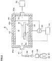
- FIG 2 schematically shows the state of a longitudinal section of an annealing unit 2.
- the sputtering unit 1 includes a processing container 10, for example, having an open upper portion and a bottomed cylindrical shape, and a lid body 11 with which the upper portion of the processing container 10 can be covered. By covering the upper portion of the processing container 10 with the lid body 11, a processing chamber S is formed.
- a mounting table 12 on which to mount a substrate, for example, a semiconductor wafer (hereinafter referred to as "a wafer") W as a processing object on which to form the ferroelectric film is provided at a bottom portion of the processing container 10.
- This mounting table 12 is provided with a suction means not shown, and thereby the mounting table 12 can hold the mounted wafer W by suction.
- a recessed portion 11a for example, is provided in a central portion of a ceiling surface of the processing chamber S facing the mounting table 12, that is, a lower surface of the lid body 11, and an electrode 13 is embedded in the recessed portion 11a.
- a voltage from a high-frequency source 14 provided outside the processing container 10 can be freely applied to the electrode 13.
- a target 15 is provided on a lower surface, that is, a surface facing the mounting table 12 of the electrode 13.
- a material for the target 15 is determined by the type of the ferroelectric film formed on the wafer W, and in this embodiment in which the ferroelectric film of STN (Sr 2 (Ta 1-x Nb x )O 7 (0 ⁇ x ⁇ 1)) is formed, Sr 2.5 (Ta 0.7 Nb 0.3 ) 2 0 7 having Sr, Ta, Nb as its main components is used as the material for the target 15.
- a processing gas introducing port 20 is provided, and a processing gas supply pipe 22 which leads to a processing gas supply source 21 is connected to the processing gas introducing port 20.
- a valve 23 and a mass flow controller 24 are provided in the processing gas supply pipe 22, and processing gas at a predetermined pressure can be supplied into the processing chamber S.
- respective supply sources 25 and 26 of oxygen gas (O 2 ) and argon (Ar) gas being a rare gas as the processing gas are connected to the processing gas supply source 21.
- the argon (Ar) gas another rare gas such as krypton (Kr), xenon (Xe), or the like may be used.
- an exhaust port 30 to exhaust the processing chamber S is provided in a side surface of the other end of the processing container 10 facing the above-described processing gas introducing port 20, an exhaust port 30 to exhaust the processing chamber S is provided.
- An exhaust pipe 32 which leads to an exhauster 31 such as a vacuum pump is connected to the exhaust port 30.
- the pressure in the processing chamber S for example, can be reduced to a predetermined pressure by the exhaust from the exhaust port 3 0.
- the processing gas supplied into the processing chamber S is turned into plasma by a high-frequency voltage of the electrode 13, and argon ions are produced.
- argon ions By maintaining the potential of the electrode 13 at a negative potential, positively charged argon ions fly toward the target 15 side and collide therewith.
- STN target species which are target atoms jump out of the target 15.
- a protective member formed of the same component material as the target 15 is attached to a portion with which the argon ions may collide, for example, a vicinity of the target 15 at the lower surface of the lid body 11.
- the protective film 35 is formed of a material of Sr 2.5 (Ta 0.7 Nb 0.3 ) 2 O 7 which has Sr, Ta, and Nb as its main components.
- the processing gas when the processing gas is turned into plasma, oxygen radicals are produced in the processing chamber S.
- the STN deposition species which have jumped out of the target 15 are oxidized by the oxygen radicals and deposited on the surface of the wafer W.
- a portion exposed to the oxygen radicals in the processing chamber S for example, a portion of an inner surface of the processing chamber S and higher than the height of the wafer W is coated with a quartz film K. By this quartz film K, the disappearance of the oxygen radicals is inhibited, and the STN deposition species in the processing chamber S are more certainly oxidized.
- the annealing unit 2 includes an almost cylindrical casing 40, for example, whose axis is directed horizontally as shown in FIG. 2.
- Side surface portions 40a and 40b of the casing 40 in an axial direction are closed by flanges, and a closed processing chamber H is formed in the casing 40.
- a mounting plate 41 to mount the wafer W on is provided in a central portion inside the casing 40.
- a cylinder portion 40c which covers a side surface of the casing 40 in a radial direction is formed thick, and heaters 42 are embedded therein.
- the heaters 42 are evenly embedded over the entire circumference of the cylinder portion 40c as shown in FIG 3 and can heat the wafer W on the mounting plate 41 uniformly from the entire circumferential direction.
- FIG. 1 As shown in FIG.
- the heaters 42 are connected to a power source 43 placed soutside the casing 40, and generate heat by power feeding from the power source 43.
- the power source 43 is controlled, for example, by a temperature controller 44, and the temperature controller 44 can control the temperature of the heaters 42 by changing power feeding output of the power source 43.
- a thermocouple T as a temperature sensor is provided in the mounting plate 41. A result of temperature measurement by the thermocouple T can be outputted to the temperature controller 44, and the temperature controller 44 can regulate the temperature of the heaters 42 based on this temperature measurement result.
- a processing gas introducing port 45 is bored in the side surface portion 40a of one end of the casing 40, and a processing gas supply pipe 47 which leads to a processing gas supply source 46 is connected to the processing gas introducing port 45.
- a valve 48 and a mass flow controller 49 are provided in the processing gas supply pipe 47, and processing gas at a predetermined pressure can be supplied into the processing chamber H.
- respective supply sources 50 and 51 of oxygen gas and argon gas as the processing gas are connected to the processing gas supply source 46.
- nitrogen gas (N 2 ) may be used.
- an exhaust port 53 leading to an exhauster 52 placed outside the casing 40 to exhaust an atmosphere in the processing chamber H is provided.
- the sputtering unit 1 and the annealing unit 2 have structures such as described above, and next, the ferroelectric film manufacturing method according to the embodiment of the present invention will be described with a case where a ferroelectric memory as a semiconductor device is manufactured as an example.
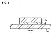
- the ferroelectric memory in this embodiment is, for example, a semiconductor memory using a field-effect transistor, and, for example, as shown in FIG. 4, a gate insulating film I as a gate of silicon oxide (SiO 2 ) is formed on a channel region R of the wafer W made of silicon (Si).
- a lower conductor film M 1 made of a metal oxide film, for example, an IrO 2 film is formed on the gate insulating film I.
- This lower conductor film M 1 is formed as a base film of the ferroelectric film described later. Incidentally, this lower conductor film M 1 may be formed by the same sputtering processing as the ferroelectric film described later.
- the wafer W on which the lower conductor film M 1 is formed is carried to the sputtering unit 1 and held on the mounting table 12 as shown in FIG 1.
- gas in the processing chamber S is exhausted from the exhaust port 30, and the pressure in the processing chamber S is reduced, for example, to approximately 4 Pa.
- the argon gas and the oxygen gas are supplied from the processing gas supply port 20, and the processing chamber S is filled with the argon gas and the oxygen gas.
- a negative potential high-frequency voltage is applied to the electrode 13, the gas in the processing chamber S is turned into plasma by this high-frequency voltage, and the argon gas is tuned into argon ions.
- the argon ions are attracted to the negative potential electrode 13 side and collide with the target 15 at high speed.
- the STN deposition species jump out of the target 15.
- the STN deposition species which have jumped out are oxidized by the oxygen radials produced by the oxygen gas being turned into plasma, and deposited on the surface of the wafer W.
- the wafer W is thus subjected to the sputtering processing, and as shown in FIG 5, a ferroelectric film F which uses STN as a film material is formed on the lower conductor film M 1 .
- the deposition of the STN deposition species is continued for a predetermined time and, for example, the 260-nm ferroelectric film F is formed on the lower conductor film M 1 , the application of the high-frequency voltage is stopped, and the sputtering processing in the sputtering unit 1 is completed.
- the wafer W is carried to the annealing unit 2 and mounted on the mounting plate 41 whose temperature is previously increased, for example, to 900°C by the heaters 42.
- the oxygen gas and the argon gas are introduced into the processing chamber H from the processing gas supply port 45, and gas in the processing chamber H is exhausted from the exhaust port 53.
- an atmospheric current flowing in the axial direction is formed in the processing chamber H, the interior of the processing chamber H continues to be purged, and a mixed gas atmosphere of the oxygen gas and the argon gas is substituted in the processing chamber H.
- the wafer W mounted on the mounting plate 41 which is maintained at 900°C is heated, and the ferroelectric film F is oxidized and crystallized.
- the ferroelectric film F is crystallized, the wafer W is taken out of the annealing unit 2, and annealing processing is completed.
- an upper conductor film M 2 such as shown in FIG. 6 is formed on the ferroelectric film F.
- This upper ferroelectric film M 2 is formed, for example, by the sputtering processing such as described above.
- the wafer W is carried again to the annealing unit 2 and heated in an oxygen gas atmosphere. Thereby, the surface of the ferroelectric film F is oxidized again, whereby a loss in the amount of oxygen component on the surface of the ferroelectric film F suffered when the upper conductor film M 2 is formed is recovered and made up. Thereafter, a photolithography process and the like are performed, and the field-effect transistor type ferroelectric memory is finished.
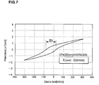
- FIG 7 shows a hysteresis characteristic of the ferroelectric film F, and a coercive electric field Ec of the ferroelectric film F is 52 kV/cm.
- FIG. 8 shows a C (Capacitance) - E (Electric field) characteristic of the ferroelectric film F, and on condition that a capacitor area S of the ferroelectric film F is 1.2 ⁇ 10 3 cm 2 and a film thickness df is 260 nm, a capacitance C of the ferroelectric film F is 1.44 ⁇ 10 -10 F.
- the unprecedented ferroelectric film F with a relative dielectric constant equal to or less than 40 and a coercive electric field exceeding 50 kV/cm can be formed.
- a reduction in relative dielectric constant and an increase in coercive electric field which are realized by the above-described method result from the attachment of the protective member 35 to the vicinity of the target 15.
- the protective member 35 can prevent deposition species other than STN from jumping out of the collision portion of the argon ions and being deposited on the wafer W, which can prevent the mixing of impurities into the ferroelectric film F.
- the high-purity film is formed, and the relative dielectric constant and the coercive electric field are improved.
- the metal oxide film is used as the base of the ferroelectric film F, which can prevent an outflow of the oxygen component from the ferroelectric film F through the base and a loss of the oxygen component of the ferroelectric film F. Consequently, Ta and Nb atoms in the ferroelectric film F are fully oxidized. In the ferroelectric memory using the ferroelectric film F thus manufactured, it becomes easy for the electric field to be applied to a capacitor portion, for example, composed of the ferroelectric film F and the conductor films M 1 and M 2 on both sides thereof.
- a polarization state of the ferroelectric film F can be created at a lower voltage, and a low power consumption semiconductor memory can be realized. Further, since the coercive electric field is large, the semiconductor memory with a stable polarization state can be realized.
- the ferroelectric film F is formed by one round of sputtering processing, but it is also possible to first form a thin lower ferroelectric film, introduce oxygen into the thin lower ferroelectric film by oxygen radicals, and then form a thick upper ferroelectric film. This case will be described as a second embodiment.
- FIG. 9 schematically shows the state of a longitudinal section of a plasma processing unit 60, and this plasma processing unit 60 is formed, for example, of an aluminum alloy.
- the plasma processing unit 60 includes an almost cylindrical processing container 61 having an opening in a ceiling portion. This processing container 61 is grounded. At a bottom portion of the processing container 61, a susceptor 62, for example, on which to mount the wafer W is provided.
- a heater 64 in the susceptor 62 generates heat by power feeding from an AC power source 63 provided outside the processing container 61, and thereby the wafer W on the susceptor 62 can be heated, for example, to approximately 400°C.
- an exhaust port 71 which leads to an exhauster 70 such as a turbo molecular pump, to exhaust gas in the processing container 61 is provided.
- the exhaust port 71 is provided, for example, close to a side surface portion of the processing container 61.
- a supply port 72 is provided in the ceiling portion of the processing container 61 on the opposite side of the exhaust port 71 across the susceptor 62.
- a supply pipe 74 which leads to a processing gas supply source 73 is connected to the supply port 72.
- respective supply sources 75 and 76 of oxygen gas and krypton (Kr) gas being a rare gas are connected to the processing gas supply source 73.
- the gases supplied into the processing container 61 from the supply port 72 pass over the wafer W on the susceptor 62 and exhausted from the exhaust port 71.
- another rare gas may be used.
- a dielectric window 81 for example, made of quartz glass is provided in the upper opening of the processing container 61 via a seal member 80 such as an O-ring to ensure hermeticity.
- a seal member 80 such as an O-ring to ensure hermeticity.
- An antenna member 82 is provided above the dielectric window 81.
- a coaxial waveguide 83 is connected to an upper portion of the antenna member 82.
- the coaxial waveguide 83 is connected to a microwave feeder 84 placed outside the processing container 61.
- a microwave of 2.45 GHz, for example, generated by the microwave feeder 84 is propagated to the antenna member 82 through the coaxial waveguide 83 and radiated into the processing space U via the dielectric window 81.
- a carry-in/out port 90 through which to carry the wafer W in/out and a shutter 91 to open/close the carry-in/out port 90 is provided in a side portion of the processing container 61.
- a dielectric film manufacturing method of the second embodiment will be described, and, for example, the wafer W on which the lower conductor film M 1 is formed is carried to the sputtering unit 1.
- a lower ferroelectric film F 1 as a thin film layer of 1 nm or more, for example, approximately 20 nm is formed on the lower conductor film M 1 , for example, as shown in FIG. 10.
- the wafer W is carried out of the sputtering unit 1 and carried to the plasma processing unit 60.
- the wafer W is carried in from the carry-in/out port 90, and as shown in FIG. 9, mounted on the susceptor 62 which is maintained, for example, at 400°C. Subsequently, a mixed gas of the oxygen gas and the krypton gas is supplied into the processing space U from the supply port 72, and a mixed gas atmosphere is substituted in the processing space U. Gas in the processing space U is exhausted from the exhaust pipe 71, and the pressure in the processing space U is reduced to a predetermined pressure, for example, approximately 133 Pa. Further, a microwave is generated by the microwave feeder 84, and this microwave is propagated to the antenna member 82.
- the mixed gas in the processing space U is turned into plasma by the microwave, and by oxygen radicals thereby produced in the processing space U, oxygen is introduced into the lower ferroelectric film F 1 as shown in FIG 11. Incidentally, at this time, a small amount of krypton component is also introduced into the lower ferroelectric film F 1 .
- the oxygen is introduced into the lower ferroelectric film F 1 by the oxygen radicals for a predetermined time, the radiation of the microwave from the antenna member 82 is stopped, and the wafer W is carried out of the plasma processing unit 60.
- the wafer W which has been carried out is carried again to the sputtering unit 1, and as shown in FIG. 12, a thicker upper ferroelectric film F 2 of approximately 240 nm is formed on the lower ferroelectric film F 1 .
- the dielectric film F (F 1 + F 2 ) having a two-layer structure is formed on the lower conductor film M 1 .
- the wafer W is carried to the annealing unit 2, the dielectric film F is crystallized, then the upper conductor film M 2 is formed in the same manner as in the above-described embodiment, and thereafter the wafer W is subjected to the annealing processing for oxygen recovery.
- FIG. 13 shows a comparison between hysteresis characteristics of the ferroelectric film F in a case where oxygen is introduced to the lower ferroelectric film F 1 by the plasma processing as in the above-described manufacturing method (with the plasma processing) and a case where oxygen is not introduced (without the plasma processing).
- FIG. 14 shows C-E characteristics in the cases with the plasma processing and without the plasma processing. Incidentally, in experimentation to collect this data, platinum which is a nonoxide is used for the lower conductor film M 1 being the base. As shown in FIG.
- a coercive electric field Ec 1 of the ferroelectric film F with the plasma processing is 35 kV/cm
- a coercive electric field Ec 2 of the ferroelectric film without the plasma processing is 17 kV/cm.
- the capacitance C is 1.95 ⁇ 10 -10 F on condition that the capacitor area S is 1.35 ⁇ 10 -3 cm 2 and the film thickness is 240 nm
- the capacitance C is 1.95 ⁇ 10 -10 F on condition that the capacitor area S is 1.2 ⁇ 10 -3 cm 2 and the film thickness is 240 nm.
- the lower ferroelectric film F 1 is formed, whereby even when a nonoxide which is apt to absorb the oxygen component is used as a material for the base of the ferroelectric film F, the outflow of the oxygen component is prevented, and thereby the ferroelectric film with a low relative electric constant and a high coercive electric field is formed. Moreover, by forming a thin film at a lower layer of the ferroelectric film F, the ferroelectric film which has a desired plane direction following a plane direction of the lower layer can be formed in an upper layer portion. Therefore, even if the base is amorphous, the good-quality ferroelectric film with a large coercive electric field is formed.
- an electric field may be applied to the ferroelectric film F when the temperature of the wafer W is increased to a Curie temperature of the ferroelectric film F and thereafter the temperature of the ferroelectric film F decreases and passes through the Curie temperature.
- a ferroelectric film manufacturing method in this case will be described as a third embodiment.
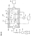
- an annealing unit 100 as a manufacturing unit used in the third embodiment as shown in FIG. 15, in addition to the structure of the above annealing unit 2, for example, a DC power source 101, an anode lead wire 102 of which one end is connected to an anode terminal of the DC power source 101 and the other end is connectable to the wafer W, and a cathode lead wire 103 of which one end is connected to a cathode terminal of the DC power source 101 and the other end is connectable to the wafer W are provided.
- an electric field applying part in this embodiment is composed of the DC power source 101, the anode lead wire 102, and the cathode lead wire 103, and a heating part is composed of the heaters 42, the AC power source 43, and the temperature controller 44.
- the other members of the annealing unit 100 are the same as those of the annealing unit 2, and a description thereof is omitted.
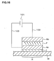
- the anode lead wire 102 is connected to the upper conductor film M 2 and the cathode lead wire 103 is connected to the lower conductor film M 1 as shown in FIG. 16.
- the DC power source 101 is OFF, and no electric field is added to the ferroelectric film F.
- the temperature of the wafer W is increased to a temperature higher than the Curie temperature of the ferroelectric film F, for example, approximately 900°C, by the heaters 42, and the amount of the oxygen component of the ferroelectric film F is recovered.
- the heaters 42 are powered off, and the wafer W is gradually cooled.
- the temperature of the wafer W is continuously measured, for example, by the thermocouple T.
- the DC power source 101 is turned on, and a voltage is applied between the upper conductor film M 2 and the lower conductor film M 1 .
- the process of applying the electric filed to the ferroelectric film F is performed at the time of heating processing for oxygen recovery, but it may be performed, for example, at the time of crystallization heating processing of crystallizing the ferroelectric film F or the sputtering processing of forming the ferroelectric film F.
- the processing of applying the electric field to the ferroelectric film such as described in the third embodiment is applicable to a case where instead of the sputtering method described above, for example, a sol-gel method, a CVD method, or the like is used as a method of forming the ferroelectric film, and even if any method is used, improvement in the characteristics of the ferroelectric film is realized.
- the annealing processing of recovering oxygen of the ferroelectric film F described in the above embodiments may be performed by oxidizing the oxygen radicals.
- the annealing processing of recovering oxygen may be performed using the above-described plasma processing unit 60.
- the wafer W on which the upper conductor film M 2 is formed is carried to the plasma processing unit 60 and mounted on the susceptor 62 maintained at a relatively low temperature of approximately 400°C. Then, the wafer W is heated at 400°C, and the processing gas in the processing space U is turned into plasma by the antenna member 82 and the oxygen radicals are produced.
- the ferroelectric film F is oxidized by the produced oxygen radicals, and oxygen is recovered.
- the oxidation is performed using the oxygen radicals having high oxidation capability, whereby the oxygen component of the ferroelectric film F can be recovered at a low temperature.
- ferroelectric film manufacturing methods described in the above embodiments are not limited to a case where the ferroelectric memory is manufactured and can be also applied to manufacturing of other semiconductor devices using the ferroelectric film.
- STN is used as a film material for the ferroelectric film
- the present invention is also applicable to a case of a mixed material of STN and PZT, SBT, or the like.
- the relative dielectric constant of the ferroelectric film is reduced, and the coercive electric filed thereof is increased, whereby, for example, using the ferroelectric film, a memory which is power-saving and whose polarization state is stable can be manufactured.
- the present invention is useful when concerning a ferroelectric film of Sr 2 (Ta 1-x Nb x )O 7 (0 ⁇ x ⁇ 1) which composes a semiconductor device such as a memory, its relative dielectric constant is reduced and coercive electric field is increased.
Landscapes
- Chemical & Material Sciences (AREA)
- Organic Chemistry (AREA)
- Inorganic Chemistry (AREA)
- Engineering & Computer Science (AREA)
- Mechanical Engineering (AREA)
- Materials Engineering (AREA)
- Chemical Kinetics & Catalysis (AREA)
- Metallurgy (AREA)
- Ceramic Engineering (AREA)
- Semiconductor Memories (AREA)
- Physical Vapour Deposition (AREA)
- Formation Of Insulating Films (AREA)
- Non-Volatile Memory (AREA)
- Inorganic Insulating Materials (AREA)
Applications Claiming Priority (3)
| Application Number | Priority Date | Filing Date | Title |
|---|---|---|---|
| JP2003028256A JP4346919B2 (ja) | 2003-02-05 | 2003-02-05 | 強誘電体膜,半導体装置及び強誘電体膜の製造装置 |
| JP2003028256 | 2003-02-05 | ||
| PCT/JP2004/001061 WO2004070736A1 (ja) | 2003-02-05 | 2004-02-03 | 強誘電体膜,半導体装置,強誘電体膜の製造方法及び強誘電体膜の製造装置 |
Publications (2)
| Publication Number | Publication Date |
|---|---|
| EP1594142A1 true EP1594142A1 (de) | 2005-11-09 |
| EP1594142A4 EP1594142A4 (de) | 2009-08-05 |
Family
ID=32844199
Family Applications (1)
| Application Number | Title | Priority Date | Filing Date |
|---|---|---|---|
| EP04707661A Withdrawn EP1594142A4 (de) | 2003-02-05 | 2004-02-03 | Ferroelektrischer film, halbleiterbauelement, herstellungsverfahren für einen ferroelektrischen film und herstellungsvorrichtung für einen ferroelektrischen film |
Country Status (6)
| Country | Link |
|---|---|
| US (1) | US20070034918A1 (de) |
| EP (1) | EP1594142A4 (de) |
| JP (1) | JP4346919B2 (de) |
| KR (2) | KR100811040B1 (de) |
| CN (2) | CN101215684B (de) |
| WO (1) | WO2004070736A1 (de) |
Cited By (1)
| Publication number | Priority date | Publication date | Assignee | Title |
|---|---|---|---|---|
| EP1820878A3 (de) * | 2006-01-20 | 2009-04-29 | Seiko Epson Corporation | Isolier-Targetmaterial, Verfahren zur Herstellung eines Isolier-Targetmaterials, leitfähiger komplexer Oxidfilm und Vorrichtung |
Families Citing this family (9)
| Publication number | Priority date | Publication date | Assignee | Title |
|---|---|---|---|---|
| US7220600B2 (en) * | 2004-12-17 | 2007-05-22 | Texas Instruments Incorporated | Ferroelectric capacitor stack etch cleaning methods |
| JP2006261159A (ja) * | 2005-03-15 | 2006-09-28 | Tohoku Univ | 強誘電体膜、金属酸化物、半導体装置、及びそれらの製造方法 |
| JP2008098474A (ja) * | 2006-10-13 | 2008-04-24 | Tokyo Electron Ltd | プラズマ処理装置とその運転方法、プラズマ処理方法および電子装置の製造方法 |
| KR100809367B1 (ko) | 2007-02-14 | 2008-03-05 | 한국과학기술연구원 | 강유전 박막의 강유전성 향상을 위한 전계 인가 열처리용튜브-로 및 이를 이용하여 강유전 박막의 강유전성을향상시키는 방법 |
| JP2009266967A (ja) * | 2008-04-23 | 2009-11-12 | Tohoku Univ | 強誘電体膜、強誘電体膜を有する半導体装置、及びそれらの製造方法 |
| CN102803357B (zh) | 2009-06-15 | 2014-07-09 | 株式会社村田制作所 | 压电体片以及压电体片的制造方法及制造装置 |
| CN112885755A (zh) * | 2021-03-11 | 2021-06-01 | 铜仁学院 | 一种铁电薄膜的退火方法及装置 |
| US12062584B1 (en) * | 2022-10-28 | 2024-08-13 | Kepler Computing Inc. | Iterative method of multilayer stack development for device applications |
| CN119947571A (zh) * | 2025-01-09 | 2025-05-06 | 西安电子科技大学 | 一种低热预算铁电二极管内容可寻址存储器及其制备方法 |
Family Cites Families (9)
| Publication number | Priority date | Publication date | Assignee | Title |
|---|---|---|---|---|
| JP3261179B2 (ja) * | 1992-11-19 | 2002-02-25 | 株式会社トキメック | 薄膜製造装置 |
| JP3480624B2 (ja) * | 1995-06-09 | 2003-12-22 | シャープ株式会社 | 強誘電体薄膜被覆基板、その製造方法、及びキャパシタ構造素子 |
| JP3190011B2 (ja) * | 1997-05-23 | 2001-07-16 | ローム株式会社 | 強誘電体記憶素子およびその製造方法 |
| US6410343B1 (en) * | 1999-04-28 | 2002-06-25 | Sharp Laboratories Of America, Inc. | C-axis oriented lead germanate film and deposition method |
| CN1358326A (zh) * | 1999-06-10 | 2002-07-10 | 塞姆特里克斯公司 | 高介电常数的金属氧化物薄膜 |
| JP2001354497A (ja) * | 2000-06-07 | 2001-12-25 | Matsushita Electric Ind Co Ltd | 強誘電体膜の製造方法 |
| JP2002057155A (ja) * | 2000-08-08 | 2002-02-22 | Fujitsu Ltd | 5酸化タンタル膜の製造方法 |
| US6717195B2 (en) * | 2001-06-29 | 2004-04-06 | Rohm Co., Ltd. | Ferroelectric memory |
| TWI233506B (en) * | 2004-05-20 | 2005-06-01 | Univ Nat Sun Yat Sen | Method and apparatus for fabricating a crystal fiber |
-
2003
- 2003-02-05 JP JP2003028256A patent/JP4346919B2/ja not_active Expired - Fee Related
-
2004
- 2004-02-03 CN CN2007101986361A patent/CN101215684B/zh not_active Expired - Fee Related
- 2004-02-03 EP EP04707661A patent/EP1594142A4/de not_active Withdrawn
- 2004-02-03 WO PCT/JP2004/001061 patent/WO2004070736A1/ja not_active Ceased
- 2004-02-03 KR KR1020077008442A patent/KR100811040B1/ko not_active Expired - Fee Related
- 2004-02-03 KR KR1020057014386A patent/KR100732930B1/ko not_active Expired - Fee Related
- 2004-02-03 US US10/544,559 patent/US20070034918A1/en not_active Abandoned
- 2004-02-03 CN CNB2004800036506A patent/CN100483566C/zh not_active Expired - Fee Related
Cited By (2)
| Publication number | Priority date | Publication date | Assignee | Title |
|---|---|---|---|---|
| EP1820878A3 (de) * | 2006-01-20 | 2009-04-29 | Seiko Epson Corporation | Isolier-Targetmaterial, Verfahren zur Herstellung eines Isolier-Targetmaterials, leitfähiger komplexer Oxidfilm und Vorrichtung |
| US7867472B2 (en) | 2006-01-20 | 2011-01-11 | Seiko Epson Corporation | Insulating target material, method of manufacturing insulating target material, conductive complex oxide film, and device |
Also Published As
| Publication number | Publication date |
|---|---|
| JP4346919B2 (ja) | 2009-10-21 |
| KR100732930B1 (ko) | 2007-06-29 |
| US20070034918A1 (en) | 2007-02-15 |
| CN101215684B (zh) | 2010-09-01 |
| KR20070049686A (ko) | 2007-05-11 |
| CN100483566C (zh) | 2009-04-29 |
| CN101215684A (zh) | 2008-07-09 |
| EP1594142A4 (de) | 2009-08-05 |
| KR100811040B1 (ko) | 2008-03-07 |
| CN1748264A (zh) | 2006-03-15 |
| WO2004070736A1 (ja) | 2004-08-19 |
| JP2004265915A (ja) | 2004-09-24 |
| KR20050100657A (ko) | 2005-10-19 |
Similar Documents
| Publication | Publication Date | Title |
|---|---|---|
| EP1265276B1 (de) | Verfahren zur ausbildung eines dielektrischen films | |
| JP2596214B2 (ja) | 高純度薄膜の形成方法 | |
| JP4493208B2 (ja) | 不揮発性メモリ素子及びその製造方法 | |
| US20100120238A1 (en) | Semiconductor manufacturing apparatus and method | |
| EP1634324A1 (de) | Verfahren und vorrichtung für plasmanitrierung eines gate-dielektrikums durch eine amplitudemodulierte radiofrequenzenergie | |
| US9224594B2 (en) | Surface preparation with remote plasma | |
| US20050255711A1 (en) | Method for forming underlying insulation film | |
| US10347492B2 (en) | Modifying work function of a metal film with a plasma process | |
| EP1594142A1 (de) | Ferroelektrischer film, halbleiterbauelement, herstellungsverfahren für einen ferroelektrischen film und herstellungsvorrichtung für einen ferroelektrischen film | |
| EP1030352A2 (de) | Verfahren und Apparat zum Herstellen von Materialenschichten mittels atomarer Gase | |
| US7736446B2 (en) | Method for manufacturing a lanthanum oxide compound | |
| US20030116795A1 (en) | Method of manufacturing a tantalum pentaoxide - aluminum oxide film and semiconductor device using the film | |
| US20090267122A1 (en) | Semiconductor device and method of manufacturing the semiconductor device | |
| JP2010016127A (ja) | 強誘電体膜、強誘電体膜を有する半導体装置、及びそれらの製造方法 | |
| JP5300017B2 (ja) | 強誘電体膜の製造方法と、強誘電体膜を用いた半導体装置 | |
| JP2006261159A (ja) | 強誘電体膜、金属酸化物、半導体装置、及びそれらの製造方法 | |
| JP2002299332A (ja) | プラズマ成膜方法及びプラズマcvd装置 | |
| US7157334B2 (en) | Method of manufacturing flash memory device | |
| Chung et al. | Microstructure and electric properties of the PZT thin films fabricated by ECR PECVD: the effects of an interfacial layer and rapid thermal annealing | |
| KR100793471B1 (ko) | 반도체 장치 및 그 제조 방법 | |
| JP2003060167A (ja) | 強誘電体メモリおよびその製造方法 |
Legal Events
| Date | Code | Title | Description |
|---|---|---|---|
| PUAI | Public reference made under article 153(3) epc to a published international application that has entered the european phase |
Free format text: ORIGINAL CODE: 0009012 |
|
| 17P | Request for examination filed |
Effective date: 20050830 |
|
| AK | Designated contracting states |
Kind code of ref document: A1 Designated state(s): AT BE BG CH CY CZ DE DK EE ES FI FR GB GR HU IE IT LI LU MC NL PT RO SE SI SK TR |
|
| AX | Request for extension of the european patent |
Extension state: AL LT LV MK |
|
| DAX | Request for extension of the european patent (deleted) | ||
| RBV | Designated contracting states (corrected) |
Designated state(s): DE FR GB IT NL |
|
| A4 | Supplementary search report drawn up and despatched |
Effective date: 20090707 |
|
| 17Q | First examination report despatched |
Effective date: 20090921 |
|
| STAA | Information on the status of an ep patent application or granted ep patent |
Free format text: STATUS: THE APPLICATION IS DEEMED TO BE WITHDRAWN |
|
| 18D | Application deemed to be withdrawn |
Effective date: 20100202 |