EP1593450A1 - Electronic device with surface mount components having stand-off space free of solder mask under the component - method for manfacturing the same - Google Patents
Electronic device with surface mount components having stand-off space free of solder mask under the component - method for manfacturing the same Download PDFInfo
- Publication number
- EP1593450A1 EP1593450A1 EP05252728A EP05252728A EP1593450A1 EP 1593450 A1 EP1593450 A1 EP 1593450A1 EP 05252728 A EP05252728 A EP 05252728A EP 05252728 A EP05252728 A EP 05252728A EP 1593450 A1 EP1593450 A1 EP 1593450A1
- Authority
- EP
- European Patent Office
- Prior art keywords
- component
- substrate
- solder
- smt
- stand
- Prior art date
- Legal status (The legal status is an assumption and is not a legal conclusion. Google has not performed a legal analysis and makes no representation as to the accuracy of the status listed.)
- Withdrawn
Links
- 238000000034 method Methods 0.000 title claims abstract description 20
- 229910000679 solder Inorganic materials 0.000 title claims description 64
- 238000004140 cleaning Methods 0.000 claims abstract description 22
- 239000012530 fluid Substances 0.000 claims abstract description 13
- 238000004519 manufacturing process Methods 0.000 claims abstract description 3
- 239000000758 substrate Substances 0.000 claims description 42
- 229920000642 polymer Polymers 0.000 claims description 5
- 239000000919 ceramic Substances 0.000 claims description 2
- 238000005476 soldering Methods 0.000 claims description 2
- 238000000151 deposition Methods 0.000 claims 1
- 239000004020 conductor Substances 0.000 description 11
- 238000005516 engineering process Methods 0.000 description 4
- 230000001965 increasing effect Effects 0.000 description 4
- 239000000463 material Substances 0.000 description 4
- 230000000694 effects Effects 0.000 description 3
- 238000012986 modification Methods 0.000 description 3
- 230000004048 modification Effects 0.000 description 3
- 238000010586 diagram Methods 0.000 description 2
- 239000003822 epoxy resin Substances 0.000 description 2
- 229910052751 metal Inorganic materials 0.000 description 2
- 239000002184 metal Substances 0.000 description 2
- 239000003960 organic solvent Substances 0.000 description 2
- 229920000647 polyepoxide Polymers 0.000 description 2
- 239000011800 void material Substances 0.000 description 2
- 238000009736 wetting Methods 0.000 description 2
- RYGMFSIKBFXOCR-UHFFFAOYSA-N Copper Chemical compound [Cu] RYGMFSIKBFXOCR-UHFFFAOYSA-N 0.000 description 1
- 241000272168 Laridae Species 0.000 description 1
- 239000004642 Polyimide Substances 0.000 description 1
- 230000002378 acidificating effect Effects 0.000 description 1
- 239000000654 additive Substances 0.000 description 1
- 230000000996 additive effect Effects 0.000 description 1
- 229910052782 aluminium Inorganic materials 0.000 description 1
- XAGFODPZIPBFFR-UHFFFAOYSA-N aluminium Chemical compound [Al] XAGFODPZIPBFFR-UHFFFAOYSA-N 0.000 description 1
- 238000013459 approach Methods 0.000 description 1
- 239000003990 capacitor Substances 0.000 description 1
- 239000000969 carrier Substances 0.000 description 1
- 239000003795 chemical substances by application Substances 0.000 description 1
- 229910052802 copper Inorganic materials 0.000 description 1
- 239000010949 copper Substances 0.000 description 1
- 239000003599 detergent Substances 0.000 description 1
- 230000002708 enhancing effect Effects 0.000 description 1
- 238000000465 moulding Methods 0.000 description 1
- 238000012856 packing Methods 0.000 description 1
- 239000002245 particle Substances 0.000 description 1
- 238000000206 photolithography Methods 0.000 description 1
- 229920002120 photoresistant polymer Polymers 0.000 description 1
- 229920000058 polyacrylate Polymers 0.000 description 1
- 229920001721 polyimide Polymers 0.000 description 1
- 238000007650 screen-printing Methods 0.000 description 1
- 229910052710 silicon Inorganic materials 0.000 description 1
- 239000010703 silicon Substances 0.000 description 1
Images


Classifications
-
- B—PERFORMING OPERATIONS; TRANSPORTING
- B23—MACHINE TOOLS; METAL-WORKING NOT OTHERWISE PROVIDED FOR
- B23K—SOLDERING OR UNSOLDERING; WELDING; CLADDING OR PLATING BY SOLDERING OR WELDING; CUTTING BY APPLYING HEAT LOCALLY, e.g. FLAME CUTTING; WORKING BY LASER BEAM
- B23K1/00—Soldering, e.g. brazing, or unsoldering
- B23K1/0008—Soldering, e.g. brazing, or unsoldering specially adapted for particular articles or work
- B23K1/0016—Brazing of electronic components
-
- H—ELECTRICITY
- H01—ELECTRIC ELEMENTS
- H01L—SEMICONDUCTOR DEVICES NOT COVERED BY CLASS H10
- H01L21/00—Processes or apparatus adapted for the manufacture or treatment of semiconductor or solid state devices or of parts thereof
- H01L21/02—Manufacture or treatment of semiconductor devices or of parts thereof
- H01L21/04—Manufacture or treatment of semiconductor devices or of parts thereof the devices having potential barriers, e.g. a PN junction, depletion layer or carrier concentration layer
- H01L21/50—Assembly of semiconductor devices using processes or apparatus not provided for in a single one of the groups H01L21/18 - H01L21/326 or H10D48/04 - H10D48/07 e.g. sealing of a cap to a base of a container
- H01L21/52—Mounting semiconductor bodies in containers
-
- H—ELECTRICITY
- H05—ELECTRIC TECHNIQUES NOT OTHERWISE PROVIDED FOR
- H05K—PRINTED CIRCUITS; CASINGS OR CONSTRUCTIONAL DETAILS OF ELECTRIC APPARATUS; MANUFACTURE OF ASSEMBLAGES OF ELECTRICAL COMPONENTS
- H05K3/00—Apparatus or processes for manufacturing printed circuits
- H05K3/22—Secondary treatment of printed circuits
- H05K3/26—Cleaning or polishing of the conductive pattern
-
- H—ELECTRICITY
- H05—ELECTRIC TECHNIQUES NOT OTHERWISE PROVIDED FOR
- H05K—PRINTED CIRCUITS; CASINGS OR CONSTRUCTIONAL DETAILS OF ELECTRIC APPARATUS; MANUFACTURE OF ASSEMBLAGES OF ELECTRICAL COMPONENTS
- H05K3/00—Apparatus or processes for manufacturing printed circuits
- H05K3/30—Assembling printed circuits with electric components, e.g. with resistor
- H05K3/32—Assembling printed circuits with electric components, e.g. with resistor electrically connecting electric components or wires to printed circuits
- H05K3/34—Assembling printed circuits with electric components, e.g. with resistor electrically connecting electric components or wires to printed circuits by soldering
- H05K3/3452—Solder masks
-
- B—PERFORMING OPERATIONS; TRANSPORTING
- B23—MACHINE TOOLS; METAL-WORKING NOT OTHERWISE PROVIDED FOR
- B23K—SOLDERING OR UNSOLDERING; WELDING; CLADDING OR PLATING BY SOLDERING OR WELDING; CUTTING BY APPLYING HEAT LOCALLY, e.g. FLAME CUTTING; WORKING BY LASER BEAM
- B23K2101/00—Articles made by soldering, welding or cutting
- B23K2101/36—Electric or electronic devices
- B23K2101/42—Printed circuits
-
- H—ELECTRICITY
- H01—ELECTRIC ELEMENTS
- H01L—SEMICONDUCTOR DEVICES NOT COVERED BY CLASS H10
- H01L2224/00—Indexing scheme for arrangements for connecting or disconnecting semiconductor or solid-state bodies and methods related thereto as covered by H01L24/00
- H01L2224/01—Means for bonding being attached to, or being formed on, the surface to be connected, e.g. chip-to-package, die-attach, "first-level" interconnects; Manufacturing methods related thereto
- H01L2224/10—Bump connectors; Manufacturing methods related thereto
- H01L2224/15—Structure, shape, material or disposition of the bump connectors after the connecting process
- H01L2224/16—Structure, shape, material or disposition of the bump connectors after the connecting process of an individual bump connector
- H01L2224/161—Disposition
- H01L2224/16151—Disposition the bump connector connecting between a semiconductor or solid-state body and an item not being a semiconductor or solid-state body, e.g. chip-to-substrate, chip-to-passive
- H01L2224/16221—Disposition the bump connector connecting between a semiconductor or solid-state body and an item not being a semiconductor or solid-state body, e.g. chip-to-substrate, chip-to-passive the body and the item being stacked
- H01L2224/16225—Disposition the bump connector connecting between a semiconductor or solid-state body and an item not being a semiconductor or solid-state body, e.g. chip-to-substrate, chip-to-passive the body and the item being stacked the item being non-metallic, e.g. insulating substrate with or without metallisation
-
- H—ELECTRICITY
- H05—ELECTRIC TECHNIQUES NOT OTHERWISE PROVIDED FOR
- H05K—PRINTED CIRCUITS; CASINGS OR CONSTRUCTIONAL DETAILS OF ELECTRIC APPARATUS; MANUFACTURE OF ASSEMBLAGES OF ELECTRICAL COMPONENTS
- H05K2201/00—Indexing scheme relating to printed circuits covered by H05K1/00
- H05K2201/09—Shape and layout
- H05K2201/09818—Shape or layout details not covered by a single group of H05K2201/09009 - H05K2201/09809
- H05K2201/0989—Coating free areas, e.g. areas other than pads or lands free of solder resist
-
- H—ELECTRICITY
- H05—ELECTRIC TECHNIQUES NOT OTHERWISE PROVIDED FOR
- H05K—PRINTED CIRCUITS; CASINGS OR CONSTRUCTIONAL DETAILS OF ELECTRIC APPARATUS; MANUFACTURE OF ASSEMBLAGES OF ELECTRICAL COMPONENTS
- H05K2201/00—Indexing scheme relating to printed circuits covered by H05K1/00
- H05K2201/09—Shape and layout
- H05K2201/09818—Shape or layout details not covered by a single group of H05K2201/09009 - H05K2201/09809
- H05K2201/09909—Special local insulating pattern, e.g. as dam around component
-
- H—ELECTRICITY
- H05—ELECTRIC TECHNIQUES NOT OTHERWISE PROVIDED FOR
- H05K—PRINTED CIRCUITS; CASINGS OR CONSTRUCTIONAL DETAILS OF ELECTRIC APPARATUS; MANUFACTURE OF ASSEMBLAGES OF ELECTRICAL COMPONENTS
- H05K2201/00—Indexing scheme relating to printed circuits covered by H05K1/00
- H05K2201/10—Details of components or other objects attached to or integrated in a printed circuit board
- H05K2201/10613—Details of electrical connections of non-printed components, e.g. special leads
- H05K2201/10621—Components characterised by their electrical contacts
- H05K2201/10689—Leaded Integrated Circuit [IC] package, e.g. dual-in-line [DIL]
-
- H—ELECTRICITY
- H05—ELECTRIC TECHNIQUES NOT OTHERWISE PROVIDED FOR
- H05K—PRINTED CIRCUITS; CASINGS OR CONSTRUCTIONAL DETAILS OF ELECTRIC APPARATUS; MANUFACTURE OF ASSEMBLAGES OF ELECTRICAL COMPONENTS
- H05K2201/00—Indexing scheme relating to printed circuits covered by H05K1/00
- H05K2201/10—Details of components or other objects attached to or integrated in a printed circuit board
- H05K2201/10613—Details of electrical connections of non-printed components, e.g. special leads
- H05K2201/10621—Components characterised by their electrical contacts
- H05K2201/10727—Leadless chip carrier [LCC], e.g. chip-modules for cards
-
- H—ELECTRICITY
- H05—ELECTRIC TECHNIQUES NOT OTHERWISE PROVIDED FOR
- H05K—PRINTED CIRCUITS; CASINGS OR CONSTRUCTIONAL DETAILS OF ELECTRIC APPARATUS; MANUFACTURE OF ASSEMBLAGES OF ELECTRICAL COMPONENTS
- H05K3/00—Apparatus or processes for manufacturing printed circuits
- H05K3/30—Assembling printed circuits with electric components, e.g. with resistor
- H05K3/32—Assembling printed circuits with electric components, e.g. with resistor electrically connecting electric components or wires to printed circuits
- H05K3/34—Assembling printed circuits with electric components, e.g. with resistor electrically connecting electric components or wires to printed circuits by soldering
- H05K3/341—Surface mounted components
- H05K3/3421—Leaded components
-
- H—ELECTRICITY
- H05—ELECTRIC TECHNIQUES NOT OTHERWISE PROVIDED FOR
- H05K—PRINTED CIRCUITS; CASINGS OR CONSTRUCTIONAL DETAILS OF ELECTRIC APPARATUS; MANUFACTURE OF ASSEMBLAGES OF ELECTRICAL COMPONENTS
- H05K3/00—Apparatus or processes for manufacturing printed circuits
- H05K3/30—Assembling printed circuits with electric components, e.g. with resistor
- H05K3/32—Assembling printed circuits with electric components, e.g. with resistor electrically connecting electric components or wires to printed circuits
- H05K3/34—Assembling printed circuits with electric components, e.g. with resistor electrically connecting electric components or wires to printed circuits by soldering
- H05K3/341—Surface mounted components
- H05K3/3431—Leadless components
- H05K3/3442—Leadless components having edge contacts, e.g. leadless chip capacitors, chip carriers
Definitions
- This invention relates to surface mount technology (SMT) and to methods for mounting SMT components that promote improved post-solder cleaning.
- SMT surface mount technology
- PCBs printed circuit boards
- DIP dual-in-line package
- SMT Surface Mount Technology
- SMT mounting has a variety of forms. Many address mounting discrete components for hybrid circuits. Typical components are capacitors, resistors, inductors, LEDs, discrete transistors, etc. Sub-circuit or sub-assembly packages with combinations of these elements are also commonly packaged as SMT components. For example, filters and other RC circuits are often packaged as a single unit.
- Integrated circuit devices, with large numbers of devices, both passive devices and active transistors, are often mounted using SMT.
- solder In attaching the components to the board surface, solder is the nearly universal attachment medium. This allows the attachment to also serve as an electrical interconnection. Electrical contacts on the component are soldered to conductor pads on the board. Electrical contacts on the component may be leadless, i.e. flat pre-tinned surface, or may be leads that extend from the component package. Leads on leaded chip carrier packages typically have distinct shapes, e.g. gull-wing, J-shaped, I-shaped.
- solder operation typically creates residue and debris. Residue is produced by solder fluxing agents, which are acidic, corrosive, and can contain ionic components that conduct electric signals. If not fully removed, these residues can lead to product reliability problems. Debris may comprise small particles of solder and/or other materials that form during the solder reflow steps, which also may be harmful to the finished device. Accordingly, SMT solder operations usually conclude with a cleaning step, wherein a fluid is circulated around the mounted devices. The flow of cleaning fluid also penetrates into the space between the component and the board, a space that often contains the harmful residue and debris.
- the space between the bottom of the component and the board or substrate is referred to below as the stand-off space, and the distance separating the substrate surface and the bottom of the component is referred to as the stand-off height.
- the stand-off height is determined by the vertical distance between the top surface of the soldermask layer and the bottom surface of the component package.
- the stand-off space is nominally controlled by the size and shape of the leads.
- the standoff is determined largely by the surface tension and collapse height of the solder during reflow.
- the stand-off space becomes more confined.
- the confined space is both more prone to trapping of residue and debris, and more inaccessible to the flow of cleaning fluid. Accordingly, where the stand-off space is very confined, the cleaning operation may be ineffective.
- the stand-off space can be enlarged significantly by selectively omitting, or selectively removing, the soldermask underneath the component package.
- the region on the substrate underneath the component package, where the component is soldered, is referred to here as the component footprint. It is typically square or rectangular.
- the stand-off height is increased by the thickness the omitted soldermask would have consumed.
- the stand-off height is typically small, and the thickness of the soldermask is a significant fraction of the stand-off height.
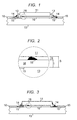
- a leaded component 11, with gull-wing leads 12 is shown surface mounted to substrate 13 by solder fillets 14.
- the structure relevant to the description of the invention is shown in section (the internal features of the component are not).
- Under the solder fillets are conductor pads 15.
- the conductor pads are integral with circuit runners that interconnect multiple components on the board.
- the conductor pads are typically copper, but may be aluminum or another metal with some form of top plated metal to insure wetting of the conductor pads by the applied solder.
- Fig. 1 is representative of a common SMT method wherein a soldermask, here shown at 16, is used to selectively confine the location of solder on the substrate. Debris resulting from the soldering operation is shown at 18, trapped in the stand-off space between the soldermask layer 16, and the bottom of the component 11.
- Fig. 2 shows the dashed circle portion of Fig. 1, and shows the stand-off space in more detail.
- the thickness of the soldermask layer is designated t in this figure.
- the standoff height S is nominally determined by the size and shape of leads 12. The leads either contact the surface of the substrate 13, or, if the component is very small may float slightly above the surface of the substrate.
- the nominal stand-off height as related to the solder sites is determined by the substrate surface, and has a maximum height of S.
- the stand-off height underneath the component 11 is determined not by the surface of substrate 13, but by the surface of the soldermask layer 16. Accordingly, the actual stand-off height is g in Fig. 2. As mentioned earlier, this stand-off height grows smaller as device size shrinks.
- Fig. 2 shows debris 18 firmly trapped in the gap g.
- Figs. 1 and 2 illustrate in general the problem of debris or residue trapped or formed in the stand-off space. While the component shown here is a leaded package with gull-wing leads, the problem is broadly encountered in a wide variety of discrete component and integrated circuit packages.
- Fig. 3 shows the problem in a leadless surface mount component. All elements are the same as in Fig. 1 except there are no leads 12.
- the stand-off under the surface mount component is determined largely by the solder surface-tension/collapse characteristics during solder reflow.
- the ends of the component are typically tinned (not shown) to promote wetting between the component and the conductor pads.
- Fig. 4 is another SMT package type, wherein solder bumps or BGA balls 24 are used for attaching the device 11.
- the device 11 in BGA technology is an integrated circuit, and the number of balls, or interconnections, can be very large.
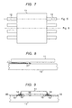
- Fig. 5 shows the package of Fig. 1 with the soldermask omitted from the region approximately corresponding to the component footprint. Soldermask 16 still remains surrounding the solder sites as shown. The effect of omitting the solder mask from the component footprint is evident in Fig. 6, where the gap g between the bottom of component 11 and the substrate is equivalent to the maximum stand-off shown in Fig. 2, thus significantly enhancing access to the stand-off space by the cleaning fluid during the post-solder cleaning operation.
- Fig. 5 shows a section through the leads 12 of the component 11, i.e. along line denoted "Fig. 5" in Fig. 7.
- the view between the leads, denoted by section line “Fig. 8" in Fig. 7, is shown in Fig. 8.
- Flow of cleaning fluid is represented by the arrows, and dislodged debris is shown at 31. It is seen that the flow of cleaning fluid is unhindered by a soldermask.
- Fig. 9 shows the embodiment of Fig. 3, an SMT leadless chip carrier (LCC), with the soldermask omitted from the component footprint
- Fig. 10 shows the embodiment of Fig. 4 with the soldermask omitted from the footprint. In each case, the same effect as that described for Fig. 5 is evident.
- LCC leadless chip carrier
- the soldermask layer is typically a polymer, for example, a polyimide, a polyacrylate, or suitable alternative. Preferably, it is a photoimageable polymer.
- the soldermask material is preferably blanket deposited on the substrate, and patterned using photolithography. A wide variety of photoresist type materials are known in the art, and these types of materials are easily applied and patterned by well known and well developed techniques. The layer is masked, exposed, and developed. Alternative methods, for example additive methods like screen printing, may also be used.
- Fig. 11 shows a plan view of a soldermask layer 41, patterned according to prior art teachings, to cover the substrate except in the solder sites 42.
- the component outline is shown in phantom at 45, with the component leads shown at 46. Also, a conductor pad 47 is shown in phantom. For clarity, only one conductor pad is shown, it being understood that a conductor pad underlies each solder site 42.
- the spacing between leads may be larger than that shown, to allow for some misalignment between the leads and the conductor pads.
- the conductor pads are typically made larger than the leads so that the base of the gull-wing resides entirely on the pads.
- the photomask for producing the soldermask appears much like Fig. 11, with a pattern of openings corresponding to the solder sites.
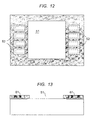
- soldermask for implementing the invention is shown in Fig. 12, with opening 51, corresponding approximately to the component footprint. Solder site windows 52 are provided as shown.
- solder paste operation is performed in the usual manner except that paste is selectively applied to the solder site windows 52, and omitted in the region of the component footprint.
- solder paste 61 is selectively deposited in the solder site windows.
- Selective application of solder paste may be easily implemented using a well known stencil method.
- the stencil is provided with openings for the solder sites but no opening in the component footprint region.
- the solder paste is then reflowed to produce solder bumps as shown at 71 in Fig. 14. Suitable solder bumps may also be produced by other methods. For example, solder may be evaporated through a shadow mask.
- the cleaning fluid may be any of many well known organic solvents or detergents.
- Fig. 7 shows an embodiment where the open spaces on the ends of the soldermask may be extended to expand the void space.
- Fig. 16 shows extended void regions 51 a enlarge the component footprint to increase access to the region underneath the component.
- Fig. 17 shows an embodiment where the component, shown in phantom outline 81, has leads on all four sides.
- the opening in the soldermask underneath the component is made slightly larger than the component footprint and, additionally, one or more channels 82 are provided to increase accessibility of the cleaning fluid to the region underneath the component.
- PCBs are typically epoxy resin boards, e.g. FR4. They may be single or multilayer. Mounting substrates may also be ceramic or silicon.
- soldermask in the region of the component footprint is a simple implementation of the invention
- other step sequences may achieve equivalent results. It is only important that the soldermask under the component be absent during the cleaning operation. Accordingly, the soldermask in the component footprint may be etched away in a separate step. This sequence may be useful if solder paste is applied with a squeegee, making it more difficult to confine the solder paste to just the solder sites. In that case, the conventional soldermask may be formed, the solder paste deposited and reflowed, then the component footprint region of the soldermask removed. There are several well known organic solvents available to selectively etch the soldermask.
- the stand-off space is enhanced by removing a portion of the soldermask.
- An alternative to this is to remove portions of the substrate, or to shape the substrate, thereby increasing the stand-off height.
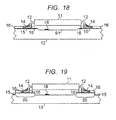
- Two embodiments for achieving this result are shown in Figs. 18 and 19.
- the area of the top surface of the substrate under the component footprint is selectively etched to form a depression 91 in the substrate.
- the soldermask can be present or omitted by choice.
- the stand-off height is increased by the depth of the etched depression.
- the substrate can be manufactured with pre-fabricated depressions. Forming a circuit board with depressions suitably located on the board is straightforward, especially since the circuit board is typically formed by a molding process.
- Fig. 19 represents embodiments where the substrate is molded with raised portions 95. These are located at the solder sites and function to raise the component from the board surface, thus achieving the objective of increasing the stand-off height.
Landscapes
- Engineering & Computer Science (AREA)
- Manufacturing & Machinery (AREA)
- Microelectronics & Electronic Packaging (AREA)
- Mechanical Engineering (AREA)
- Physics & Mathematics (AREA)
- Condensed Matter Physics & Semiconductors (AREA)
- General Physics & Mathematics (AREA)
- Computer Hardware Design (AREA)
- Power Engineering (AREA)
- Electric Connection Of Electric Components To Printed Circuits (AREA)
- Manufacturing Of Printed Wiring (AREA)
Applications Claiming Priority (2)
| Application Number | Priority Date | Filing Date | Title |
|---|---|---|---|
| US838897 | 2004-05-04 | ||
| US10/838,897 US20050247761A1 (en) | 2004-05-04 | 2004-05-04 | Surface mount attachment of components |
Publications (1)
| Publication Number | Publication Date |
|---|---|
| EP1593450A1 true EP1593450A1 (en) | 2005-11-09 |
Family
ID=34941133
Family Applications (1)
| Application Number | Title | Priority Date | Filing Date |
|---|---|---|---|
| EP05252728A Withdrawn EP1593450A1 (en) | 2004-05-04 | 2005-05-03 | Electronic device with surface mount components having stand-off space free of solder mask under the component - method for manfacturing the same |
Country Status (6)
| Country | Link |
|---|---|
| US (2) | US20050247761A1 (enExample) |
| EP (1) | EP1593450A1 (enExample) |
| JP (1) | JP2005322915A (enExample) |
| KR (1) | KR20060047725A (enExample) |
| CN (1) | CN1741715A (enExample) |
| TW (1) | TW200607422A (enExample) |
Families Citing this family (13)
| Publication number | Priority date | Publication date | Assignee | Title |
|---|---|---|---|---|
| US6889568B2 (en) | 2002-01-24 | 2005-05-10 | Sensarray Corporation | Process condition sensing wafer and data analysis system |
| US7721238B2 (en) * | 2004-09-22 | 2010-05-18 | Digi International Inc. | Method and apparatus for configurable printed circuit board circuit layout pattern |
| ATE397310T1 (de) * | 2005-11-01 | 2008-06-15 | Black & Decker Inc | Kodiereinheit mit widerständen für einen kabelbaum |
| US8604361B2 (en) * | 2005-12-13 | 2013-12-10 | Kla-Tencor Corporation | Component package for maintaining safe operating temperature of components |
| CN101990364B (zh) * | 2009-08-04 | 2012-05-09 | 纬创资通股份有限公司 | 组装组件至电路板的方法与相关电路板组装系统 |
| WO2011161552A2 (en) | 2010-06-14 | 2011-12-29 | Black & Decker Inc. | Control unit for brushless motor in a power tool |
| US9450471B2 (en) | 2012-05-24 | 2016-09-20 | Milwaukee Electric Tool Corporation | Brushless DC motor power tool with combined PCB design |
| JP6036303B2 (ja) * | 2013-01-07 | 2016-11-30 | セイコーエプソン株式会社 | パッケージ、光学モジュール、及び電子機器 |
| US9787159B2 (en) | 2013-06-06 | 2017-10-10 | Milwaukee Electric Tool Corporation | Brushless DC motor configuration for a power tool |
| EP2851151B1 (en) * | 2013-09-20 | 2017-08-23 | Ansaldo Energia IP UK Limited | Method of fixing through brazing a heat resistant component on a surface of a heat exposed component |
| JP2015103782A (ja) * | 2013-11-28 | 2015-06-04 | 株式会社東芝 | 半導体装置 |
| US9972553B1 (en) | 2016-01-06 | 2018-05-15 | National Technology & Engineering Solutions Of Sandia, Llc | Packaging system with cleaning channel and method of making the same |
| US10695875B2 (en) * | 2018-03-19 | 2020-06-30 | Asia Vital Components Co., Ltd. | Soldering method of soldering jig |
Citations (8)
| Publication number | Priority date | Publication date | Assignee | Title |
|---|---|---|---|---|
| WO1988007317A1 (en) * | 1987-03-19 | 1988-09-22 | Western Digital Corporation | Solder paste replacement method and article |
| US5001829A (en) * | 1990-01-02 | 1991-03-26 | General Electric Company | Method for connecting a leadless chip carrier to a substrate |
| US5024372A (en) * | 1989-01-03 | 1991-06-18 | Motorola, Inc. | Method of making high density solder bumps and a substrate socket for high density solder bumps |
| US5163605A (en) | 1992-04-30 | 1992-11-17 | Allied-Signal Inc. | Method for mounting components to a circuit board |
| US5425647A (en) | 1992-04-29 | 1995-06-20 | Alliedsignal Inc. | Split conductive pad for mounting components to a circuit board |
| JP2000022316A (ja) * | 1998-06-30 | 2000-01-21 | Toshiba Corp | 印刷配線板及び印刷配線ユニットを内蔵した電子機器 |
| US6401332B1 (en) * | 1997-02-17 | 2002-06-11 | Magnetek S.P.A. | Processing printed circuits and printed circuits thus obtained |
| WO2005011347A1 (en) * | 2003-07-17 | 2005-02-03 | Skyworks Solutions, Inc. | Overmolded mcm with increased surface mount component reliability |
Family Cites Families (8)
| Publication number | Priority date | Publication date | Assignee | Title |
|---|---|---|---|---|
| JPH0423485A (ja) * | 1990-05-18 | 1992-01-27 | Cmk Corp | プリント配線板とその製造法 |
| US5453581A (en) * | 1993-08-30 | 1995-09-26 | Motorola, Inc. | Pad arrangement for surface mount components |
| US5410184A (en) * | 1993-10-04 | 1995-04-25 | Motorola | Microelectronic package comprising tin-copper solder bump interconnections, and method for forming same |
| EP0740340B1 (en) * | 1995-04-07 | 2002-06-26 | Shinko Electric Industries Co. Ltd. | Structure and process for mounting semiconductor chip |
| US5759737A (en) * | 1996-09-06 | 1998-06-02 | International Business Machines Corporation | Method of making a component carrier |
| JP3367886B2 (ja) * | 1998-01-20 | 2003-01-20 | 株式会社村田製作所 | 電子回路装置 |
| JP3882500B2 (ja) * | 2000-03-02 | 2007-02-14 | 株式会社村田製作所 | 厚膜絶縁組成物およびそれを用いたセラミック電子部品、ならびに電子装置 |
| TW523857B (en) * | 2001-12-06 | 2003-03-11 | Siliconware Precision Industries Co Ltd | Chip carrier configurable with passive components |
-
2004
- 2004-05-04 US US10/838,897 patent/US20050247761A1/en not_active Abandoned
-
2005
- 2005-04-29 CN CNA2005100817920A patent/CN1741715A/zh active Pending
- 2005-05-02 JP JP2005134097A patent/JP2005322915A/ja not_active Withdrawn
- 2005-05-03 EP EP05252728A patent/EP1593450A1/en not_active Withdrawn
- 2005-05-03 TW TW094114324A patent/TW200607422A/zh unknown
- 2005-05-04 KR KR1020050037577A patent/KR20060047725A/ko not_active Withdrawn
-
2007
- 2007-08-09 US US11/891,279 patent/US20080041620A1/en not_active Abandoned
Patent Citations (8)
| Publication number | Priority date | Publication date | Assignee | Title |
|---|---|---|---|---|
| WO1988007317A1 (en) * | 1987-03-19 | 1988-09-22 | Western Digital Corporation | Solder paste replacement method and article |
| US5024372A (en) * | 1989-01-03 | 1991-06-18 | Motorola, Inc. | Method of making high density solder bumps and a substrate socket for high density solder bumps |
| US5001829A (en) * | 1990-01-02 | 1991-03-26 | General Electric Company | Method for connecting a leadless chip carrier to a substrate |
| US5425647A (en) | 1992-04-29 | 1995-06-20 | Alliedsignal Inc. | Split conductive pad for mounting components to a circuit board |
| US5163605A (en) | 1992-04-30 | 1992-11-17 | Allied-Signal Inc. | Method for mounting components to a circuit board |
| US6401332B1 (en) * | 1997-02-17 | 2002-06-11 | Magnetek S.P.A. | Processing printed circuits and printed circuits thus obtained |
| JP2000022316A (ja) * | 1998-06-30 | 2000-01-21 | Toshiba Corp | 印刷配線板及び印刷配線ユニットを内蔵した電子機器 |
| WO2005011347A1 (en) * | 2003-07-17 | 2005-02-03 | Skyworks Solutions, Inc. | Overmolded mcm with increased surface mount component reliability |
Non-Patent Citations (1)
| Title |
|---|
| PATENT ABSTRACTS OF JAPAN vol. 2000, no. 04 31 August 2000 (2000-08-31) * |
Also Published As
| Publication number | Publication date |
|---|---|
| TW200607422A (en) | 2006-02-16 |
| KR20060047725A (ko) | 2006-05-18 |
| JP2005322915A (ja) | 2005-11-17 |
| CN1741715A (zh) | 2006-03-01 |
| US20080041620A1 (en) | 2008-02-21 |
| US20050247761A1 (en) | 2005-11-10 |
Similar Documents
| Publication | Publication Date | Title |
|---|---|---|
| US20080041620A1 (en) | Surface mount attachment of components | |
| US7506437B2 (en) | Printed circuit board having chip package mounted thereon and method of fabricating same | |
| US12205859B2 (en) | Package and printed circuit board attachment | |
| US6514845B1 (en) | Solder ball contact and method | |
| US8338715B2 (en) | PCB with soldering pad projections forming fillet solder joints and method of production thereof | |
| US7419897B2 (en) | Method of fabricating circuit board having different electrical connection structures | |
| US8962388B2 (en) | Method and apparatus for supporting a computer chip on a printed circuit board assembly | |
| US11101190B2 (en) | Package and printed circuit board attachment | |
| EP1953821A2 (en) | Semiconductor package substrate | |
| JPH06334298A (ja) | 表面実装部品の搭載構造 | |
| US10912194B2 (en) | Printed circuit board | |
| KR20160095520A (ko) | 인쇄회로기판, 반도체 패키지 및 이들의 제조방법 | |
| US20040183186A1 (en) | Low-profile electronic circuit module and method for manufacturing the same | |
| JP7322456B2 (ja) | 電子部品搭載基板 | |
| JP2023518177A (ja) | プリント回路基板 | |
| JPH05259372A (ja) | ハイブリッドic | |
| US8604356B1 (en) | Electronic assembly having increased standoff height | |
| JP2001085558A (ja) | 半導体装置およびその実装方法 | |
| WO2004006638A1 (en) | Selective area solder placement | |
| US20060006533A1 (en) | Motherboard structure for preventing short circuit | |
| JP2501678Y2 (ja) | 回路基板装置 | |
| JPH06152114A (ja) | 電気回路配線基板及びその製造方法並びに電気回路装置 | |
| JPH0613740A (ja) | プリント配線板 | |
| KR100608360B1 (ko) | 반도체 장치의 솔더 구조물 형성 방법 | |
| KR20040018617A (ko) | 자체 정열 접합 패드를 갖는 인쇄 회로 기판 |
Legal Events
| Date | Code | Title | Description |
|---|---|---|---|
| PUAI | Public reference made under article 153(3) epc to a published international application that has entered the european phase |
Free format text: ORIGINAL CODE: 0009012 |
|
| AK | Designated contracting states |
Kind code of ref document: A1 Designated state(s): AT BE BG CH CY CZ DE DK EE ES FI FR GB GR HU IE IS IT LI LT LU MC NL PL PT RO SE SI SK TR |
|
| AX | Request for extension of the european patent |
Extension state: AL BA HR LV MK YU |
|
| 17P | Request for examination filed |
Effective date: 20060508 |
|
| AKX | Designation fees paid |
Designated state(s): DE FR GB |
|
| 17Q | First examination report despatched |
Effective date: 20061113 |
|
| STAA | Information on the status of an ep patent application or granted ep patent |
Free format text: STATUS: THE APPLICATION IS DEEMED TO BE WITHDRAWN |
|
| 18D | Application deemed to be withdrawn |
Effective date: 20090610 |