EP1586121B1 - Verfahren zur herstellung eines arrays sphärischer solarzellen - Google Patents
Verfahren zur herstellung eines arrays sphärischer solarzellen Download PDFInfo
- Publication number
- EP1586121B1 EP1586121B1 EP04703739A EP04703739A EP1586121B1 EP 1586121 B1 EP1586121 B1 EP 1586121B1 EP 04703739 A EP04703739 A EP 04703739A EP 04703739 A EP04703739 A EP 04703739A EP 1586121 B1 EP1586121 B1 EP 1586121B1
- Authority
- EP
- European Patent Office
- Prior art keywords
- semiconductor elements
- fabricating
- solar cell
- aluminum foil
- photovoltaic solar
- Prior art date
- Legal status (The legal status is an assumption and is not a legal conclusion. Google has not performed a legal analysis and makes no representation as to the accuracy of the status listed.)
- Expired - Lifetime
Links
- 238000004519 manufacturing process Methods 0.000 title claims abstract description 25
- 239000004065 semiconductor Substances 0.000 claims abstract description 120
- 238000000576 coating method Methods 0.000 claims abstract description 62
- 239000011248 coating agent Substances 0.000 claims abstract description 56
- 229910052782 aluminium Inorganic materials 0.000 claims abstract description 55
- 239000011888 foil Substances 0.000 claims abstract description 55
- XAGFODPZIPBFFR-UHFFFAOYSA-N aluminium Chemical compound [Al] XAGFODPZIPBFFR-UHFFFAOYSA-N 0.000 claims abstract description 54
- GWEVSGVZZGPLCZ-UHFFFAOYSA-N Titan oxide Chemical compound O=[Ti]=O GWEVSGVZZGPLCZ-UHFFFAOYSA-N 0.000 claims description 33
- 230000003287 optical effect Effects 0.000 claims description 25
- 238000000151 deposition Methods 0.000 claims description 21
- KRHYYFGTRYWZRS-UHFFFAOYSA-N Fluorane Chemical compound F KRHYYFGTRYWZRS-UHFFFAOYSA-N 0.000 claims description 16
- 239000004408 titanium dioxide Substances 0.000 claims description 16
- 239000000463 material Substances 0.000 claims description 10
- 238000002310 reflectometry Methods 0.000 claims description 9
- 229910052751 metal Inorganic materials 0.000 claims description 7
- 239000002184 metal Substances 0.000 claims description 7
- 238000005498 polishing Methods 0.000 claims description 6
- 229910052581 Si3N4 Inorganic materials 0.000 claims description 5
- 239000000203 mixture Substances 0.000 claims description 5
- HQVNEWCFYHHQES-UHFFFAOYSA-N silicon nitride Chemical compound N12[Si]34N5[Si]62N3[Si]51N64 HQVNEWCFYHHQES-UHFFFAOYSA-N 0.000 claims description 5
- 150000004703 alkoxides Chemical class 0.000 claims description 4
- 239000007789 gas Substances 0.000 claims description 4
- 229910044991 metal oxide Inorganic materials 0.000 claims description 4
- 150000004706 metal oxides Chemical class 0.000 claims description 4
- GRYLNZFGIOXLOG-UHFFFAOYSA-N Nitric acid Chemical compound O[N+]([O-])=O GRYLNZFGIOXLOG-UHFFFAOYSA-N 0.000 claims description 3
- LKTZODAHLMBGLG-UHFFFAOYSA-N alumanylidynesilicon;$l^{2}-alumanylidenesilylidenealuminum Chemical compound [Si]#[Al].[Si]#[Al].[Al]=[Si]=[Al] LKTZODAHLMBGLG-UHFFFAOYSA-N 0.000 claims description 3
- 230000015572 biosynthetic process Effects 0.000 claims description 3
- 239000003518 caustics Substances 0.000 claims description 3
- 230000005496 eutectics Effects 0.000 claims description 2
- 238000011068 loading method Methods 0.000 claims description 2
- 229910017604 nitric acid Inorganic materials 0.000 claims description 2
- 238000012856 packing Methods 0.000 claims description 2
- 238000003980 solgel method Methods 0.000 claims description 2
- 238000004544 sputter deposition Methods 0.000 claims description 2
- 230000003301 hydrolyzing effect Effects 0.000 claims 1
- 238000010907 mechanical stirring Methods 0.000 claims 1
- 230000003647 oxidation Effects 0.000 claims 1
- 238000007254 oxidation reaction Methods 0.000 claims 1
- XUIMIQQOPSSXEZ-UHFFFAOYSA-N Silicon Chemical compound [Si] XUIMIQQOPSSXEZ-UHFFFAOYSA-N 0.000 description 16
- 229910052710 silicon Inorganic materials 0.000 description 16
- 239000010703 silicon Substances 0.000 description 16
- VXUYXOFXAQZZMF-UHFFFAOYSA-N titanium(IV) isopropoxide Chemical compound CC(C)O[Ti](OC(C)C)(OC(C)C)OC(C)C VXUYXOFXAQZZMF-UHFFFAOYSA-N 0.000 description 16
- HEMHJVSKTPXQMS-UHFFFAOYSA-M Sodium hydroxide Chemical compound [OH-].[Na+] HEMHJVSKTPXQMS-UHFFFAOYSA-M 0.000 description 9
- IJGRMHOSHXDMSA-UHFFFAOYSA-N Atomic nitrogen Chemical compound N#N IJGRMHOSHXDMSA-UHFFFAOYSA-N 0.000 description 8
- VYPSYNLAJGMNEJ-UHFFFAOYSA-N Silicium dioxide Chemical compound O=[Si]=O VYPSYNLAJGMNEJ-UHFFFAOYSA-N 0.000 description 8
- 238000005229 chemical vapour deposition Methods 0.000 description 8
- 239000003086 colorant Substances 0.000 description 8
- 238000000034 method Methods 0.000 description 8
- 230000008021 deposition Effects 0.000 description 7
- 238000000354 decomposition reaction Methods 0.000 description 6
- 238000005530 etching Methods 0.000 description 6
- QVGXLLKOCUKJST-UHFFFAOYSA-N atomic oxygen Chemical compound [O] QVGXLLKOCUKJST-UHFFFAOYSA-N 0.000 description 5
- 239000001301 oxygen Substances 0.000 description 5
- 229910052760 oxygen Inorganic materials 0.000 description 5
- 230000000737 periodic effect Effects 0.000 description 5
- 238000006243 chemical reaction Methods 0.000 description 4
- 238000012986 modification Methods 0.000 description 4
- 230000004048 modification Effects 0.000 description 4
- 229910052757 nitrogen Inorganic materials 0.000 description 4
- 239000000377 silicon dioxide Substances 0.000 description 4
- 239000006117 anti-reflective coating Substances 0.000 description 3
- 238000012545 processing Methods 0.000 description 3
- 235000012239 silicon dioxide Nutrition 0.000 description 3
- 235000011121 sodium hydroxide Nutrition 0.000 description 3
- 238000004381 surface treatment Methods 0.000 description 3
- ZYECOAILUNWEAL-NUDFZHEQSA-N (4z)-4-[[2-methoxy-5-(phenylcarbamoyl)phenyl]hydrazinylidene]-n-(3-nitrophenyl)-3-oxonaphthalene-2-carboxamide Chemical compound COC1=CC=C(C(=O)NC=2C=CC=CC=2)C=C1N\N=C(C1=CC=CC=C1C=1)/C(=O)C=1C(=O)NC1=CC=CC([N+]([O-])=O)=C1 ZYECOAILUNWEAL-NUDFZHEQSA-N 0.000 description 2
- QGZKDVFQNNGYKY-UHFFFAOYSA-N Ammonia Chemical compound N QGZKDVFQNNGYKY-UHFFFAOYSA-N 0.000 description 2
- NBIIXXVUZAFLBC-UHFFFAOYSA-N Phosphoric acid Chemical compound OP(O)(O)=O NBIIXXVUZAFLBC-UHFFFAOYSA-N 0.000 description 2
- KWYUFKZDYYNOTN-UHFFFAOYSA-M Potassium hydroxide Chemical compound [OH-].[K+] KWYUFKZDYYNOTN-UHFFFAOYSA-M 0.000 description 2
- BLRPTPMANUNPDV-UHFFFAOYSA-N Silane Chemical compound [SiH4] BLRPTPMANUNPDV-UHFFFAOYSA-N 0.000 description 2
- 238000010521 absorption reaction Methods 0.000 description 2
- 239000002253 acid Substances 0.000 description 2
- 229910021417 amorphous silicon Inorganic materials 0.000 description 2
- 230000000694 effects Effects 0.000 description 2
- PCHJSUWPFVWCPO-UHFFFAOYSA-N gold Chemical compound [Au] PCHJSUWPFVWCPO-UHFFFAOYSA-N 0.000 description 2
- 239000010931 gold Substances 0.000 description 2
- 229910052737 gold Inorganic materials 0.000 description 2
- 239000002904 solvent Substances 0.000 description 2
- VHUUQVKOLVNVRT-UHFFFAOYSA-N Ammonium hydroxide Chemical compound [NH4+].[OH-] VHUUQVKOLVNVRT-UHFFFAOYSA-N 0.000 description 1
- 239000005046 Chlorosilane Substances 0.000 description 1
- 241000219112 Cucumis Species 0.000 description 1
- 235000015510 Cucumis melo subsp melo Nutrition 0.000 description 1
- UFHFLCQGNIYNRP-UHFFFAOYSA-N Hydrogen Chemical compound [H][H] UFHFLCQGNIYNRP-UHFFFAOYSA-N 0.000 description 1
- VAYOSLLFUXYJDT-RDTXWAMCSA-N Lysergic acid diethylamide Chemical compound C1=CC(C=2[C@H](N(C)C[C@@H](C=2)C(=O)N(CC)CC)C2)=C3C2=CNC3=C1 VAYOSLLFUXYJDT-RDTXWAMCSA-N 0.000 description 1
- RTAQQCXQSZGOHL-UHFFFAOYSA-N Titanium Chemical compound [Ti] RTAQQCXQSZGOHL-UHFFFAOYSA-N 0.000 description 1
- FJJCIZWZNKZHII-UHFFFAOYSA-N [4,6-bis(cyanoamino)-1,3,5-triazin-2-yl]cyanamide Chemical compound N#CNC1=NC(NC#N)=NC(NC#N)=N1 FJJCIZWZNKZHII-UHFFFAOYSA-N 0.000 description 1
- 229910000147 aluminium phosphate Inorganic materials 0.000 description 1
- 229910021529 ammonia Inorganic materials 0.000 description 1
- 238000007743 anodising Methods 0.000 description 1
- 238000013459 approach Methods 0.000 description 1
- 238000010923 batch production Methods 0.000 description 1
- 230000001680 brushing effect Effects 0.000 description 1
- 239000012159 carrier gas Substances 0.000 description 1
- 238000003486 chemical etching Methods 0.000 description 1
- KOPOQZFJUQMUML-UHFFFAOYSA-N chlorosilane Chemical compound Cl[SiH3] KOPOQZFJUQMUML-UHFFFAOYSA-N 0.000 description 1
- 230000003247 decreasing effect Effects 0.000 description 1
- 230000000593 degrading effect Effects 0.000 description 1
- 238000000280 densification Methods 0.000 description 1
- 230000001419 dependent effect Effects 0.000 description 1
- 238000007598 dipping method Methods 0.000 description 1
- 125000001153 fluoro group Chemical group F* 0.000 description 1
- 230000005484 gravity Effects 0.000 description 1
- 238000000227 grinding Methods 0.000 description 1
- 238000010438 heat treatment Methods 0.000 description 1
- 239000001257 hydrogen Substances 0.000 description 1
- 229910052739 hydrogen Inorganic materials 0.000 description 1
- 239000007791 liquid phase Substances 0.000 description 1
- QJGQUHMNIGDVPM-UHFFFAOYSA-N nitrogen group Chemical group [N] QJGQUHMNIGDVPM-UHFFFAOYSA-N 0.000 description 1
- 238000000623 plasma-assisted chemical vapour deposition Methods 0.000 description 1
- 238000005096 rolling process Methods 0.000 description 1
- 238000007789 sealing Methods 0.000 description 1
- 229910000077 silane Inorganic materials 0.000 description 1
- 238000001228 spectrum Methods 0.000 description 1
- 238000005507 spraying Methods 0.000 description 1
- 238000005477 sputtering target Methods 0.000 description 1
- 229910052717 sulfur Inorganic materials 0.000 description 1
- 239000010936 titanium Substances 0.000 description 1
- 229910052719 titanium Inorganic materials 0.000 description 1
Images



Classifications
-
- H—ELECTRICITY
- H10—SEMICONDUCTOR DEVICES; ELECTRIC SOLID-STATE DEVICES NOT OTHERWISE PROVIDED FOR
- H10F—INORGANIC SEMICONDUCTOR DEVICES SENSITIVE TO INFRARED RADIATION, LIGHT, ELECTROMAGNETIC RADIATION OF SHORTER WAVELENGTH OR CORPUSCULAR RADIATION
- H10F77/00—Constructional details of devices covered by this subclass
- H10F77/10—Semiconductor bodies
- H10F77/14—Shape of semiconductor bodies; Shapes, relative sizes or dispositions of semiconductor regions within semiconductor bodies
- H10F77/147—Shapes of bodies
-
- H—ELECTRICITY
- H10—SEMICONDUCTOR DEVICES; ELECTRIC SOLID-STATE DEVICES NOT OTHERWISE PROVIDED FOR
- H10F—INORGANIC SEMICONDUCTOR DEVICES SENSITIVE TO INFRARED RADIATION, LIGHT, ELECTROMAGNETIC RADIATION OF SHORTER WAVELENGTH OR CORPUSCULAR RADIATION
- H10F77/00—Constructional details of devices covered by this subclass
- H10F77/30—Coatings
- H10F77/306—Coatings for devices having potential barriers
- H10F77/311—Coatings for devices having potential barriers for photovoltaic cells
- H10F77/315—Coatings for devices having potential barriers for photovoltaic cells the coatings being antireflective or having enhancing optical properties
-
- H—ELECTRICITY
- H10—SEMICONDUCTOR DEVICES; ELECTRIC SOLID-STATE DEVICES NOT OTHERWISE PROVIDED FOR
- H10F—INORGANIC SEMICONDUCTOR DEVICES SENSITIVE TO INFRARED RADIATION, LIGHT, ELECTROMAGNETIC RADIATION OF SHORTER WAVELENGTH OR CORPUSCULAR RADIATION
- H10F77/00—Constructional details of devices covered by this subclass
- H10F77/40—Optical elements or arrangements
- H10F77/42—Optical elements or arrangements directly associated or integrated with photovoltaic cells, e.g. light-reflecting means or light-concentrating means
- H10F77/488—Reflecting light-concentrating means, e.g. parabolic mirrors or concentrators using total internal reflection
-
- H—ELECTRICITY
- H10—SEMICONDUCTOR DEVICES; ELECTRIC SOLID-STATE DEVICES NOT OTHERWISE PROVIDED FOR
- H10F—INORGANIC SEMICONDUCTOR DEVICES SENSITIVE TO INFRARED RADIATION, LIGHT, ELECTROMAGNETIC RADIATION OF SHORTER WAVELENGTH OR CORPUSCULAR RADIATION
- H10F77/00—Constructional details of devices covered by this subclass
- H10F77/93—Interconnections
- H10F77/933—Interconnections for devices having potential barriers
- H10F77/935—Interconnections for devices having potential barriers for photovoltaic devices or modules
-
- Y—GENERAL TAGGING OF NEW TECHNOLOGICAL DEVELOPMENTS; GENERAL TAGGING OF CROSS-SECTIONAL TECHNOLOGIES SPANNING OVER SEVERAL SECTIONS OF THE IPC; TECHNICAL SUBJECTS COVERED BY FORMER USPC CROSS-REFERENCE ART COLLECTIONS [XRACs] AND DIGESTS
- Y02—TECHNOLOGIES OR APPLICATIONS FOR MITIGATION OR ADAPTATION AGAINST CLIMATE CHANGE
- Y02E—REDUCTION OF GREENHOUSE GAS [GHG] EMISSIONS, RELATED TO ENERGY GENERATION, TRANSMISSION OR DISTRIBUTION
- Y02E10/00—Energy generation through renewable energy sources
- Y02E10/50—Photovoltaic [PV] energy
- Y02E10/52—PV systems with concentrators
Definitions
- the present invention relates in general to anti-reflection coatings for spheral solar cells and more particularly to the deposition of anti-reflection coatings on substantially spherical semiconductor elements of a spheral solar cell.
- Anti-reflection coatings are used in solar cells to increase absorption of incident light and thereby increase the output and efficiency of the solar cell.
- Flat solar cell designs have been widely used and anti-reflection coating processes for such designs are well known.
- anti-reflection coatings are applied by chemical vapor deposition.
- Recent solar cell advances have resulted in the use of substantially spherical silicon in a solar cell array, referred to as a spheral solar cell.
- a spheral solar cell Each of several silicon-spheres is embedded in an aluminum foil such that only a hemispherical surface is exposed to receive incident light while the aluminum foil serves to reflect light to the silicon spheres.
- the aluminum foil surface is advantageous for reflecting light to the silicon spheres which are coated with an anti-reflective coating on the silicon spheres.
- the light received by the spheres includes light reflected from the aluminum foil.
- anti-reflection coating that is deposited on the aluminum foil as a result of coating of the silicon spheres reduces the light reflected to the silicon spheres. This results in a decrease in incident light on the silicon spheres resulting in decreased output and efficiency of the solar cell.
- the recesses are hexagonally shaped in a hexagonal array and the elements are mounted in respective openings in the hexagonal recesses such that the p-type amorphous SiC layer contacts the support and part of the elements extend through the support. Mechanical grinding of the parts of the elements that extend through the support exposes the n-type amorphous silicon.
- This particular solar cell array suffers from disadvantages, however, in that there is no anti-reflection coating to reduce the light reflected from the elements.
- United States Patent No. 6,355,873 discloses a spheral solar cell array of a plurality of substantially spherical photoelectric conversion elements including an p-type material covered by an n-type material.
- the elements are pressed into a wire mesh such that the wire mesh contacts the n-type material and each element is polished to remove a portion thereof and expose the p-type material.
- the elements, embedded in the wire mesh are mounted in concave dimples of a dimpled sheet of aluminum foil such that a leg in each dimple contacts the p-type material.
- this solar cell array does not include an anti-reflection coating to reduce the light reflected from the elements.
- this solar cell array must be manufactured such that contact between each leg and the n-type material of each of the elements is avoided.
- the document US-A-5 498 576 discloses a method of fabricating an optical concentrator for a photovoltaic solar cell, comprising: providing an aluminum foil having an array of perforations therein; providing a plurality of generally spherical semiconductor elements, each of said semiconductor elements having a core and an outer surface, one of the core and outer surface being formed of p-type semiconductor material and the other one of the core and outer surface being formed of n-type semiconductor material thereby to form a p-n junction; loading each semiconductor element into a respective one of the perforations and bonding each of the semiconductor elements to the aluminum foil thereby allowing ohmic contact to be made between the outer surface of each semiconductor element and the aluminum foil; for each semiconductor element removing the outer surface from a portion of the backside of the semiconductor element thereby to expose the core and allow ohmic contact to be made to a the core and depositing an anti-reflection coating on the frontside of the aluminum foil and of each of the semiconductor elements bonded to the aluminum foil.
- metal oxide is not substantially uniformly deposited on the surface of the silicon spheres, resulting in a relatively thick layer of anti-reflection coating at the top of the silicon spheres and a relatively thin layer of anti-reflection coating on,the underside of the silicon spheres.
- densification of the coating to achieve desirable refractive indices is limited to temperatures below about 577 degrees Celsius. Higher temperatures lead to undesirable formation of aluminum silicide liquid phases at the aluminum-silicon bond, thereby degrading the finished cell.
- the semiconductor elements are coated prior to T bonding in the aluminum foil.
- anti-reflection coating is not deposited on the aluminum foil.
- a substantially uniform thickness of anti-reflection coating on the surface of each of the semiconductor elements is achieved.
- the thickness of the anti-reflection coating is controllable to provide coatings of various desired thicknesses.
- Figure 1 shows a perspective view of a vibratory tray employed to continuously move the semiconductor elements through a deposition zone, according to an aspect of an embodiment of the present invention
- Figure 2 shows a top view of an array of semiconductor elements in a periodic hexagonal array of optical concentrators, according to an embodiment of the present invention
- Figure 3 shows a perspective view of the array of semiconductor elements in the periodic hexagonal array of optical concentrators of Figure 2 ;
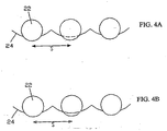
- Figures 4A and 4B show the semiconductor elements mounted in a perforated foil of the optical concentrators of Figure 2 ;
- Figure 5A shows one of the semiconductor elements mounted in the perforated aluminum foil of Figure 4 , prior to exposure of the second side of the p-n junction;
- Figure 5B shows the semiconductor element of Figure 5A , with the second side of the p-n junction exposed.
- a method of fabricating a photovoltaic solar cell according to a first embodiment of the present invention will now be described.
- a plurality of generally spherical semiconductor elements are used.
- Each of the semiconductor elements has a core and an outer surface of a layer of doped silicon forming a p-n junction below the layer of doped silicon.
- An anti-reflection coating is deposited on the outer surface of each of the semiconductor elements and the semiconductor elements are bonded into a perforated aluminum foil array, thereby providing ohmic contact to a first side of the p-n junction.
- the anti-reflection coating is then removed from a portion of each of the semiconductor elements in the array and then the core is exposed, thereby allowing ohmic contact to be made to a second side of the p-n junction.
- each of the semiconductor elements has a core and an outer surface forming a p-n junction below the outer surface.
- the semiconductor elements are coated with a titanium dioxide anti-reflection coating by chemical vapor deposition (CVD) of the titanium dioxide on the outer surface of the semiconductor elements within a CVD reactor.
- CVD chemical vapor deposition
- Decomposition of source vapors of titanium isopropoxide by reaction with oxygen, at elevated temperature, near the surface of the semiconductor elements results in the deposition of titanium dioxide (TiO 2 ).
- the oxygen source is introduced above the semiconductor elements.
- the nozzle that introduces the titanium isopropoxide to the CVD reactor is heated to a temperature of from about 100°C to about 175°C and preferably to about 150°C, to increase the gas temperature to a temperature near the reaction temperature.
- the semiconductor elements are also heated to a temperature in the range of about 200°C to about 500°C, and preferably to about 250°C, to aid in decomposition of the titanium isopropoxide.
- the semiconductor elements are continuously moved through the deposition area during deposition in order to provide a generally uniform coating of desired thickness.
- a vibratory tray 10 is employed to continuously move the semiconductor elements through the deposition zone.
- a tray vibrator drive 12 is attached to a tray and a heating mantle 14 is provided for preheating the semiconductor elements.
- the desired thickness and uniformity of the coating is achieved by multiple passes of the semiconductor elements through the vibratory tray 10.
- a generally uniform coating thickness of about 600 to about 900 angstroms is desirable and is achieved by passing the semiconductor elements through the vibratory tray 10 about three times to deposit from about 200 angstroms to about 300 angstroms of titanium dioxide per pass.
- a titanium dioxide coating thickness of about 600 to about 800 angstroms provides a dark blue coating of 1 ⁇ 4 wavelength for good anti-reflection performance.
- Appendix A includes a table showing the thickness of titanium dioxide anti-reflection coating and the resulting colours effected.
- FIGS. 2 and 3 show a top view and a perspective view, respectively, of the array of semiconductor elements in a periodic hexagonal array of optical concentrators.
- the coated semiconductor elements 22 are bonded into the periodic hexagonal array of optical concentrators made of a perforated aluminum foil 24.
- the aluminum foil 24 has a thickness of about 0.075 mm (0.003 inches) to about 0.125 mm (0.005 inches).
- the hexagonal periodic array of optical concentrators is a hexagonal or honeycomb structure of a plurality of substantially spherical depressions in the aluminum foil 24. Each spherical depression has a radius of curvature R of, for example, 0.915mm (0.036 inches).
- the aluminum foil 24 includes perforations or apertures for receiving the spherical semiconductor elements 22.
- the spacing S of the spherical semiconductor elements 22 is dependent on the spacing of the apertures in the aluminum foil 24.
- each spherical semiconductor element 22 has a diameter D in the range of about 0.3 mm to about 0.9 mm and preferably in the range of about 0.6 mm (0.024 inches) to about 0.8 mm (0.032 inches).
- Each spherical semiconductor element 22 in a single cell has a similar nominal diameter.
- the spherical semiconductor elements 22 are mounted in the spherical depressions of the perforated aluminum foil 24, resulting in a spherical element spacing of S, as shown.
- Figures 4A and 4B show the mounting of the spherical semiconductor elements 22 in the perforated aluminum foil 24.
- the spherical semiconductor elements 22 are loaded into the perforations in the aluminum foil 24.
- the elements 22 are bonded at a temperature less than the eutectic temperature for aluminum silicide formation (less than about 577°C), and preferably in the range of about 540°C to about 555°C, and a rolling mill force in the range of about 2500lbs (1134 Kg) to about 3500 lbs force (1588 Kg) for each 10mm of cell width, thereby dissolving the anti-reflection coating at a bond line of the semiconductor element 22 and the aluminum foil 24.
- an aluminum-silicon bond is formed between the foil 24 and the semiconductor element 22 to provide ohmic contact to the first side of the p-n junction.
- FIG. 5A shows one of the semiconductor elements 22 mounted in the perforated aluminum foil 24, prior to exposure of the second side of the p-n junction.
- the anti-reflective coating is then removed from the backside of each of the semiconductor elements 22 by chemical etching.
- the backside of each of the semiconductor elements 22 is exposed to concentrated hydrofluoric acid by spraying the backside of each of the semiconductor elements with concentrated hydrofluoric acid to etch away the TiO 2 .
- the backside is immersed in hydrofluoric acid or a paste with hydrofluoric acid and an inert carrier is applied to the backside.
- the backside of each of the semiconductor elements is etched with a mixture of hydrofluoric acid and nitric acid to etch away the doped silicon layer of the semiconductor elements, as shown in Figure 5B , and thereby allow for ohmic contact to be made to the second side of the p-n junction.
- the aluminum foil 24 serves as an etch mask during etching of the backside of the semiconductor elements 22.
- the backside of each of the semiconductor elements is etched with a caustic etchant such as NaOH, KOH, NH 4 OH, etc, to etch away the doped silicon layer.
- the semiconductor elements are loaded into a porous rotating drum rather than passing through a vibratory tray 10, for continuous movement to provide a generally uniform coating of desired thickness.
- the source vapours, titanium isopropoxide, an oxygen source, and nitrogen are decomposed in the drum.
- the porous rotating drum is used for batch processing.
- the porous rotating drum is slightly tilted such that the semiconductor elements gradually pass through the drum due to gravity. It will be appreciated that this process is continuous rather than a batch process.
- the semiconductor elements are continuously moved in a fluidized bed.
- the source vapours, titanium isopropoxide, the oxygen source, and nitrogen carrier gas are flowed through the bed to cause decomposition of the titanium isopropoxide in the bulk of the semiconductor elements.
- the fluidized bed is modified for continuous processing of semiconductor elements, rather than batch processing.
- the semiconductor elements are coated with a silicon nitride (Si 3 N 4 ) anti-reflection coating by reactive gas decomposition, known as plasma enhanced chemical vapor deposition.
- silane (SiH 4 ) or fluoro or chloro silane, is reacted with nitrogen or nitrogen containing gas, such as ammonia.
- Nitrogen plasma is used to catalyze the decomposition.
- the semiconductor elements are continuously moved during coating, and similar techniques to those already described in the first embodiment and the variation described above, can be employed to continuously move the elements. As described hereinabove, different colours can be effected by varying the thickness of the anti-reflection coating, thereby varying the wavelength.
- the thickness of silicon nitride coating is determined by multiplying the given thickness for titanium dioxide, by 1.364.
- the semiconductor elements are then mounted in the aluminum foil, in a similar manner to that described above.
- the backside of each of the semiconductor elements is subjected to mechanical or chemical-mechanical polishing. This process results in the removal of the anti-reflection coating along with the doped layer of silicon on the backside of each semiconductor element.
- the semiconductor elements are continuously moved by packing the elements into a column and continuously removing semiconductor elements from the bottom of the column while feeding semiconductor elements to the top.
- the source vapours, titanium isopropoxide, the oxygen source, and nitrogen are decomposed in the column.
- the semiconductor elements are sputter coated to form a titanium dioxide anti-reflection coating.
- a sputtering target is employed to create a metal coating on the surfaces of the semiconductor elements and the surfaces are subsequently oxidized.
- titanium dioxide is directly deposited on the surface of the semiconductor elements. This is accomplished using either a titanium dioxide target or a titanium target that is oxidized on the surface.
- the semiconductor elements are continuously moved during coating. It will be understood, however, that sputtering is performed in a vacuum to produce an anti-reflection coating and therefore the use of a fluidized bed is not suitable in the present embodiment. Other continuous movement techniques can be employed, however.
- the semiconductor elements are continuously moved using a rotating disk.
- the elements are introduced to the disk and rotate through almost 360 degrees.
- the elements are then swept off into a collection area.
- the semiconductor elements are coated using a modified sol-gel process.
- a small amount of gel solution of hydrolized metal alkoxide suspended in a solvent carrier is added to a plurality of semiconductor elements.
- the semiconductor elements are continually stirred to distribute the solution uniformly over the surfaces of the plurality of semiconductor elements and to evaporate the solvent.
- suitable mixers including vibratory bowl de-burring machines, tumble mixers, and ball mills, for example.
- the aluminum foil 24 is surface treated to improve reflectivity of the aluminum foil 24.
- reflectivity As will be understood by those skilled in the art, light in the 400nm to 1100nm range is of particular interest, since this range includes most of the solar spectrum. Aluminum reflectivity is generally very good in this range except for a slight decrease in reflectivity in the 700nm to 900nm range.
- the aluminum foil 24 is surface treated to improve reflectivity. For example, prior to bonding the coated semiconductor elements 22 into the aluminum foil 24, the aluminum foil 24 is mechanically polished by known means such as mechanical buffing, brushing, and burnishing, to smooth out irregularities in the surface of the aluminum foil 24 and to thereby improve reflectivity.
- the mechanical polishing is carried out using a polish (with a fine grit) that leaves a microscopically smooth surface with microscopically fine scratches to increase reflectivity of the aluminum foil 24.
- the above surface treatments for improving reflectivity of the aluminum foil 24 are carried out prior to forming the perforated-aluminum foil array 24 and thus, prior to bonding the coated semiconductor elements 22 into the aluminum foil 24.
- the surface treatments for improving reflectivity of the aluminum foil 24 are carried out after forming the perforated aluminum foil array 24 and prior to bonding the coated semiconductor elements 22 into the aluminum foil.
- an anti-reflection coating of silicon dioxide can be employed. Similar colours to those in Appendix A for titanium dioxide, can be effected for the silicon dioxide anti-reflection coating. To effect the same colours, the thickness of silicon dioxide coating is determined by multiplying the given thickness for titanium dioxide, by 1.82. Still other modifications and variations are possible. All such modifications and variations are believed to be within the scope and sphere of the present invention.
- FILM THICKNESS (microns) COLOR & COMMENTS 0.028 Tan 0.041 Brown 0.055 Dark violet to red-violet 0.069 Royal blue 0.083 Light blue to metallic blue 0.096 Metallic to very light yellow-green 0.110 Light gold or yellow - slightly metallic Gold with slight yellow-orange 0.124 Orange to melon 0.138 Red-violet 0.151 0.165 Blue to violet-blue 0.171 Blue 0.179 Blue to blue-green 0.190 Light green 0.193 Green to yellow-green 0.201 Yellow-green 0.206 Green-yellow 0.215 Yellow
Landscapes
- Photovoltaic Devices (AREA)
- Chemical Vapour Deposition (AREA)
Claims (17)
- Verfahren zur Herstellung eines optischen Konzentrators für eine photovoltaische Solarzelle, umfassend:Bereitstellen einer Aluminiumfolie (24), die eine Anordnung von perforierten, im Wesentlichen kugelartigen Vertiefungen aufweist;Bereitstellen einer Vielzahl von im Allgemeinen kugelartigen Halbleiterelementen (22), wobei jedes der Halbleiterelemente (22) einen Kern und eine Außenfläche hat, wobei eines, nämlich der Kern oder die Außenfläche aus p-Typ-Halbleitermaterial ausgebildet ist und das andere, nämlich der Kern bzw. die Außenfläche aus n-Typ-Halbleitermaterial ausgebildet ist, um dadurch einen pn-Übergang zu bilden;Aufbringen einer Antireflexbeschichtung auf die Außenfläche jedes der Halbleiterelemente (22);Einbringen jedes beschichteten Halbleiterelements (22) in eine jeweilige der Vertiefungen und Verbinden jedes Halbleiterelements (22) mit der Aluminiumfolie (24), wodurch ohmscher Kontakt zwischen der Außenfläche jedes Halbleiterelements (22) und der Aluminiumfolie (24) hergestellt werden kann; undEntfernen der Antireflexbeschichtung und der Außenfläche von einem Abschnitt der Rückseite des Halbleiterelements (22) bei jedem Halbleiterelement (22), um dadurch den Kern freizulegen und zuzulassen, dass der ohmsche Kontakt mit dem Kern hergestellt wird.
- Verfahren zur Herstellung eines optischen Konzentrators für eine photovoltaische Solarzelle nach Anspruch 1, wobei das Aufbringen einer Antireflexbeschichtung umfasst: Aufbringen eines Metalloxids auf die Außenfläche jedes der Halbleiterelemente (22).
- Verfahren zur Herstellung eines optischen Konzentrators für eine photovoltaische Solarzelle nach Anspruch 2, wobei das Aufbringen eines Metalloxids umfasst: Aufbringen von Titandioxid auf die Außenfläche jedes der Halbleiterelemente (22).
- Verfahren zur Herstellung eines optischen Konzentrators für eine photovoltaische Solarzelle nach Anspruch 1, wobei das Aufbringen einer Antireflexbeschichtung umfasst: Aufbringen einer Nichtoxidzusammensetzung auf die Außenfläche jedes der Halbleiterelemente (22).
- Verfahren zur Herstellung eines optischen Konzentrators für eine photovoltaische Solarzelle nach Anspruch 4, wobei das Aufbringen einer Nichtoxidzusammensetzung umfasst: Aufbringen von Siliciumnitrid auf die Außenfläche jedes der Halbleiterelemente (22).
- Verfahren zur Herstellung eines optischen Konzentrators für eine photovoltaische Solarzelle nach Anspruch 1, wobei das Verbinden umfasst: Thermokompressionsbonden jedes der Halbleiterelemente (22) mit der perforierten Aluminiumfolie (24), Auflösen der Antireflexbeschichtung an einer Haftschicht jedes der Halbleiterelemente (22) und Ausbilden einer Aluminium-Silicium-Verbindung zwischen der Aluminiumfolie (24) und jedem der Halbleiterelemente (22).
- Verfahren zur Herstellung eines optischen Konzentrators für eine photovoltaische Solarzelle nach Anspruch 6, wobei das Verbinden umfasst: Thermokompressionsbonden jedes der Halbleiterelemente (22) mit der perforierten Aluminiumfolie (24) bei einer Temperatur kleiner als die eutektische Temperatur für die Aluminiumsilicidbildung.
- Verfahren zur Herstellung eines optischen Konzentrators für eine photovoltaische Solarzelle nach Anspruch 1, wobei das Entfernen der Antireflexbeschichtung umfasst: Einwirkenlassen von Flusssäure auf den Abschnitt jedes der Halbleiterelemente (22).
- Verfahren zur Herstellung eines optischen Konzentrators für eine photovoltaische Solarzelle nach Anspruch 1, wobei das Entfernen der Antireflexbeschichtung umfasst: mechanisches Polieren und chemisch-mechanisches Polieren.
- Verfahren zur Herstellung einer optischen Konzentrators für eine photovoltaische Solarzelle nach Anspruch 1, wobei das Aufbringen der Antireflexbeschichtung auf die Außenfläche jedes der Halbleiterelemente (22) ferner umfasst: kontinuierliches Bewegen der Elemente durch mindestens eines von Folgendem: Vibrierenlassen in Schalen (10), Bewegen in Vibrationstrommeln, Bewegen in Trommeln, Wirbelschichtbehandlung, mechanisches Rühren und eine Kombination daraus, um eine im Wesentlichen gleichmäßige Antireflexbeschichtungsdicke von etwa 600 bis etwa 900 Angström aufzubringen.
- Verfahren zur Herstellung eines optischen Konzentrators für eine photovoltaische Solarzelle nach Anspruch 1, wobei das Aufbringen der Antireflexbeschichtung auf die Außenfläche jedes der Halbleiterelemente (22) ferner umfasst: Packen der Halbleiterelemente (22) in eine Kolonne und Einleiten von Quellgasen in die Kolonne, um eine im Wesentlichen gleichmäßige Antireflexbeschichtungsdicke von etwa 600 bis etwa 900 Angström aufzubringen.
- Verfahren zur Herstellung eines optischen Konzentrators für eine photovoltaische Solarzelle nach Anspruch 1, wobei das Entfernen mindestens eines von Folgendem umfasst: Einwirkenlassen eines Gemischs aus Flusssäure und Salpetersäure auf den Abschnitt jedes der Halbleiterelemente (22), Einwirkenlassen eines kaustischen Ätzmittels auf den Abschnitts jedes der Halbleiterelemente (22), mechanisches Polieren des Abschnitts jedes der Halbleiterelemente (22) und chemisch-mechanisches Polieren des Abschnitts jedes der Halbleiterelemente (22).
- Verfahren zur Herstellung eines optischen Konzentrators für eine photovoltaische Solarzelle nach Anspruch 2, wobei das Aufbringen umfasst: Aufbringen einer Metallbeschichtung durch Zerstäubung von einem Target mit anschließender Oxidation der Metallschicht.
- Verfahren zur Herstellung eines optischen Konzentrators für eine photovoltaische Solarzelle nach Anspruch 2, wobei das Abscheiden umfasst: Hydrolysieren eines Metallalkoxids in einem Sol-Gel-Prozess und Kondensieren des Metallalkoxids auf der Außenfläche jedes der Halbleiterelemente (22) bei kontinuierlicher Bewegung.
- Verfahren zur Herstellung eines optischen Konzentrators für eine photovoltaische Solarzellen gemäß Anspruch 1, wobei das Bereitstellen einer Aluminiumfolie (24) umfasst: Bereitstellen einer Aluminiumfolie (24) mit einer hexagonalen Anordnung der im Wesentlichen kugelartigen, perforierten Vertiefungen.
- Verfahren zur Herstellung eines optischen Konzentrators für eine photovoltaische Solarzelle nach Anspruch 15, wobei das Verbinden umfasst: Thermokompressionsbonden jedes der Halbleiterelemente (22) mit der perforierten Aluminiumfolie (24), Auflösen der Antireflexbeschichtung an einer Haftschicht jedes der Halbleiterelemente (22) und Ausbilden einer Aluminium-Silicium-Verbindung zwischen der Aluminiumfolie (24) und jedem der Halbleiterelemente (22).
- Verfahren zur Herstellung eines optischen Konzentrators für eine photovoltaische Solarzellen gemäß Anspruch 1 oder 15, ferner umfassend: Oberflächenbehandlung der Aluminiumfolie (24) zur Erhöhung des Reflexionsvermögens vor dem Verbinden jedes der Halbleiterelemente (22) mit der perforierten Aluminiumfolie (24).
Applications Claiming Priority (3)
| Application Number | Priority Date | Filing Date | Title |
|---|---|---|---|
| US10/348,253 US6897085B2 (en) | 2003-01-21 | 2003-01-21 | Method of fabricating an optical concentrator for a photovoltaic solar cell |
| US348253 | 2003-01-21 | ||
| PCT/CA2004/000187 WO2004066399A1 (en) | 2003-01-21 | 2004-01-21 | Method of fabricating an array of spherical solar cells |
Publications (2)
| Publication Number | Publication Date |
|---|---|
| EP1586121A1 EP1586121A1 (de) | 2005-10-19 |
| EP1586121B1 true EP1586121B1 (de) | 2012-05-02 |
Family
ID=32712516
Family Applications (1)
| Application Number | Title | Priority Date | Filing Date |
|---|---|---|---|
| EP04703739A Expired - Lifetime EP1586121B1 (de) | 2003-01-21 | 2004-01-21 | Verfahren zur herstellung eines arrays sphärischer solarzellen |
Country Status (8)
| Country | Link |
|---|---|
| US (2) | US6897085B2 (de) |
| EP (1) | EP1586121B1 (de) |
| JP (1) | JP5160781B2 (de) |
| CN (1) | CN1751397B (de) |
| AT (1) | ATE556437T1 (de) |
| AU (2) | AU2004205946A1 (de) |
| CA (1) | CA2513946C (de) |
| WO (1) | WO2004066399A1 (de) |
Families Citing this family (19)
| Publication number | Priority date | Publication date | Assignee | Title |
|---|---|---|---|---|
| US6897085B2 (en) * | 2003-01-21 | 2005-05-24 | Spheral Solar Power, Inc. | Method of fabricating an optical concentrator for a photovoltaic solar cell |
| JP2005317667A (ja) * | 2004-04-27 | 2005-11-10 | Clean Venture 21:Kk | 太陽電池用支持体およびその製造方法 |
| US7927933B2 (en) * | 2005-02-16 | 2011-04-19 | Imec | Method to enhance the initiation of film growth |
| ATE510306T1 (de) * | 2005-02-18 | 2011-06-15 | Clean Venture 21 Corp | Matrixanordnung sphärischer solarzellen und ihr herstellungsverfahren |
| JP4963199B2 (ja) * | 2006-07-28 | 2012-06-27 | 株式会社クリーンベンチャー21 | 光電変換装置の製造方法 |
| KR100821524B1 (ko) * | 2006-10-24 | 2008-04-14 | 한국과학기술연구원 | 염료 감응 태양전지용 산화물 전극의 제조방법 및 이를이용한 염료 감응 태양전지 |
| US8450594B2 (en) * | 2007-07-26 | 2013-05-28 | Guardian Industries Corp. | Method of making an antireflective silica coating, resulting product and photovoltaic device comprising same |
| US8445774B2 (en) * | 2007-07-26 | 2013-05-21 | Guardian Industries Corp. | Method of making an antireflective silica coating, resulting product, and photovoltaic device comprising same |
| US20100206370A1 (en) * | 2009-02-18 | 2010-08-19 | Qualcomm Incorporated | Photovoltaic Cell Efficiency Using Through Silicon Vias |
| US8617641B2 (en) * | 2009-11-12 | 2013-12-31 | Guardian Industries Corp. | Coated article comprising colloidal silica inclusive anti-reflective coating, and method of making the same |
| WO2012164767A1 (ja) * | 2011-05-27 | 2012-12-06 | 株式会社島津製作所 | 成膜装置及び成膜方法 |
| KR101336075B1 (ko) * | 2012-02-10 | 2013-12-03 | 최대규 | 소재의 가공장치 |
| US9394604B2 (en) * | 2012-04-16 | 2016-07-19 | The United States Of America As Represented By The Secretary Of The Army | Apparatus and method for sputter-deposited coatings on fluidized particle beds |
| KR101325572B1 (ko) * | 2012-05-09 | 2013-11-05 | 이성규 | Pcb를 이용한 태양전지 |
| JP6353636B2 (ja) * | 2013-06-21 | 2018-07-04 | 東京エレクトロン株式会社 | 酸化チタン膜の除去方法および除去装置 |
| US9666733B2 (en) | 2013-09-04 | 2017-05-30 | Hyeon Woo AHN | Solar cell using printed circuit board |
| US9818903B2 (en) * | 2014-04-30 | 2017-11-14 | Sunpower Corporation | Bonds for solar cell metallization |
| CN105140321B (zh) * | 2015-07-06 | 2017-02-01 | 南京汇金锦元光电材料有限公司 | 柔性cigs太阳能电池及其金属基底制备方法 |
| US10432137B2 (en) | 2017-09-25 | 2019-10-01 | Cameron Ernest Jabara | Solar energy collector and method of operation |
Family Cites Families (28)
| Publication number | Priority date | Publication date | Assignee | Title |
|---|---|---|---|---|
| US294723A (en) * | 1884-03-04 | New toek | ||
| US3025335A (en) * | 1960-02-29 | 1962-03-13 | Hoffman Electronics Corp | Flexible solar energy converter panel |
| US4361598A (en) * | 1979-08-10 | 1982-11-30 | Westinghouse Electric Corp. | Polymerized solutions for depositing optical oxide coatings |
| US4610077A (en) * | 1984-04-30 | 1986-09-09 | Hughes Aircraft Company | Process for fabricating a wraparound contact solar cell |
| US4957601A (en) * | 1984-09-04 | 1990-09-18 | Texas Instruments Incorporated | Method of forming an array of apertures in an aluminum foil |
| CN1012311B (zh) * | 1986-02-15 | 1991-04-03 | 德克萨斯仪器股份有限公司 | 制造太阳能电池阵列的方法 |
| US5698451A (en) * | 1988-06-10 | 1997-12-16 | Mobil Solar Energy Corporation | Method of fabricating contacts for solar cells |
| US4909856A (en) * | 1988-08-22 | 1990-03-20 | Hughes Aircraft Company | Composite coverglass for solar cell |
| US5081069A (en) * | 1989-12-26 | 1992-01-14 | Texas Instruments Incorporated | Method for depositing a Tio2 layer using a periodic and simultaneous tilting and rotating platform motion |
| US5360491A (en) * | 1993-04-07 | 1994-11-01 | The United States Of America As Represented By The United States Department Of Energy | β-silicon carbide protective coating and method for fabricating same |
| US5482568A (en) * | 1994-06-28 | 1996-01-09 | Hockaday; Robert G. | Micro mirror photovoltaic cells |
| US5498576A (en) * | 1994-07-22 | 1996-03-12 | Texas Instruments Incorporated | Method and apparatus for affixing spheres to a foil matrix |
| US5486494A (en) * | 1994-07-22 | 1996-01-23 | Texas Instruments Incorporated | Method and apparatus for affixing spheres to a conductive sheet |
| JPH08125210A (ja) * | 1994-10-24 | 1996-05-17 | Jiyousuke Nakada | 受光素子及び受光素子アレイ並びにそれらを用いた電解装置 |
| DE69637769D1 (de) * | 1996-10-09 | 2009-01-15 | Josuke Nakata | Halbleitervorrichtung |
| DE69725601T2 (de) * | 1997-08-27 | 2004-04-15 | Nakata, Josuke, Joyo | Sphärische halbleiteranordnung, verfahren zu seiner herstellung und sphärisches halbleiteranordnungmaterial |
| EP0982780B1 (de) * | 1998-01-23 | 2003-09-24 | Josuke Nakata | Vorrichtung zur optischen elektrolyse |
| JP3174549B2 (ja) | 1998-02-26 | 2001-06-11 | 株式会社日立製作所 | 太陽光発電装置及び太陽光発電モジュール並びに太陽光発電システムの設置方法 |
| US6156967A (en) * | 1998-06-04 | 2000-12-05 | Tecstar Power Systems, Inc. | Modular glass covered solar cell array |
| US6188012B1 (en) * | 1999-11-10 | 2001-02-13 | Tecstar Power Systems | Methods and systems for a solar cell concentrator |
| JP2001210843A (ja) * | 1999-11-17 | 2001-08-03 | Fuji Mach Mfg Co Ltd | 光発電パネルおよびその製造方法 |
| JP3992126B2 (ja) | 1999-12-16 | 2007-10-17 | 株式会社三井ハイテック | 太陽電池の製造方法 |
| JP3849907B2 (ja) * | 1999-12-24 | 2006-11-22 | 株式会社三井ハイテック | 太陽電池およびその製造方法 |
| US6355873B1 (en) * | 2000-06-21 | 2002-03-12 | Ball Semiconductor, Inc. | Spherical shaped solar cell fabrication and panel assembly |
| US6329296B1 (en) * | 2000-08-09 | 2001-12-11 | Sandia Corporation | Metal catalyst technique for texturing silicon solar cells |
| EP1255303B1 (de) | 2000-10-20 | 2016-06-29 | Sphelar Power Corporation | Lichtemittierendes oder lichtempfindliches halbleitermodul und seine herstellungsmethode |
| US6706959B2 (en) | 2000-11-24 | 2004-03-16 | Clean Venture 21 Corporation | Photovoltaic apparatus and mass-producing apparatus for mass-producing spherical semiconductor particles |
| US6897085B2 (en) * | 2003-01-21 | 2005-05-24 | Spheral Solar Power, Inc. | Method of fabricating an optical concentrator for a photovoltaic solar cell |
-
2003
- 2003-01-21 US US10/348,253 patent/US6897085B2/en not_active Expired - Lifetime
-
2004
- 2004-01-21 EP EP04703739A patent/EP1586121B1/de not_active Expired - Lifetime
- 2004-01-21 WO PCT/CA2004/000187 patent/WO2004066399A1/en not_active Ceased
- 2004-01-21 JP JP2006500444A patent/JP5160781B2/ja not_active Expired - Fee Related
- 2004-01-21 CA CA2513946A patent/CA2513946C/en not_active Expired - Fee Related
- 2004-01-21 CN CN200480004618XA patent/CN1751397B/zh not_active Expired - Fee Related
- 2004-01-21 AT AT04703739T patent/ATE556437T1/de active
- 2004-01-21 AU AU2004205946A patent/AU2004205946A1/en not_active Abandoned
-
2005
- 2005-05-23 US US11/135,080 patent/US7312097B2/en not_active Expired - Fee Related
-
2010
- 2010-04-01 AU AU2010201311A patent/AU2010201311B2/en not_active Ceased
Also Published As
| Publication number | Publication date |
|---|---|
| CA2513946C (en) | 2013-01-15 |
| CA2513946A1 (en) | 2004-08-05 |
| JP2006515717A (ja) | 2006-06-01 |
| US20040140001A1 (en) | 2004-07-22 |
| JP5160781B2 (ja) | 2013-03-13 |
| US20050217721A1 (en) | 2005-10-06 |
| CN1751397A (zh) | 2006-03-22 |
| AU2004205946A1 (en) | 2004-08-05 |
| ATE556437T1 (de) | 2012-05-15 |
| US6897085B2 (en) | 2005-05-24 |
| EP1586121A1 (de) | 2005-10-19 |
| AU2010201311A1 (en) | 2010-04-22 |
| AU2010201311B2 (en) | 2011-08-11 |
| US7312097B2 (en) | 2007-12-25 |
| WO2004066399A1 (en) | 2004-08-05 |
| CN1751397B (zh) | 2011-05-18 |
Similar Documents
| Publication | Publication Date | Title |
|---|---|---|
| AU2010201311B2 (en) | Method of fabricating an array of spherical solar cells | |
| US8227881B2 (en) | Solar cell and its method of manufacture | |
| EP2471110B1 (de) | Solarzelle und verfahren zur herstellung einer derartigen solarzelle | |
| US20120125256A1 (en) | Apparatus and method for repeatedly fabricating thin film semiconductor substrates using a template | |
| CN103456804A (zh) | 在多晶硅上形成倒金字塔型多孔表面纳米织构的方法及制备短波增强型太阳电池的方法 | |
| TW201203592A (en) | Oxide nitride stack for backside reflector of solar cell | |
| TW201031011A (en) | Edge film removal process for thin film solar cell applications | |
| EP2181464A2 (de) | Solarzelle mit poröser struktur und herstellungsverfahren dafür | |
| EP2711989B1 (de) | Ätzzusammensetzung und verfahren zum ätzen eines siliziumwafers | |
| CN110299420A (zh) | 晶硅太阳能电池的减反射膜沉积方法 | |
| JP2006073832A (ja) | 太陽電池及びその製造方法 | |
| CN103718311A (zh) | 用于制造太阳能电池的方法以及太阳能电池 | |
| WO2004023567A2 (en) | Method of manufacturing a solar cell | |
| JPS62105485A (ja) | 半導体基体の製造方法 | |
| CN117153902A (zh) | 一种局部隧穿氧化钝化接触的TOPCon电池 | |
| KR101023144B1 (ko) | 전사법을 이용한 태양전지 및 그 제조방법 | |
| CN111009588A (zh) | 一种perc电池及其制备方法 | |
| TW201123490A (en) | Solar cell and method of fabricating the same | |
| JP2003303984A (ja) | 太陽電池の製造方法およびその方法により製造する太陽電池 | |
| JP2025515821A (ja) | 電荷蓄積構造および電荷蓄積構造を製造する方法 | |
| JP4239134B2 (ja) | 太陽電池用の誘電体分離ウェーハの製造方法 | |
| CN109887841A (zh) | 一种perc电池背面抛光工艺 | |
| JP2006351995A (ja) | 光電変換素子の製造方法 | |
| JP2006210385A (ja) | 太陽電池の製造方法 | |
| CN119342933B (zh) | Ibc太阳能电池的背面接触结构、ibc太阳能电池及制备方法 |
Legal Events
| Date | Code | Title | Description |
|---|---|---|---|
| PUAI | Public reference made under article 153(3) epc to a published international application that has entered the european phase |
Free format text: ORIGINAL CODE: 0009012 |
|
| 17P | Request for examination filed |
Effective date: 20050729 |
|
| AK | Designated contracting states |
Kind code of ref document: A1 Designated state(s): AT BE BG CH CY CZ DE DK EE ES FI FR GB GR HU IE IT LI LU MC NL PT RO SE SI SK TR |
|
| AX | Request for extension of the european patent |
Extension state: AL LT LV MK |
|
| DAX | Request for extension of the european patent (deleted) | ||
| RAP1 | Party data changed (applicant data changed or rights of an application transferred) |
Owner name: ATS AUTOMATION TOOLING SYSTEMS INC. |
|
| 17Q | First examination report despatched |
Effective date: 20100813 |
|
| GRAP | Despatch of communication of intention to grant a patent |
Free format text: ORIGINAL CODE: EPIDOSNIGR1 |
|
| GRAS | Grant fee paid |
Free format text: ORIGINAL CODE: EPIDOSNIGR3 |
|
| GRAA | (expected) grant |
Free format text: ORIGINAL CODE: 0009210 |
|
| AK | Designated contracting states |
Kind code of ref document: B1 Designated state(s): AT BE BG CH CY CZ DE DK EE ES FI FR GB GR HU IE IT LI LU MC NL PT RO SE SI SK TR |
|
| REG | Reference to a national code |
Ref country code: GB Ref legal event code: FG4D |
|
| REG | Reference to a national code |
Ref country code: CH Ref legal event code: EP Ref country code: AT Ref legal event code: REF Ref document number: 556437 Country of ref document: AT Kind code of ref document: T Effective date: 20120515 |
|
| REG | Reference to a national code |
Ref country code: IE Ref legal event code: FG4D |
|
| REG | Reference to a national code |
Ref country code: DE Ref legal event code: R096 Ref document number: 602004037596 Country of ref document: DE Effective date: 20120705 |
|
| REG | Reference to a national code |
Ref country code: NL Ref legal event code: VDEP Effective date: 20120502 |
|
| PG25 | Lapsed in a contracting state [announced via postgrant information from national office to epo] |
Ref country code: CY Free format text: LAPSE BECAUSE OF FAILURE TO SUBMIT A TRANSLATION OF THE DESCRIPTION OR TO PAY THE FEE WITHIN THE PRESCRIBED TIME-LIMIT Effective date: 20120502 Ref country code: FI Free format text: LAPSE BECAUSE OF FAILURE TO SUBMIT A TRANSLATION OF THE DESCRIPTION OR TO PAY THE FEE WITHIN THE PRESCRIBED TIME-LIMIT Effective date: 20120502 Ref country code: SE Free format text: LAPSE BECAUSE OF FAILURE TO SUBMIT A TRANSLATION OF THE DESCRIPTION OR TO PAY THE FEE WITHIN THE PRESCRIBED TIME-LIMIT Effective date: 20120502 |
|
| REG | Reference to a national code |
Ref country code: AT Ref legal event code: MK05 Ref document number: 556437 Country of ref document: AT Kind code of ref document: T Effective date: 20120502 |
|
| PG25 | Lapsed in a contracting state [announced via postgrant information from national office to epo] |
Ref country code: GR Free format text: LAPSE BECAUSE OF FAILURE TO SUBMIT A TRANSLATION OF THE DESCRIPTION OR TO PAY THE FEE WITHIN THE PRESCRIBED TIME-LIMIT Effective date: 20120803 Ref country code: PT Free format text: LAPSE BECAUSE OF FAILURE TO SUBMIT A TRANSLATION OF THE DESCRIPTION OR TO PAY THE FEE WITHIN THE PRESCRIBED TIME-LIMIT Effective date: 20120903 Ref country code: SI Free format text: LAPSE BECAUSE OF FAILURE TO SUBMIT A TRANSLATION OF THE DESCRIPTION OR TO PAY THE FEE WITHIN THE PRESCRIBED TIME-LIMIT Effective date: 20120502 |
|
| PG25 | Lapsed in a contracting state [announced via postgrant information from national office to epo] |
Ref country code: BE Free format text: LAPSE BECAUSE OF FAILURE TO SUBMIT A TRANSLATION OF THE DESCRIPTION OR TO PAY THE FEE WITHIN THE PRESCRIBED TIME-LIMIT Effective date: 20120502 |
|
| PG25 | Lapsed in a contracting state [announced via postgrant information from national office to epo] |
Ref country code: AT Free format text: LAPSE BECAUSE OF FAILURE TO SUBMIT A TRANSLATION OF THE DESCRIPTION OR TO PAY THE FEE WITHIN THE PRESCRIBED TIME-LIMIT Effective date: 20120502 Ref country code: SK Free format text: LAPSE BECAUSE OF FAILURE TO SUBMIT A TRANSLATION OF THE DESCRIPTION OR TO PAY THE FEE WITHIN THE PRESCRIBED TIME-LIMIT Effective date: 20120502 Ref country code: RO Free format text: LAPSE BECAUSE OF FAILURE TO SUBMIT A TRANSLATION OF THE DESCRIPTION OR TO PAY THE FEE WITHIN THE PRESCRIBED TIME-LIMIT Effective date: 20120502 Ref country code: EE Free format text: LAPSE BECAUSE OF FAILURE TO SUBMIT A TRANSLATION OF THE DESCRIPTION OR TO PAY THE FEE WITHIN THE PRESCRIBED TIME-LIMIT Effective date: 20120502 Ref country code: NL Free format text: LAPSE BECAUSE OF FAILURE TO SUBMIT A TRANSLATION OF THE DESCRIPTION OR TO PAY THE FEE WITHIN THE PRESCRIBED TIME-LIMIT Effective date: 20120502 Ref country code: DK Free format text: LAPSE BECAUSE OF FAILURE TO SUBMIT A TRANSLATION OF THE DESCRIPTION OR TO PAY THE FEE WITHIN THE PRESCRIBED TIME-LIMIT Effective date: 20120502 Ref country code: CZ Free format text: LAPSE BECAUSE OF FAILURE TO SUBMIT A TRANSLATION OF THE DESCRIPTION OR TO PAY THE FEE WITHIN THE PRESCRIBED TIME-LIMIT Effective date: 20120502 |
|
| PG25 | Lapsed in a contracting state [announced via postgrant information from national office to epo] |
Ref country code: IT Free format text: LAPSE BECAUSE OF FAILURE TO SUBMIT A TRANSLATION OF THE DESCRIPTION OR TO PAY THE FEE WITHIN THE PRESCRIBED TIME-LIMIT Effective date: 20120502 |
|
| PLBE | No opposition filed within time limit |
Free format text: ORIGINAL CODE: 0009261 |
|
| STAA | Information on the status of an ep patent application or granted ep patent |
Free format text: STATUS: NO OPPOSITION FILED WITHIN TIME LIMIT |
|
| 26N | No opposition filed |
Effective date: 20130205 |
|
| PG25 | Lapsed in a contracting state [announced via postgrant information from national office to epo] |
Ref country code: ES Free format text: LAPSE BECAUSE OF FAILURE TO SUBMIT A TRANSLATION OF THE DESCRIPTION OR TO PAY THE FEE WITHIN THE PRESCRIBED TIME-LIMIT Effective date: 20120813 |
|
| REG | Reference to a national code |
Ref country code: DE Ref legal event code: R097 Ref document number: 602004037596 Country of ref document: DE Effective date: 20130205 |
|
| PG25 | Lapsed in a contracting state [announced via postgrant information from national office to epo] |
Ref country code: BG Free format text: LAPSE BECAUSE OF FAILURE TO SUBMIT A TRANSLATION OF THE DESCRIPTION OR TO PAY THE FEE WITHIN THE PRESCRIBED TIME-LIMIT Effective date: 20120802 |
|
| PG25 | Lapsed in a contracting state [announced via postgrant information from national office to epo] |
Ref country code: MC Free format text: LAPSE BECAUSE OF NON-PAYMENT OF DUE FEES Effective date: 20130131 |
|
| REG | Reference to a national code |
Ref country code: CH Ref legal event code: PL |
|
| GBPC | Gb: european patent ceased through non-payment of renewal fee |
Effective date: 20130121 |
|
| REG | Reference to a national code |
Ref country code: IE Ref legal event code: MM4A |
|
| REG | Reference to a national code |
Ref country code: FR Ref legal event code: ST Effective date: 20130930 |
|
| PG25 | Lapsed in a contracting state [announced via postgrant information from national office to epo] |
Ref country code: LI Free format text: LAPSE BECAUSE OF NON-PAYMENT OF DUE FEES Effective date: 20130131 Ref country code: DE Free format text: LAPSE BECAUSE OF NON-PAYMENT OF DUE FEES Effective date: 20130801 Ref country code: CH Free format text: LAPSE BECAUSE OF NON-PAYMENT OF DUE FEES Effective date: 20130131 |
|
| REG | Reference to a national code |
Ref country code: DE Ref legal event code: R119 Ref document number: 602004037596 Country of ref document: DE Effective date: 20130801 |
|
| PG25 | Lapsed in a contracting state [announced via postgrant information from national office to epo] |
Ref country code: GB Free format text: LAPSE BECAUSE OF NON-PAYMENT OF DUE FEES Effective date: 20130121 Ref country code: FR Free format text: LAPSE BECAUSE OF NON-PAYMENT OF DUE FEES Effective date: 20130131 |
|
| PG25 | Lapsed in a contracting state [announced via postgrant information from national office to epo] |
Ref country code: IE Free format text: LAPSE BECAUSE OF NON-PAYMENT OF DUE FEES Effective date: 20130121 |
|
| PG25 | Lapsed in a contracting state [announced via postgrant information from national office to epo] |
Ref country code: TR Free format text: LAPSE BECAUSE OF FAILURE TO SUBMIT A TRANSLATION OF THE DESCRIPTION OR TO PAY THE FEE WITHIN THE PRESCRIBED TIME-LIMIT Effective date: 20120502 |
|
| PG25 | Lapsed in a contracting state [announced via postgrant information from national office to epo] |
Ref country code: LU Free format text: LAPSE BECAUSE OF NON-PAYMENT OF DUE FEES Effective date: 20130121 Ref country code: HU Free format text: LAPSE BECAUSE OF FAILURE TO SUBMIT A TRANSLATION OF THE DESCRIPTION OR TO PAY THE FEE WITHIN THE PRESCRIBED TIME-LIMIT; INVALID AB INITIO Effective date: 20040121 |