US5081069A - Method for depositing a Tio2 layer using a periodic and simultaneous tilting and rotating platform motion - Google Patents
Method for depositing a Tio2 layer using a periodic and simultaneous tilting and rotating platform motion Download PDFInfo
- Publication number
- US5081069A US5081069A US07/457,113 US45711389A US5081069A US 5081069 A US5081069 A US 5081069A US 45711389 A US45711389 A US 45711389A US 5081069 A US5081069 A US 5081069A
- Authority
- US
- United States
- Prior art keywords
- gas
- reaction chamber
- platform
- imparting
- titanium
- Prior art date
- Legal status (The legal status is an assumption and is not a legal conclusion. Google has not performed a legal analysis and makes no representation as to the accuracy of the status listed.)
- Expired - Lifetime
Links
Images

Classifications
-
- H—ELECTRICITY
- H10—SEMICONDUCTOR DEVICES; ELECTRIC SOLID-STATE DEVICES NOT OTHERWISE PROVIDED FOR
- H10F—INORGANIC SEMICONDUCTOR DEVICES SENSITIVE TO INFRARED RADIATION, LIGHT, ELECTROMAGNETIC RADIATION OF SHORTER WAVELENGTH OR CORPUSCULAR RADIATION
- H10F71/00—Manufacture or treatment of devices covered by this subclass
- H10F71/138—Manufacture of transparent electrodes, e.g. transparent conductive oxides [TCO] or indium tin oxide [ITO] electrodes
-
- C—CHEMISTRY; METALLURGY
- C23—COATING METALLIC MATERIAL; COATING MATERIAL WITH METALLIC MATERIAL; CHEMICAL SURFACE TREATMENT; DIFFUSION TREATMENT OF METALLIC MATERIAL; COATING BY VACUUM EVAPORATION, BY SPUTTERING, BY ION IMPLANTATION OR BY CHEMICAL VAPOUR DEPOSITION, IN GENERAL; INHIBITING CORROSION OF METALLIC MATERIAL OR INCRUSTATION IN GENERAL
- C23C—COATING METALLIC MATERIAL; COATING MATERIAL WITH METALLIC MATERIAL; SURFACE TREATMENT OF METALLIC MATERIAL BY DIFFUSION INTO THE SURFACE, BY CHEMICAL CONVERSION OR SUBSTITUTION; COATING BY VACUUM EVAPORATION, BY SPUTTERING, BY ION IMPLANTATION OR BY CHEMICAL VAPOUR DEPOSITION, IN GENERAL
- C23C16/00—Chemical coating by decomposition of gaseous compounds, without leaving reaction products of surface material in the coating, i.e. chemical vapour deposition [CVD] processes
- C23C16/22—Chemical coating by decomposition of gaseous compounds, without leaving reaction products of surface material in the coating, i.e. chemical vapour deposition [CVD] processes characterised by the deposition of inorganic material, other than metallic material
- C23C16/30—Deposition of compounds, mixtures or solid solutions, e.g. borides, carbides, nitrides
- C23C16/40—Oxides
- C23C16/405—Oxides of refractory metals or yttrium
-
- C—CHEMISTRY; METALLURGY
- C23—COATING METALLIC MATERIAL; COATING MATERIAL WITH METALLIC MATERIAL; CHEMICAL SURFACE TREATMENT; DIFFUSION TREATMENT OF METALLIC MATERIAL; COATING BY VACUUM EVAPORATION, BY SPUTTERING, BY ION IMPLANTATION OR BY CHEMICAL VAPOUR DEPOSITION, IN GENERAL; INHIBITING CORROSION OF METALLIC MATERIAL OR INCRUSTATION IN GENERAL
- C23C—COATING METALLIC MATERIAL; COATING MATERIAL WITH METALLIC MATERIAL; SURFACE TREATMENT OF METALLIC MATERIAL BY DIFFUSION INTO THE SURFACE, BY CHEMICAL CONVERSION OR SUBSTITUTION; COATING BY VACUUM EVAPORATION, BY SPUTTERING, BY ION IMPLANTATION OR BY CHEMICAL VAPOUR DEPOSITION, IN GENERAL
- C23C16/00—Chemical coating by decomposition of gaseous compounds, without leaving reaction products of surface material in the coating, i.e. chemical vapour deposition [CVD] processes
- C23C16/44—Chemical coating by decomposition of gaseous compounds, without leaving reaction products of surface material in the coating, i.e. chemical vapour deposition [CVD] processes characterised by the method of coating
- C23C16/458—Chemical coating by decomposition of gaseous compounds, without leaving reaction products of surface material in the coating, i.e. chemical vapour deposition [CVD] processes characterised by the method of coating characterised by the method used for supporting substrates in the reaction chamber
- C23C16/4582—Rigid and flat substrates, e.g. plates or discs
- C23C16/4587—Rigid and flat substrates, e.g. plates or discs the substrate being supported substantially vertically
- C23C16/4588—Rigid and flat substrates, e.g. plates or discs the substrate being supported substantially vertically the substrate being rotated
-
- Y—GENERAL TAGGING OF NEW TECHNOLOGICAL DEVELOPMENTS; GENERAL TAGGING OF CROSS-SECTIONAL TECHNOLOGIES SPANNING OVER SEVERAL SECTIONS OF THE IPC; TECHNICAL SUBJECTS COVERED BY FORMER USPC CROSS-REFERENCE ART COLLECTIONS [XRACs] AND DIGESTS
- Y02—TECHNOLOGIES OR APPLICATIONS FOR MITIGATION OR ADAPTATION AGAINST CLIMATE CHANGE
- Y02E—REDUCTION OF GREENHOUSE GAS [GHG] EMISSIONS, RELATED TO ENERGY GENERATION, TRANSMISSION OR DISTRIBUTION
- Y02E10/00—Energy generation through renewable energy sources
- Y02E10/50—Photovoltaic [PV] energy
Definitions
- This invention relates in general to the deposition of a layer of material on the surface of an object, and more particularly to a method and apparatus for depositing a layer on a spherical object.
- a titanium containing solution is spun onto a flat surface to form a thin layer of titanium dioxide to serve as the anti-reflective layer.
- uniform coverage and thickness on the hemispherical surfaces of the silicon cells is difficult to obtain.
- a titanium metal is sputtered onto the desired surface and then oxidized to form titanium dioxide.
- oxidation of the metal requires high temperatures which may damage or destroy the material of the solar array.
- Depositing layers by CVD methods on spherical surfaces also does not result in uniform thickness and coverage when applied to irregular or curved surfaces, such as the hemispherical surfaces of the spherical solar cells.
- Such deposition is anisotropic such that only those areas of the solar cell surface which are approximately perpendicular to the flow of the reacting chemicals obtain an adequate layer.
- Other areas of the surface, such as those on the sides of the silicon spheres, are approximately parallel to the flow of the reacting chemicals and obtain an inadequate deposit.
- an apparatus and method are provided which substantially eliminate the disadvantages and problems associated with prior methods of depositing a layer of material, such as titanium dioxide, on the surface of spherical objects.
- a mixing chamber is provided to allow a first set of gases to mix, such as titanium isoproxide (TIP) vapor and oxygen.
- a first set of gases such as titanium isoproxide (TIP) vapor and oxygen.
- the mixture of the first gases is injected into a reaction chamber as is a second gas, such as water vapor.
- a second gas such as water vapor.
- the object in the reaction chamber is attached to a platform which is simultaneously and periodically tilted and rotated.
- a platform which is simultaneously and periodically tilted and rotated.
- the apparatus and method of the present invention provide the technical advantage of depositing a uniform layer of material on the surface of an object, including, but not limited to, surfaces which are spherical.
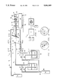
- FIG. 1 illustrates a block diagram of the present invention
- FIG. 2 illustrates a detailed schematic representation of the present invention
- FIG. 3 illustrates a sectional view of the barrier wall between the mixing and reaction chambers on the line II--II in FIG. 2;
- FIG. 4 illustrates a sectional view of the end wall of the mixing chamber on the line III--III in FIG. 2;
- FIG. 5 illustrates a detailed view of the solar array platform held by the rotation tube and push rod
- FIG. 6 illustrates a detailed view of the drive mechanisms for tilting and rotating the platform
- FIG. 7 illustrates an alternative embodiment of the drive mechanisms.
- FIGS. 1-7 of the drawings like numerals being used for like and corresponding parts of the various drawings.
- FIG. 1 illustrates a block diagram of the apparatus of the present invention, indicated generally as 1.
- Two gas sources 2 and 3 are coupled to a mixing chamber 4.
- Mixing chamber 4 is coupled to a reaction chamber 5.
- a gas source 6 is also coupled to reaction chamber 5.
- a solar array 7, or other surface to be coated with a layer of material, is placed inside reaction chamber 5.
- gas sources 2 and 3 inject two gases into mixing chamber 4 where the gases mix to form a third gas which is injected into reaction chamber 5.
- Gas source 6 injects a fourth gas into reaction chamber 5 in the same direction as the third gas is injected.
- the third and fourth gases do not react instantaneously, but rather react at a known rate. Because of the injection velocities of the gases, the reaction is substantially completed at a location within reaction chamber 5 a calculated distance from the points at which the gases are injected.
- Solar array 7 is positioned in reaction chamber 5 at the calculated location such that the reaction is substantially completed at the surface of solar array 7.
- Solar array 7 is simultaneously tilted and rotated within reaction chamber 5 thereby exposing all areas of the surface of solar array 7 to the reacting gases. Consequently, the reactant, an antireflective material, is deposited in a uniform layer on the surface of solar array 7.
- the first and second gases are oxygen and titanium isoproxide vapor, respectively, and the third gas is a mixture of the two.
- the fourth gas is water vapor and the antireflective reactant is titanium dioxide.
- FIG. 2 shows more detailed a schematic representation of the apparatus of the present invention
- Mixing chamber 4 and reaction chamber 5 are placed end-to-end in a furnace 16 and are separated by a barrier wall 18.
- An end wall 20 of mixing chamber 4 seals mixing chamber 4 from the outside environment.
- Two holes 22 and 24 formed in end wall 20 serve as input ports to mixing chamber 4.
- An additional hole 26 formed in end wall 20 permits an inlet line 28 to pass through mixing chamber 4 and into reaction chamber 5.
- An injection port 30 formed in barrier wall 18 between the two chambers 4 and 5 allows the chemical mixture formed in mixing chamber 4 to pass into reaction chamber 5.
- inlet line 28 passes through injection port 30 into reaction chamber 5.
- Oxygen is supplied by gas source 2 through a valve 34 coupled to a tube 36.
- Tube 36 terminates at input port 22 in end wall 20 of mixing chamber 4.
- a titanium isoproxide (TIP) solution is held in a gas source 3 to be heated by a heater 40.
- One end of tube 42 is submerged in the TIP solution; the other end of tube 42 is connected to a valve 44 which is coupled to another tube 46 which terminates at nitrogen gas tank 48.
- One end of another tube 50 is situated above the TIP solution.
- the other end of tube 50 is coupled to tube 52 which terminates at input port 24 in end wall 20 of mixing chamber 4.
- Tube 52 is also coupled to nitrogen tube 46 through valve 54.
- a tube 56 is submerged in deionized water held in a gas source 6.
- Tube 56 is coupled to nitrogen tube 46 through valve 60.
- One end of another tube 62 is situated above the surface of the water.
- the other end of tube 62 is coupled to inlet line 28 which terminates in reaction chamber 5.
- Inlet line 28 is also coupled to nitrogen tube 46 through valve 64.
- Solar array 7 is clipped onto one side of platform 68.
- Platform 68 is coupled on the other side to rotation tube 70 with two pivots 72.
- Rotation tube 70 is held in place by bearing units 74 attached to base 76.
- a cog-belt drive, indicated generally at 78, is placed circumferentially around rotation tube 70 and is coupled to a motor (not shown).
- Push rod 80 is also coupled to platform 68 with pivot 82.
- Push rod 80 is situated inside rotation tube 70 and the end opposite platform 68 is coupled to cam 84 with ball joint 86.
- Cam 84 is coupled to a shaft 88 of motor 90 which is attached to base 76.
- a set of wheels 92 attached to base 76 allow platform 68 and solar array 7 to be easily pushed into and pulled out of reaction chamber 5.
- FIG. 3 illustrates a view of barrier wall 18 between mixing chamber 4 and reaction chamber 5. Opening 30 is shown in the center of barrier wall 18 with tube 28 passing through opening 30.
- FIG. 4 illustrates a view of end wall 20 of mixing chamber 4 and shows the locations of injection ports 22 and 24 and opening 26 through which inlet line 28 passes.
- FIG. 5 illustrates the details of the pivots connecting platform 68 with rotation tube 70 and push rod 80.
- Solar array 7 is clipped to the side of platform 68 opposite the side shown in FIG. 5.
- Opposite sides of the end of rotation tube 70 have been cut away as indicated and pins 93 are inserted through attachment plates 94 and through holes (not shown) formed in the end of rotation tube 70.
- a similar pivot 82 provides the attachment for push rod 80 to platform 68.
- Push rod 80 is placed between two attachment plates 96 and pin 98 is inserted through holes formed in attachment plates 96 and push rod 80.
- Pivot 82 is located a predetermined distance from an imaginary line connecting pivot points 72.
- FIG. 6 illustrates the details of the opposite end of rotation tube 70 showing the drive mechanisms.
- the end of rotation tube 70 not connected to platform 68 is closed by a cap 100 in the center of which has been drilled a hole.
- Push rod 80 located inside of rotation tube 70, extends out through the hole in end cap 100.
- Coupling 102 has a sleeve on one end into which the end of push rod 80 is inserted and fixed. The other end of coupling 102 encircles ball joint 86 in such way that ball joint 86 can freely rotate.
- Ball joint 86 is attached to one side of cam 84 a predetermined distance from the point at which cam 84 is attached to shaft 88 of drive motor 90.
- Toothed sprocket wheel 104 is secured around the circumference of rotation tube 70.
- a similar, but smaller, toothed sprocket wheel 106 is secured to a shaft 08 of rotation drive motor 110.
- a cog belt 112 engages the sprockets of sprocket wheels 104 and 106 to transfer the rotational motion from rotation drive motor 110 to rotation tube 70.
- small sprocket wheel 106 may be coupled to drive motor 110 through a set of reduction gears and cam 4 may be coupled to drive motor 90 through a separate set of reduction gears. Both drive motors 90 and 110 are mounted on base 76.
- FIG. 7 illustrates an alternative embodiment for push rod 80 drive mechanism.
- drive motor 90 is mounted on base 76.
- a cam 114 is attached off-centered to motor shaft 88.
- Extending from the end of rotation tube 70 is a housing 116 through which push rod 80 extends.
- a coupling 118 contains a sleeve at one end through which push rod 80 is inserted and fixed. The opposite end of coupling 118 contains an axle on which a cam follower 120 is mounted.
- a spring mechanism (not shown) inside housing 116 biases cam follower 120 to maintain contact with cam 114 at all times.
- the TIP solution is heated in gas source 3 by heater 40.
- Nitrogen from nitrogen tank 48 flows through tube 42 and bubbles through the TIP solution to pick up TIP vapors.
- Valve 44 controls the rate at which the nitrogen bubbles through the TIP solution.
- nitrogen controlled by valve 54 sweeps the TIP vapors through tube 50 and into tube 52 to be injected into mixing chamber 4 through injection port 24.
- deionized water in gas source 6 is swept by nitrogen gas into inlet line 28 and injected into reaction chamber 5.
- Oxygen from gas source 2 flows through tube 36 directly into mixing chamber 4 through input port 22.
- the TIP is injected through input port 24 at a rate determined by the setting of nitrogen sweep valve 54.
- the rate at which oxygen is injected into mixing chamber 4 through input port 22 is determined by the setting of valve 34.
- the rate at which water vapor is injected into reaction chamber 5 is determined by the setting of valve 64.
- the TIP and the oxygen are mixed in mixing chamber 4 and are injected through injection port 30 into reaction chamber 5.
- the rate at which the TIP and oxygen enter mixing chamber 4 through input ports 24 and 22, respectively, determines the rate at which the mixture of the two substances enters reaction chamber 5 through injection port 30.
- reaction temperatures would be required which are higher than the temperatures required by the preferred embodiment.
- the reaction in which the titanium dioxide is produced occurs at a known rate. Because the TIP/oxygen mixture and the water vapor are injected into reaction chamber 5 with a known velocity, the reaction rate can be translated into a distance such that the reaction is substantially completed a certain distance from injection port 30. To obtain a proper layer of titanium dioxide on solar array 7, solar array 7 must be placed at the location in reaction chamber 5 where the chemical reaction is substantially completed. Knowing the reaction rate and the velocities with which the TIP/oxygen mixture and water vapor are injected into reaction chamber 5, the optimum distance of array 7 from injection port 30 can be calculated.
- array 7 In order for all areas of the exposed spherical surfaces of solar array 7 to be uniformly covered with the titanium dioxide layer, array 7 must be simultaneously rotated and tilted, thereby presenting all sides of each hemisphere to the reacting chemicals.
- Rotation drive motor 110 is electrically connected to a variable speed control (not shown) which is adjusted for the desired rotation speed.
- Rotation drive motor 110 causes small sprocket wheel 106 to turn.
- Small sprocket wheel 106 drives cog belt 112 which, in turn, drives large sprocket wheel 104 causing rotation tube 70 and platform 68 to rotate.
- push rod drive motor 90 which is also electrically coupled to a variable speed control (not shown) causes cam 84 to rotate.
- Ball joint 86 which is fixed to cam 84, revolves about the point at which shaft 88 is attached to cam 84. Ball joint 86 also rotates within the enclosure at one end of coupling 102, thereby translating the rotational motion of drive motor 90 into a reciprocal linear motion for push rod 80.
- Platform 68 oscillates through a prescribed arc on pivots 72.
- the arc through which platform 68 oscillates is determined by two factors: (1) the shortest distance between the pivot 82 and an imaginary line between the two pivots 72; and (2) the distance between ball joint 86 on cam 84 and the point on cam 84 at which shaft 88 is attached.
- drive motor 90 causes cam 114 to revolve in an eccentric fashion about the point at which shaft 88 is attached.
- the spring mechanism inside housing 116 biases cam follower 120 against cam 114. Consequently, as cam 114 rotates, the eccentric motion of cam 114 is translated into a reciprocal lateral motion of push rod 80.
- the rotation tube drive mechanism remains the same as depicted in FIG. 6.
- the TIP is heated to approximately 100° C., the deionized water is maintained at room temperature (approximately 25° C.) and the reaction chamber is heated by the furnace to between approximately 200° C. and approximately 300° C.
- the oxygen is injected into the mixing chamber at the rate of approximately 3,000 cc/min.
- the nitrogen is bubbled through the TIP solution at a the rate of approximately 200 cc/min.
- the nitrogen sweep of the TIP vapors into the mixing chamber occurs at the rate of approximately 2,000 cc/min.
- the nitrogen is bubbled through the deionized water at the rate of approximately 20 cc/min. and the nitrogen sweep of the water vapors into the reaction chamber is approximately 1,000 cc/min.
- the mixing chamber and reaction chamber are each 21/2 inches in diameter and the distance between the solar array and the injection port in the reaction chamber averages 51/2 inches.
- the injection port in the center of the barrier wall between the mixing and reaction chambers (through which the TIP/oxygen mixture is propelled) is 1/2 inch.
- the inlet line through which the water vapor is injected into the reaction chamber has an inside diameter of 6 mm.
- the rotation tube is rotated at the rate of four revolutions per minute and the platform on which the array is clipped tilts at the rate of four oscillations per minute.
- the solar array has a total area of approximately ten cubic centimeters and comprises spherical solar cells, each with a diameter of 17.5 mils.
- the solar cells are mounted in aluminum foil on 19 mil centers; only hemispherical surfaces are exposed for coating.
- titanium dioxide is deposited on the solar cells at the rate of approximately 150 angstroms per minute until the layer attains a desired thickness of between approximately 700 and approximately 800 angstroms. After the deposition has been completed, the array is removed from the platform and sintered at approximately 400° C. to complete the process.
- the resulting layer creates an anti-reflective coating on the solar cells having a density of approximately 2.54 and refractive index of approximately 2.4. This compares with a refractive index of less than approximately 2.1 for prior art CVD methods which indicates that less light incident upon the solar cells will be reflected and more light will be absorbed and converted into electrical current.
- the apparatus and method of the present invention have the technical advantage of providing uniform deposition of titanium dioxide on spherical solar cells at far lower temperatures than are required by the prior art.
- the resulting anti-reflective layer has increased the short-circuit current of the solar cells by between 20%-30%.
- Layers of titanium dioxide can also be deposited on irregular and flat surfaces using the apparatus and method described and claimed herein. Furthermore, layers of other metal oxides can be deposited using the apparatus and method of the present invention.
Landscapes
- Chemical & Material Sciences (AREA)
- General Chemical & Material Sciences (AREA)
- Chemical Kinetics & Catalysis (AREA)
- Engineering & Computer Science (AREA)
- Materials Engineering (AREA)
- Mechanical Engineering (AREA)
- Metallurgy (AREA)
- Organic Chemistry (AREA)
- Inorganic Chemistry (AREA)
- Inorganic Compounds Of Heavy Metals (AREA)
Abstract
Description
Claims (19)
Priority Applications (1)
| Application Number | Priority Date | Filing Date | Title |
|---|---|---|---|
| US07/457,113 US5081069A (en) | 1989-12-26 | 1989-12-26 | Method for depositing a Tio2 layer using a periodic and simultaneous tilting and rotating platform motion |
Applications Claiming Priority (1)
| Application Number | Priority Date | Filing Date | Title |
|---|---|---|---|
| US07/457,113 US5081069A (en) | 1989-12-26 | 1989-12-26 | Method for depositing a Tio2 layer using a periodic and simultaneous tilting and rotating platform motion |
Publications (1)
| Publication Number | Publication Date |
|---|---|
| US5081069A true US5081069A (en) | 1992-01-14 |
Family
ID=23815489
Family Applications (1)
| Application Number | Title | Priority Date | Filing Date |
|---|---|---|---|
| US07/457,113 Expired - Lifetime US5081069A (en) | 1989-12-26 | 1989-12-26 | Method for depositing a Tio2 layer using a periodic and simultaneous tilting and rotating platform motion |
Country Status (1)
| Country | Link |
|---|---|
| US (1) | US5081069A (en) |
Cited By (22)
| Publication number | Priority date | Publication date | Assignee | Title |
|---|---|---|---|---|
| US5352487A (en) * | 1992-08-31 | 1994-10-04 | Gte Products Corporation | Process for the formation of SiO2 films |
| US5376216A (en) * | 1993-03-31 | 1994-12-27 | Dainippon Screen Mfg. Co., Ltd. | Device for holding and rotating a substrate |
| US5380551A (en) * | 1991-12-13 | 1995-01-10 | At&T Corp. | Vapor deposition process for coating articles of manufacture |
| US5759282A (en) * | 1994-10-17 | 1998-06-02 | United Microelectronics Corporation | Process for evenly depositing ions using a tilting and rotating platform |
| US5777300A (en) * | 1993-11-19 | 1998-07-07 | Tokyo Electron Kabushiki Kaisha | Processing furnace for oxidizing objects |
| US6261648B1 (en) * | 1994-02-15 | 2001-07-17 | Japan Atomic Energy Research Institute | Plasma facing components of nuclear fusion reactors employing tungsten materials |
| US6420644B1 (en) * | 1999-11-26 | 2002-07-16 | Mitsui High-Tec, Inc. | Solar battery and method of treating a board for a solar battery |
| US6596595B1 (en) | 1998-02-26 | 2003-07-22 | Micron Technology, Inc. | Forming a conductive structure in a semiconductor device |
| US20040089232A1 (en) * | 2002-07-22 | 2004-05-13 | Koji Sasaki | Organic film formation apparatus |
| US20040140001A1 (en) * | 2003-01-21 | 2004-07-22 | Hammerbacher Milfred Dale | Method of fabricating an optical concentrator for a photovoltaic solar cell |
| US20060185715A1 (en) * | 2003-07-25 | 2006-08-24 | Hammerbacher Milfred D | Photovoltaic apparatus including spherical semiconducting particles |
| US20070281106A1 (en) * | 2006-05-30 | 2007-12-06 | Applied Materials, Inc. | Process chamber for dielectric gapfill |
| CN100405539C (en) * | 2006-07-27 | 2008-07-23 | 华中科技大学 | A micro pen for directly writing electronic/optoelectronic components and a device composed of it |
| US20090120368A1 (en) * | 2007-11-08 | 2009-05-14 | Applied Materials, Inc. | Rotating temperature controlled substrate pedestal for film uniformity |
| US20090120584A1 (en) * | 2007-11-08 | 2009-05-14 | Applied Materials, Inc. | Counter-balanced substrate support |
| US20090120464A1 (en) * | 2007-11-08 | 2009-05-14 | Applied Materials, Inc. | Multi-port pumping system for substrate processing chambers |
| US20090277587A1 (en) * | 2008-05-09 | 2009-11-12 | Applied Materials, Inc. | Flowable dielectric equipment and processes |
| US8889566B2 (en) | 2012-09-11 | 2014-11-18 | Applied Materials, Inc. | Low cost flowable dielectric films |
| US9018108B2 (en) | 2013-01-25 | 2015-04-28 | Applied Materials, Inc. | Low shrinkage dielectric films |
| US9144147B2 (en) | 2011-01-18 | 2015-09-22 | Applied Materials, Inc. | Semiconductor processing system and methods using capacitively coupled plasma |
| US9412581B2 (en) | 2014-07-16 | 2016-08-09 | Applied Materials, Inc. | Low-K dielectric gapfill by flowable deposition |
| US12009228B2 (en) | 2015-02-03 | 2024-06-11 | Applied Materials, Inc. | Low temperature chuck for plasma processing systems |
Citations (9)
| Publication number | Priority date | Publication date | Assignee | Title |
|---|---|---|---|---|
| US3998659A (en) * | 1974-01-28 | 1976-12-21 | Texas Instruments Incorporated | Solar cell with semiconductor particles and method of fabrication |
| US4449880A (en) * | 1982-09-30 | 1984-05-22 | National Bulk Equipment, Inc. | Tiltable platform |
| JPS60194531A (en) * | 1984-03-16 | 1985-10-03 | Sanyo Electric Co Ltd | Crystal growth method of mgo-al2o3 film |
| US4614835A (en) * | 1983-12-15 | 1986-09-30 | Texas Instruments Incorporated | Photovoltaic solar arrays using silicon microparticles |
| US4618542A (en) * | 1983-11-21 | 1986-10-21 | Tdk Corporation | Magnetic thin film |
| US4637855A (en) * | 1985-04-30 | 1987-01-20 | Texas Instruments Incorporated | Process for producing crystalline silicon spheres |
| US4691076A (en) * | 1984-09-04 | 1987-09-01 | Texas Instruments Incorporated | Solar array with aluminum foil matrix |
| US4717586A (en) * | 1985-02-18 | 1988-01-05 | Canon Kabushiki Kaisha | Process for forming deposited film |
| JPH01194823A (en) * | 1988-01-29 | 1989-08-04 | Toshiba Corp | Charge/discharge circuit for capacitor |
-
1989
- 1989-12-26 US US07/457,113 patent/US5081069A/en not_active Expired - Lifetime
Patent Citations (9)
| Publication number | Priority date | Publication date | Assignee | Title |
|---|---|---|---|---|
| US3998659A (en) * | 1974-01-28 | 1976-12-21 | Texas Instruments Incorporated | Solar cell with semiconductor particles and method of fabrication |
| US4449880A (en) * | 1982-09-30 | 1984-05-22 | National Bulk Equipment, Inc. | Tiltable platform |
| US4618542A (en) * | 1983-11-21 | 1986-10-21 | Tdk Corporation | Magnetic thin film |
| US4614835A (en) * | 1983-12-15 | 1986-09-30 | Texas Instruments Incorporated | Photovoltaic solar arrays using silicon microparticles |
| JPS60194531A (en) * | 1984-03-16 | 1985-10-03 | Sanyo Electric Co Ltd | Crystal growth method of mgo-al2o3 film |
| US4691076A (en) * | 1984-09-04 | 1987-09-01 | Texas Instruments Incorporated | Solar array with aluminum foil matrix |
| US4717586A (en) * | 1985-02-18 | 1988-01-05 | Canon Kabushiki Kaisha | Process for forming deposited film |
| US4637855A (en) * | 1985-04-30 | 1987-01-20 | Texas Instruments Incorporated | Process for producing crystalline silicon spheres |
| JPH01194823A (en) * | 1988-01-29 | 1989-08-04 | Toshiba Corp | Charge/discharge circuit for capacitor |
Non-Patent Citations (3)
| Title |
|---|
| Fuyuki, T. "Effects of Small Amount of Water on Physical and Electrical Properties of TiO2 Films Deposited by CVD Method," Electrochem. Soc., Sol. State Sci. and Tech. Jan 1988, pp. 248-250. |
| Fuyuki, T. Effects of Small Amount of Water on Physical and Electrical Properties of TiO 2 Films Deposited by CVD Method, Electrochem. Soc., Sol. State Sci. and Tech. Jan 1988, pp. 248 250. * |
| Wolf, S. Silicon Processsing for the VLSI Era. vol. 1, Lattice Press, 1986, p. 164. * |
Cited By (27)
| Publication number | Priority date | Publication date | Assignee | Title |
|---|---|---|---|---|
| US5380551A (en) * | 1991-12-13 | 1995-01-10 | At&T Corp. | Vapor deposition process for coating articles of manufacture |
| US5352487A (en) * | 1992-08-31 | 1994-10-04 | Gte Products Corporation | Process for the formation of SiO2 films |
| US5376216A (en) * | 1993-03-31 | 1994-12-27 | Dainippon Screen Mfg. Co., Ltd. | Device for holding and rotating a substrate |
| US5777300A (en) * | 1993-11-19 | 1998-07-07 | Tokyo Electron Kabushiki Kaisha | Processing furnace for oxidizing objects |
| US6261648B1 (en) * | 1994-02-15 | 2001-07-17 | Japan Atomic Energy Research Institute | Plasma facing components of nuclear fusion reactors employing tungsten materials |
| US6610375B2 (en) | 1994-02-15 | 2003-08-26 | Japan Atomic Energy Research Institute | Plasma facing components of nuclear fusion reactors employing tungsten materials |
| US5759282A (en) * | 1994-10-17 | 1998-06-02 | United Microelectronics Corporation | Process for evenly depositing ions using a tilting and rotating platform |
| US5763020A (en) * | 1994-10-17 | 1998-06-09 | United Microelectronics Corporation | Process for evenly depositing ions using a tilting and rotating platform |
| US6596595B1 (en) | 1998-02-26 | 2003-07-22 | Micron Technology, Inc. | Forming a conductive structure in a semiconductor device |
| US6420644B1 (en) * | 1999-11-26 | 2002-07-16 | Mitsui High-Tec, Inc. | Solar battery and method of treating a board for a solar battery |
| US20040089232A1 (en) * | 2002-07-22 | 2004-05-13 | Koji Sasaki | Organic film formation apparatus |
| US6897085B2 (en) | 2003-01-21 | 2005-05-24 | Spheral Solar Power, Inc. | Method of fabricating an optical concentrator for a photovoltaic solar cell |
| US20040140001A1 (en) * | 2003-01-21 | 2004-07-22 | Hammerbacher Milfred Dale | Method of fabricating an optical concentrator for a photovoltaic solar cell |
| US7312097B2 (en) | 2003-01-21 | 2007-12-25 | Spheral Solar Power, Inc. | Method of fabricating an optical concentrator for a photovoltaic solar cell |
| US20060185715A1 (en) * | 2003-07-25 | 2006-08-24 | Hammerbacher Milfred D | Photovoltaic apparatus including spherical semiconducting particles |
| US20070281106A1 (en) * | 2006-05-30 | 2007-12-06 | Applied Materials, Inc. | Process chamber for dielectric gapfill |
| CN100405539C (en) * | 2006-07-27 | 2008-07-23 | 华中科技大学 | A micro pen for directly writing electronic/optoelectronic components and a device composed of it |
| US20090120584A1 (en) * | 2007-11-08 | 2009-05-14 | Applied Materials, Inc. | Counter-balanced substrate support |
| US20090120368A1 (en) * | 2007-11-08 | 2009-05-14 | Applied Materials, Inc. | Rotating temperature controlled substrate pedestal for film uniformity |
| US20090120464A1 (en) * | 2007-11-08 | 2009-05-14 | Applied Materials, Inc. | Multi-port pumping system for substrate processing chambers |
| US7964040B2 (en) | 2007-11-08 | 2011-06-21 | Applied Materials, Inc. | Multi-port pumping system for substrate processing chambers |
| US20090277587A1 (en) * | 2008-05-09 | 2009-11-12 | Applied Materials, Inc. | Flowable dielectric equipment and processes |
| US9144147B2 (en) | 2011-01-18 | 2015-09-22 | Applied Materials, Inc. | Semiconductor processing system and methods using capacitively coupled plasma |
| US8889566B2 (en) | 2012-09-11 | 2014-11-18 | Applied Materials, Inc. | Low cost flowable dielectric films |
| US9018108B2 (en) | 2013-01-25 | 2015-04-28 | Applied Materials, Inc. | Low shrinkage dielectric films |
| US9412581B2 (en) | 2014-07-16 | 2016-08-09 | Applied Materials, Inc. | Low-K dielectric gapfill by flowable deposition |
| US12009228B2 (en) | 2015-02-03 | 2024-06-11 | Applied Materials, Inc. | Low temperature chuck for plasma processing systems |
Similar Documents
| Publication | Publication Date | Title |
|---|---|---|
| US5081069A (en) | Method for depositing a Tio2 layer using a periodic and simultaneous tilting and rotating platform motion | |
| US7540922B2 (en) | Thin film forming apparatus | |
| KR100218690B1 (en) | Laser deposition device for thin oxide | |
| Halpern et al. | Gas jet deposition of thin films | |
| US4675207A (en) | Process and apparatus for the deposition on a substrate of a thin film of a compound containing at least one cationic constituent and at least one anionic constituent | |
| CN111755254A (en) | Photoanode, photoelectrochemical cell and preparation method based on silver indium sulfur quantum dot sensitization | |
| US4764398A (en) | Method of depositing coatings on the inner surface of a tube by chemical vapor deposition | |
| US20090136663A1 (en) | Vacuum vapor deposition apparatus and method, and vapor deposited article formed therewith | |
| CN105624611B (en) | A kind of rotary organic material vaporising device | |
| Nagamura et al. | Molecular orientation and photoelectric properties of alloxazine monolayer assemblies | |
| KR100667281B1 (en) | Coating equipment for surface coating of powder | |
| JP2011021215A (en) | Film-forming apparatus and film-forming method | |
| KR100586378B1 (en) | Target driving device suitable for high vacuum chamber and thin film deposition equipment using the same | |
| CN113019866B (en) | Fluorescent material coating method | |
| CN115505896A (en) | Rotary inner wall film coating device | |
| JPH09312258A (en) | Polycrystalline silicon thin film laminate, manufacturing method thereof, silicon thin film solar cell | |
| JP4562493B2 (en) | Laser ablation equipment | |
| CN2563590Y (en) | Horizontal rotary type silver/silver iodide hollow optic fibre coating device | |
| CN211339671U (en) | A target table for a pulsed laser deposition device with high target utilization rate | |
| JP3221952B2 (en) | Source gas generator for CVD | |
| CN107779826A (en) | Arc ion plating film device | |
| JPH01189815A (en) | Manufacture of transparent conductive film | |
| CN220450293U (en) | Air inlet device and furnace tube equipment | |
| KR100448180B1 (en) | MOCVD Reactor having a Planetary Gear Structure | |
| CN222781676U (en) | Preparation system of hydrogenated silicon film |
Legal Events
| Date | Code | Title | Description |
|---|---|---|---|
| AS | Assignment |
Owner name: TEXAS INSTRUMENTS INCORPORATED, TEXAS Free format text: ASSIGNMENT OF ASSIGNORS INTEREST.;ASSIGNOR:PARKER, SIDNEY G.;REEL/FRAME:005202/0983 Effective date: 19891221 Owner name: TEXAS INSTRUMENTS INCORPORATED, TEXAS Free format text: ASSIGNMENT OF ASSIGNORS INTEREST.;ASSIGNOR:WOOD, JERRY;REEL/FRAME:005202/0982 Effective date: 19891221 Owner name: TEXAS INSTRUMENTS INCORPORATED, TEXAS Free format text: ASSIGNMENT OF ASSIGNORS INTEREST.;ASSIGNOR:TURNER, ROBERT T.;REEL/FRAME:005202/0980 Effective date: 19891221 |
|
| AS | Assignment |
Owner name: TEXAS INSTRUMENTS INCORPORATION, 13500 NORTH CENTR Free format text: ASSIGNMENT OF ASSIGNORS INTEREST.;ASSIGNOR:FISCHER, CRAIG A.;REEL/FRAME:005525/0232 Effective date: 19900102 |
|
| STCF | Information on status: patent grant |
Free format text: PATENTED CASE |
|
| FPAY | Fee payment |
Year of fee payment: 4 |
|
| FEPP | Fee payment procedure |
Free format text: PAYOR NUMBER ASSIGNED (ORIGINAL EVENT CODE: ASPN); ENTITY STATUS OF PATENT OWNER: LARGE ENTITY |
|
| AS | Assignment |
Owner name: ONTARIO HYDRO, CANADA Free format text: BILL OF SALE;ASSIGNOR:TEXAS INSTRUMENTS INCORPORATED;REEL/FRAME:008587/0209 Effective date: 19951207 |
|
| AS | Assignment |
Owner name: MATRIX SOLAR TECHNOLOGIES, TEXAS Free format text: ASSIGNMENT OF ASSIGNORS INTEREST;ASSIGNOR:ONTARIO HYDRO;REEL/FRAME:009525/0775 Effective date: 19971118 |
|
| FPAY | Fee payment |
Year of fee payment: 8 |
|
| AS | Assignment |
Owner name: SPHERAL SOLAR POWER, INC., CANADA Free format text: ASSIGNMENT OF ASSIGNORS INTEREST;ASSIGNOR:MATRIX SOLAR TECHNOLOGIES, INC.;REEL/FRAME:012916/0470 Effective date: 20020401 |
|
| FPAY | Fee payment |
Year of fee payment: 12 |
|
| REMI | Maintenance fee reminder mailed |