EP1585177A2 - Halbleitervorrichtung vom "MASTERSLICE"-Typ und ein Speicherelement und Herstellungsverfahren - Google Patents
Halbleitervorrichtung vom "MASTERSLICE"-Typ und ein Speicherelement und Herstellungsverfahren Download PDFInfo
- Publication number
- EP1585177A2 EP1585177A2 EP05252216A EP05252216A EP1585177A2 EP 1585177 A2 EP1585177 A2 EP 1585177A2 EP 05252216 A EP05252216 A EP 05252216A EP 05252216 A EP05252216 A EP 05252216A EP 1585177 A2 EP1585177 A2 EP 1585177A2
- Authority
- EP
- European Patent Office
- Prior art keywords
- ridges
- ridge
- transistor
- gate line
- semiconductor memory
- Prior art date
- Legal status (The legal status is an assumption and is not a legal conclusion. Google has not performed a legal analysis and makes no representation as to the accuracy of the status listed.)
- Withdrawn
Links
- 239000004065 semiconductor Substances 0.000 title claims abstract description 81
- 238000000034 method Methods 0.000 title claims description 49
- 238000004519 manufacturing process Methods 0.000 title claims description 36
- 239000003990 capacitor Substances 0.000 claims abstract description 54
- 239000012212 insulator Substances 0.000 claims description 51
- 238000012546 transfer Methods 0.000 claims description 28
- 239000002019 doping agent Substances 0.000 claims description 16
- 229910021420 polycrystalline silicon Inorganic materials 0.000 claims description 12
- 239000000758 substrate Substances 0.000 claims description 10
- 238000000151 deposition Methods 0.000 claims description 6
- 238000002955 isolation Methods 0.000 claims description 6
- 239000010410 layer Substances 0.000 description 51
- VYPSYNLAJGMNEJ-UHFFFAOYSA-N Silicium dioxide Chemical compound O=[Si]=O VYPSYNLAJGMNEJ-UHFFFAOYSA-N 0.000 description 13
- 230000000149 penetrating effect Effects 0.000 description 11
- 238000003860 storage Methods 0.000 description 8
- 238000000206 photolithography Methods 0.000 description 7
- 239000012535 impurity Substances 0.000 description 6
- 239000003870 refractory metal Substances 0.000 description 6
- 238000005229 chemical vapour deposition Methods 0.000 description 5
- 239000010949 copper Substances 0.000 description 5
- 239000000463 material Substances 0.000 description 5
- 229910052814 silicon oxide Inorganic materials 0.000 description 5
- 238000004544 sputter deposition Methods 0.000 description 5
- 238000009834 vaporization Methods 0.000 description 5
- 230000008016 vaporization Effects 0.000 description 5
- 239000004020 conductor Substances 0.000 description 4
- 238000001459 lithography Methods 0.000 description 4
- 229910052751 metal Inorganic materials 0.000 description 4
- 239000002184 metal Substances 0.000 description 4
- -1 oxygen ions Chemical class 0.000 description 4
- 239000000377 silicon dioxide Substances 0.000 description 4
- 239000000126 substance Substances 0.000 description 4
- 238000000137 annealing Methods 0.000 description 3
- 239000000872 buffer Substances 0.000 description 3
- 239000002245 particle Substances 0.000 description 3
- 229910052710 silicon Inorganic materials 0.000 description 3
- RYGMFSIKBFXOCR-UHFFFAOYSA-N Copper Chemical compound [Cu] RYGMFSIKBFXOCR-UHFFFAOYSA-N 0.000 description 2
- 229910017758 Cu-Si Inorganic materials 0.000 description 2
- 229910017931 Cu—Si Inorganic materials 0.000 description 2
- XUIMIQQOPSSXEZ-UHFFFAOYSA-N Silicon Chemical compound [Si] XUIMIQQOPSSXEZ-UHFFFAOYSA-N 0.000 description 2
- 229910052782 aluminium Inorganic materials 0.000 description 2
- 229910052802 copper Inorganic materials 0.000 description 2
- 238000010586 diagram Methods 0.000 description 2
- 238000009792 diffusion process Methods 0.000 description 2
- 230000015654 memory Effects 0.000 description 2
- 229910052750 molybdenum Inorganic materials 0.000 description 2
- 238000007254 oxidation reaction Methods 0.000 description 2
- 229920003209 poly(hydridosilsesquioxane) Polymers 0.000 description 2
- 229910021332 silicide Inorganic materials 0.000 description 2
- 239000010703 silicon Substances 0.000 description 2
- 235000012239 silicon dioxide Nutrition 0.000 description 2
- 229910052721 tungsten Inorganic materials 0.000 description 2
- 229910000838 Al alloy Inorganic materials 0.000 description 1
- 229910018125 Al-Si Inorganic materials 0.000 description 1
- 229910018520 Al—Si Inorganic materials 0.000 description 1
- 229910020968 MoSi2 Inorganic materials 0.000 description 1
- ZOKXTWBITQBERF-UHFFFAOYSA-N Molybdenum Chemical compound [Mo] ZOKXTWBITQBERF-UHFFFAOYSA-N 0.000 description 1
- 229910008814 WSi2 Inorganic materials 0.000 description 1
- XAGFODPZIPBFFR-UHFFFAOYSA-N aluminium Chemical compound [Al] XAGFODPZIPBFFR-UHFFFAOYSA-N 0.000 description 1
- 229910052785 arsenic Inorganic materials 0.000 description 1
- 230000002457 bidirectional effect Effects 0.000 description 1
- 229910052796 boron Inorganic materials 0.000 description 1
- JJWKPURADFRFRB-UHFFFAOYSA-N carbonyl sulfide Chemical compound O=C=S JJWKPURADFRFRB-UHFFFAOYSA-N 0.000 description 1
- 230000003111 delayed effect Effects 0.000 description 1
- 238000009713 electroplating Methods 0.000 description 1
- 238000005530 etching Methods 0.000 description 1
- 230000036039 immunity Effects 0.000 description 1
- 238000010348 incorporation Methods 0.000 description 1
- 239000011810 insulating material Substances 0.000 description 1
- 238000012986 modification Methods 0.000 description 1
- 230000004048 modification Effects 0.000 description 1
- 239000011733 molybdenum Substances 0.000 description 1
- 229910021421 monocrystalline silicon Inorganic materials 0.000 description 1
- 229920000620 organic polymer Polymers 0.000 description 1
- 230000003647 oxidation Effects 0.000 description 1
- 229910052760 oxygen Inorganic materials 0.000 description 1
- 239000001301 oxygen Substances 0.000 description 1
- 230000002093 peripheral effect Effects 0.000 description 1
- 229910052698 phosphorus Inorganic materials 0.000 description 1
- 239000011574 phosphorus Substances 0.000 description 1
- 229920002120 photoresistant polymer Polymers 0.000 description 1
- 238000005498 polishing Methods 0.000 description 1
- 229920001296 polysiloxane Polymers 0.000 description 1
- 238000012545 processing Methods 0.000 description 1
- 230000002285 radioactive effect Effects 0.000 description 1
- FVBUAEGBCNSCDD-UHFFFAOYSA-N silicide(4-) Chemical compound [Si-4] FVBUAEGBCNSCDD-UHFFFAOYSA-N 0.000 description 1
- 239000002356 single layer Substances 0.000 description 1
- 230000003068 static effect Effects 0.000 description 1
- WFKWXMTUELFFGS-UHFFFAOYSA-N tungsten Chemical compound [W] WFKWXMTUELFFGS-UHFFFAOYSA-N 0.000 description 1
- 239000010937 tungsten Substances 0.000 description 1
Images


Classifications
-
- H—ELECTRICITY
- H01—ELECTRIC ELEMENTS
- H01L—SEMICONDUCTOR DEVICES NOT COVERED BY CLASS H10
- H01L27/00—Devices consisting of a plurality of semiconductor or other solid-state components formed in or on a common substrate
- H01L27/02—Devices consisting of a plurality of semiconductor or other solid-state components formed in or on a common substrate including semiconductor components specially adapted for rectifying, oscillating, amplifying or switching and having at least one potential-jump barrier or surface barrier; including integrated passive circuit elements with at least one potential-jump barrier or surface barrier
- H01L27/12—Devices consisting of a plurality of semiconductor or other solid-state components formed in or on a common substrate including semiconductor components specially adapted for rectifying, oscillating, amplifying or switching and having at least one potential-jump barrier or surface barrier; including integrated passive circuit elements with at least one potential-jump barrier or surface barrier the substrate being other than a semiconductor body, e.g. an insulating body
- H01L27/1203—Devices consisting of a plurality of semiconductor or other solid-state components formed in or on a common substrate including semiconductor components specially adapted for rectifying, oscillating, amplifying or switching and having at least one potential-jump barrier or surface barrier; including integrated passive circuit elements with at least one potential-jump barrier or surface barrier the substrate being other than a semiconductor body, e.g. an insulating body the substrate comprising an insulating body on a semiconductor body, e.g. SOI
-
- B—PERFORMING OPERATIONS; TRANSPORTING
- B07—SEPARATING SOLIDS FROM SOLIDS; SORTING
- B07B—SEPARATING SOLIDS FROM SOLIDS BY SIEVING, SCREENING, SIFTING OR BY USING GAS CURRENTS; SEPARATING BY OTHER DRY METHODS APPLICABLE TO BULK MATERIAL, e.g. LOOSE ARTICLES FIT TO BE HANDLED LIKE BULK MATERIAL
- B07B1/00—Sieving, screening, sifting, or sorting solid materials using networks, gratings, grids, or the like
- B07B1/28—Moving screens not otherwise provided for, e.g. swinging, reciprocating, rocking, tilting or wobbling screens
- B07B1/34—Moving screens not otherwise provided for, e.g. swinging, reciprocating, rocking, tilting or wobbling screens jigging or moving to-and-fro perpendicularly or approximately perpendiculary to the plane of the screen
-
- B—PERFORMING OPERATIONS; TRANSPORTING
- B07—SEPARATING SOLIDS FROM SOLIDS; SORTING
- B07B—SEPARATING SOLIDS FROM SOLIDS BY SIEVING, SCREENING, SIFTING OR BY USING GAS CURRENTS; SEPARATING BY OTHER DRY METHODS APPLICABLE TO BULK MATERIAL, e.g. LOOSE ARTICLES FIT TO BE HANDLED LIKE BULK MATERIAL
- B07B1/00—Sieving, screening, sifting, or sorting solid materials using networks, gratings, grids, or the like
- B07B1/42—Drive mechanisms, regulating or controlling devices, or balancing devices, specially adapted for screens
-
- H—ELECTRICITY
- H01—ELECTRIC ELEMENTS
- H01L—SEMICONDUCTOR DEVICES NOT COVERED BY CLASS H10
- H01L21/00—Processes or apparatus adapted for the manufacture or treatment of semiconductor or solid state devices or of parts thereof
- H01L21/70—Manufacture or treatment of devices consisting of a plurality of solid state components formed in or on a common substrate or of parts thereof; Manufacture of integrated circuit devices or of parts thereof
- H01L21/77—Manufacture or treatment of devices consisting of a plurality of solid state components or integrated circuits formed in, or on, a common substrate
- H01L21/78—Manufacture or treatment of devices consisting of a plurality of solid state components or integrated circuits formed in, or on, a common substrate with subsequent division of the substrate into plural individual devices
- H01L21/82—Manufacture or treatment of devices consisting of a plurality of solid state components or integrated circuits formed in, or on, a common substrate with subsequent division of the substrate into plural individual devices to produce devices, e.g. integrated circuits, each consisting of a plurality of components
- H01L21/84—Manufacture or treatment of devices consisting of a plurality of solid state components or integrated circuits formed in, or on, a common substrate with subsequent division of the substrate into plural individual devices to produce devices, e.g. integrated circuits, each consisting of a plurality of components the substrate being other than a semiconductor body, e.g. being an insulating body
-
- H—ELECTRICITY
- H10—SEMICONDUCTOR DEVICES; ELECTRIC SOLID-STATE DEVICES NOT OTHERWISE PROVIDED FOR
- H10B—ELECTRONIC MEMORY DEVICES
- H10B10/00—Static random access memory [SRAM] devices
-
- H—ELECTRICITY
- H10—SEMICONDUCTOR DEVICES; ELECTRIC SOLID-STATE DEVICES NOT OTHERWISE PROVIDED FOR
- H10B—ELECTRONIC MEMORY DEVICES
- H10B10/00—Static random access memory [SRAM] devices
- H10B10/12—Static random access memory [SRAM] devices comprising a MOSFET load element
-
- H—ELECTRICITY
- H01—ELECTRIC ELEMENTS
- H01L—SEMICONDUCTOR DEVICES NOT COVERED BY CLASS H10
- H01L27/00—Devices consisting of a plurality of semiconductor or other solid-state components formed in or on a common substrate
- H01L27/02—Devices consisting of a plurality of semiconductor or other solid-state components formed in or on a common substrate including semiconductor components specially adapted for rectifying, oscillating, amplifying or switching and having at least one potential-jump barrier or surface barrier; including integrated passive circuit elements with at least one potential-jump barrier or surface barrier
- H01L27/04—Devices consisting of a plurality of semiconductor or other solid-state components formed in or on a common substrate including semiconductor components specially adapted for rectifying, oscillating, amplifying or switching and having at least one potential-jump barrier or surface barrier; including integrated passive circuit elements with at least one potential-jump barrier or surface barrier the substrate being a semiconductor body
- H01L27/10—Devices consisting of a plurality of semiconductor or other solid-state components formed in or on a common substrate including semiconductor components specially adapted for rectifying, oscillating, amplifying or switching and having at least one potential-jump barrier or surface barrier; including integrated passive circuit elements with at least one potential-jump barrier or surface barrier the substrate being a semiconductor body including a plurality of individual components in a repetitive configuration
- H01L27/118—Masterslice integrated circuits
-
- H—ELECTRICITY
- H01—ELECTRIC ELEMENTS
- H01L—SEMICONDUCTOR DEVICES NOT COVERED BY CLASS H10
- H01L29/00—Semiconductor devices adapted for rectifying, amplifying, oscillating or switching, or capacitors or resistors with at least one potential-jump barrier or surface barrier, e.g. PN junction depletion layer or carrier concentration layer; Details of semiconductor bodies or of electrodes thereof ; Multistep manufacturing processes therefor
- H01L29/66—Types of semiconductor device ; Multistep manufacturing processes therefor
- H01L29/68—Types of semiconductor device ; Multistep manufacturing processes therefor controllable by only the electric current supplied, or only the electric potential applied, to an electrode which does not carry the current to be rectified, amplified or switched
- H01L29/76—Unipolar devices, e.g. field effect transistors
- H01L29/772—Field effect transistors
- H01L29/78—Field effect transistors with field effect produced by an insulated gate
- H01L29/785—Field effect transistors with field effect produced by an insulated gate having a channel with a horizontal current flow in a vertical sidewall of a semiconductor body, e.g. FinFET, MuGFET
-
- Y—GENERAL TAGGING OF NEW TECHNOLOGICAL DEVELOPMENTS; GENERAL TAGGING OF CROSS-SECTIONAL TECHNOLOGIES SPANNING OVER SEVERAL SECTIONS OF THE IPC; TECHNICAL SUBJECTS COVERED BY FORMER USPC CROSS-REFERENCE ART COLLECTIONS [XRACs] AND DIGESTS
- Y10—TECHNICAL SUBJECTS COVERED BY FORMER USPC
- Y10S—TECHNICAL SUBJECTS COVERED BY FORMER USPC CROSS-REFERENCE ART COLLECTIONS [XRACs] AND DIGESTS
- Y10S257/00—Active solid-state devices, e.g. transistors, solid-state diodes
- Y10S257/903—FET configuration adapted for use as static memory cell
Definitions
- the present invention relates to a master chip, a semiconductor memory, and a method for manufacturing a semiconductor memory and in particular to a static RAM (SRAM).
- SRAM static RAM
- SRAM cell includes bistable flip-flop and two transfer transistors.
- the bistable flip-flop includes a pair of CMOS inverters and stores a logic state. If an energetic particle from environment, such as an alpha particle contained in cosmic rays or emitted from a radioactive atomic contained in materials for LSI package, strikes a depletion region between a channel and a diffusion region in a transistor of the CMOS inverter, electrons and holes may be generated in the depletion region. The generated electrons may be collected in the diffusion region along the boundary of the depletion region. If charge perturbation caused by the collected electrons is sufficiently large, the stored logic state may be reversed. Such phenomenon is commonly referred to as a "soft error".
- Japanese Patent Laid-Open Publication No.2003-297954 describes a method for adding a capacitor to a storage node of the SRAM cell to prevent the soft errors.
- the capacitor added to the storage node of the SRAM cell has occupied an additional space.
- additional masks have been required to manufacture the added capacitor in lithography process. Consequently, complexity in a manufacturing process of the SRAM cell has been increased.
- vertical transistor has received much attention since large gate of the vertical transistor increases channel current and enhances device speed. Such vertical transistor also contains the soft error problem.
- the master chip includes a plurality of unit cells arranged in rows and columns.
- Each of the unit cells includes a plurality of parallel semiconductor ridges including first to sixth ridges, an insulating layer disposed on each of the first to sixth ridges, a first gate line extending in a direction orthogonal to the first to sixth ridges and disposed above the first to fourth ridges, and a second gate line extending in the direction orthogonal to the first to sixth ridges and disposed above the third to sixth ridges, wherein the first ridge, the insulating layer, and the first gate line implement a first capacitor, the second and third ridges and the first gate line implement a first driver transistor and a first load transistor, the fourth and fifth ridges and the second gate lines implement a second load transistor and a second driver transistor, and the sixth ridge, the insulating layer, and the second gate line implement a second capacitor.
- the semiconductor memory includes a plurality of semiconductor ridges including parallel first to sixth ridges, an insulating layer disposed on each of the first to sixth ridges, a first gate line extending in a direction orthogonal to the first to sixth ridges and disposed above the first to fourth ridges, and a second gate line extending in the direction orthogonal to the first to sixth ridges and disposed above the third to sixth ridges, wherein the first ridge, the insulating layer, and the first gate line implement a first capacitor, the second and third ridges and the first gate line implement a first driver transistor and a first load transistor, the fourth and fifth ridges and the second gate lines implement a second load transistor and a second driver transistor, and the sixth ridge, the insulating layer, and the second gate line implement a second capacitor.
- the method for manufacturing the semiconductor memory includes forming parallel first to sixth ridges by selectively removing a semiconductor layer, doping first dopants into the third and fourth ridges selectively, depositing an insulating layer on each of the first to sixth ridges, depositing a polycrystalline silicon layer on the insulating layer, forming a first gate line extending in a direction orthogonal to the first to fourth ridges above the first to fourth ridges by selectively removing the polycrystalline silicon layer, forming a second gate line extending in the direction orthogonal to the third to sixth ridges above the third to sixth ridges by selectively removing the polycrystalline silicon layer, and doping second dopants and the first dopants into the second to fifth ridges to form a plurality of source and drain regions self aligned by the first and second gate lines.
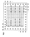
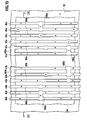
- unit cells 12A, 12B, 12C, 12D, 12E, 12F, ..., 112A, 112B, 112C, 112D, 112E, 112F, ..., 113A, 113B, 113C, 113D, 113E, 113F, ..., 114A, 114B, 114C, 114D, 114E, 114F, and so forth are respectively arranged to compose a gate array.
- I/O cells 73A, 73B, 73C, ..., 74A, 74B, 74C, ..., 83A, 83B, 83C, ..., 84A, 84B, 84C, and so forth are respectively arranged, and the I/O cells can compose input buffers, output buffers, bidirectional buffers, and the like depending on respective terminals, by use of wiring masks.
- the unit cell 12A includes a semiconductor substrate 10, a buried insulator 30 disposed on the semiconductor substrate 10, a first ridge 41a, a second ridge 42a, a third ridge 43a, a fourth ridge 44a, a fifth ridge 45a, and a sixth ridge 46a which are disposed on the buried insulator 30 and extend mutually parallel.
- Each of the first to sixth ridges 41a - 46a is made of semiconductor.
- the unit cell 12A includes insulating layers 75a, 76a, 77a, 78a, 79a, and 80a respectively disposed on the first to sixth ridges 41a to 46a, a first gate line 63a extending in a direction orthogonal to the first to sixth ridges 41a to 46a and disposed above the first to fourth ridges 41a to 44a, and a second gate line 64a extending in the direction orthogonal to the first to sixth ridges 41a to 46a and disposed above the third to sixth ridges 43a to 46a.
- the "ridge” means a fin or a plate semiconductor region.
- the first ridge 41a, the insulating layer 75a, and the first gate line 63a collectively implement a first capacitor C 1A .
- the sixth ridge 46a, the insulating layer 80a, and the second gate line 64a collectively implement a second capacitor C 2A .
- the second and third ridges 42a and 43a, the insulating layers 76a and 77a, and the first gate line 63a implement a first driver transistor Q D1A and a first load transistor Q L1A .
- the fourth and fifth ridges 44a and 45a, the insulating layers 78a and 79a, and the second gate line 64a implement a second load transistor Q L2A and a second driver transistor Q D2A .
- Isolated doped regions are provided in the second ridge 42a.
- the isolated doped regions have opposite conductivity to the conductivity of the p-type second ridge 42a.
- the isolated doped regions implement an n + source region 152a and an n + drain region 151a of the first driver transistor Q D1A , respectively. Therefore, the first driver transistor Q D1A is an n-channel MOS transistor, which includes the n + source region 152a and the n + drain region 151a self aligned by the first gate line 63a.
- Isolated doped regions are provided in the third ridge 43a.
- the isolated doped regions have opposite conductivity to the conductivity of the n-type third ridge 43a.
- the isolated doped regions implement a p + source region 201a and a p + drain region 202a of the first load transistor Q L1A , respectively. Therefore, the first load transistor Q L1A is a p-channel MOS transistor, which includes an n-type impurity region 65a provided in the third ridge 43a, the p + source region 201a and the p + drain region 202a self aligned by the first gate line 63a.
- Isolated doped regions are provided in the fifth ridge 45a.
- the isolated doped regions have opposite conductivity to the conductivity of the p-type fifth ridge 45a.
- the isolated doped regions implement an n + source region 58a and an n + drain region 57a of the second driver transistor Q D2A , respectively. Therefore, the second driver transistor Q D2A is an n-channel MOS transistor, which includes the n + source region 58a and the n + drain region 57a self aligned by the second gate line 64a.
- Isolated doped regions are provided in the fourth ridge 44a.
- the isolated doped regions have opposite conductivity to the conductivity of the n-type fourth ridge 44a.
- the isolated doped regions implement a p + source region 210a and a p + drain region 203a of the second load transistor Q L2A , respectively. Therefore, the second load transistor Q L2A is a p-channel MOS transistor, which includes an n-type impurity region 66a provided in the fourth ridge 44a, the p + source region 210a and the p + drain region 203a self aligned by the second gate line 64a.
- n + drain region 151a of the first driver transistor Q D1A , the p + drain region 202a of the first load transistor Q L1A , and the second gate line 64a are electrically interconnected by a drain line 25a disposed on the second ridge 42a and on the third ridge 43a.
- n + drain region 57a of the second driver transistor Q D2A , the p + drain region 203a of the second load transistor Q L2A , and the first gate line 63a are electrically interconnected by a drain line 26a disposed on the fourth ridge 44a and on the fifth ridge 45a.
- a first transfer transistor Q T1A is provided at the second ridge 42a, adjacent to the first driver transistor Q D1A .
- the first transfer transistor Q T1A is an n-channel MOS transistor, which includes an n + source region 150a, an n + drain region 151a, and a gate electrode 81.
- the n + source region 150a and the n + drain region 151a are provided in the second ridge 42a and self aligned by the gate electrode 81.
- the gate electrode 81 is disposed on the insulating layers 76a.
- a second transfer transistor Q T2A is provided at the fifth ridge 45a, adjacent to the second driver transistor Q D2A .
- the second transfer transistor Q T2A is an n-channel MOS transistor, which includes an n + source region 56a, an n + drain region 57a, and a gate electrode 71a.
- the n + source region 56a and the n + drain region 57a are provided in the fifth ridge 45a and self aligned by the gate electrode 71a.
- the gate electrode 71a is disposed on the insulating layers 79a.
- an n + semiconductor region 59a is provided in the first ridge 41a, adjacent to the first capacitor C 1A .
- An n + semiconductor region 55a is provided in the sixth ridge 46a, adjacent to the second capacitor C 2A .
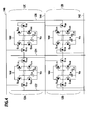
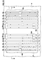
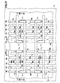
- Fig. 4 is a circuit diagram showing a part of an SRAM cell array according to the embodiment
- Fig. 5 is a plan view of the SRAM cell array corresponding to the circuit diagram shown in Fig. 4.
- a portion surrounded by a dashed rectangle corresponds to the unit cell 12A shown in Fig. 2.
- the unit cell 12A, and unit cells 12B, 12C, and 12D which are respectively equivalent to the unit cell 12A, are arranged in rows and columns and interconnected by metal wiring.
- a first interlevel insulator 101 is disposed on the buried insulator 30. Also, a second interlevel insulator 102 is disposed on the first interlevel insulator 101, a third interlevel insulator 103 is disposed on the second interlevel insulator 102. It should be noted that Fig. 5 is a perspective view obtained by seeing through the first to third interlevel insulators 101 to 103.
- the n + semiconductor region 59a adjacent to the first capacitor C 1A is electrically connected to the n + source region 152a of the first driver transistor Q D1A by a terminal area 185a interconnecting the first ridge 41a and the second ridge 42a.
- a contact stud 170a to be electrically connected to a low voltage level supply (VSS) is disposed on the terminal area 185a.
- a contact stud 283a penetrating the first interlevel insulator 101, a contact stud 281a electrically connected to the contact stud 283a and penetrating the second interlevel insulator 102, and a contact stud 171a electrically connected to the contact stud 281a and penetrating the third interlevel insulator 103 are disposed above the p + source region 201a of the first load transistor Q L1A , and the p + source region 201a is electrically connected to a high voltage level supply (VDD) through the contact studs 283a, 281a, and 171a.
- VDD high voltage level supply
- the n + semiconductor region 55a adjacent to the second capacitor C 2A is electrically connected to the n + source region 58a of the second driver transistor Q D2A by a terminal area 186a connecting the sixth ridge 46a to the fifth ridge 45a.
- a contact stud 173a to be electrically connected to the low voltage level supply (VSS) is disposed on the terminal area 186a.
- a contact stud 172a to be electrically connected to the high voltage level supply (VDD) is disposed on the p + source region 210a of the second load transistor Q L2A .
- the n + semiconductor region 55a adjacent to the second capacitor C 2A is electrically connected to the low voltage level supply (VSS), and the second driver transistor Q D2A and the second load transistor Q L2A collectively compose a CMOS inverter.
- VSS low voltage level supply
- a contact stud 302a penetrating the first interlevel insulator 101 is disposed on the n + source region 150a of the first transfer transistor Q T1A which shares the n + drain region 151a with the first driver transistor Q D1A , and a bit line 124 electrically connected to the contact stud 302a and extending in a direction perpendicular to the first to sixth ridges 41a to 46a as shown in Fig. 5 is disposed above the first interlevel insulator 101.
- the gate electrode 81 of the first transfer transistor Q T1A is electrically connected to a word line 144 through a contact stud 321.
- the gate electrode 81 and the first ridge 41a are electrically isolated owing to the insulating layer 75a disposed on the first ridge 41a.
- a contact stud 301a is disposed on the n + source region 56a of the second transfer transistor Q T2A which shares the n + drain region 57a with the second driver transistor Q D2A , and the n + source region 56a is electrically connected to a bit line 122 extending in a direction perpendicular to the first to sixth ridges 41a to 46a.
- a contact stud 261a penetrating the first interlevel insulator 101, and a contact stud 311a electrically connected to the contact stud 261a and penetrating the second interlevel insulator 102 are disposed above the gate electrode 71a of the second transfer transistor Q T2A .
- a word line 146 extending in a direction parallel to the first to sixth ridges 41a to 46a is disposed on the second interlevel insulator 102 and is electrically connected to the gate electrode 71a through the contact studs 261a and 311a.
- the CMOS inverter including the first driver transistor Q D1A and the first load transistor Q L1A , and the CMOS inverter including the second driver transistor Q D2A and the second load transistor Q L2A collectively compose a bistable flip-flop.
- the first gate line 63a, the drain line 26a, and the n + drain region 57a collectively compose one storage node of the unit cell 12A.
- the second gate line 64a, the drain line 25a, and the n + drain region 151a collectively compose the other storage node of the unit cell 12A.
- the unit cell 12B includes a first ridge 41b, a second ridge 42b, a third ridge 43b, a fourth ridge 44b, a fifth ridge 45b, and a sixth ridge 46b, which are made of a semiconductor and extending mutually parallel, insulating layers 75b, 76b, 77b, 78b, 79b, and 80b respectively disposed on the first to sixth ridges 41b to 46b, a first gate line 63b extending in a direction orthogonal to the first to sixth ridges 41b to 46b and disposed above the first to fourth ridges 41b to 44b, and a second gate line 64b extending in the direction orthogonal to the first to sixth ridges 41b to 46b and disposed above the third to sixth ridges 43b to 46b.
- the first ridge 41b, the insulating layer 75b, and the first gate line 63b collectively implement a first capacitor C 1B .
- the sixth ridge 46b, the insulating layer 80b, and the second gate line 64b collectively implement a second capacitor C 2B .
- the second and third ridges 42b and 43b, the insulating layers 76b and 77b, and the first gate line 63b implement a first driver transistor Q D1B and a first load transistor Q L1B .
- the fourth and fifth ridges 44b and 45b, the insulating layers 78b and 79b, and the second gate line 64b implement a second load transistor Q L2B and a second driver transistor Q D2B .
- the first driver transistor Q D1B is an n-channel MOS transistor, which includes an n + drain region 151b, an n + source region 152b, and the insulating layer 76b.
- the n + drain region 151b and the n + source region 152b are provided in the p-type second ridge 42b.
- the n + semiconductor region 59b is electrically connected to the n + source region 152b through a terminal area 185b.
- a contact stud 170b to be electrically connected to the low voltage level supply (VSS) is disposed on the terminal area 185b.
- the first load transistor Q L1B shown in Figs. 5 and 6 is a p-channel MOS transistor including an n-type impurity region 65b, a p + drain region 202b, a p + source region 201b, and the insulating layer 77b.
- the n-type impurity region 65b, the p + drain region 202b, and the p + source region 201b are provided in the third ridge 43b.
- a contact stud 171b to be electrically connected to the high voltage level supply (VDD) is disposed on the p + source region 201b.
- VDD high voltage level supply
- the p + drain region 202b of the first load transistor Q L1B is electrically connected to the n + drain region 151b of the first driver transistor Q D1B by a drain line 25b.
- the first driver transistor Q D1B and the first load transistor Q L1B collectively compose a CMOS inverter.
- an n + semiconductor region 55b is provided in the sixth ridge 46b, adjacent to the region where the second capacitor C 2B is provided.
- the second driver transistor Q D2B is an n-channel MOS transistor, which includes an n + drain region 57b and an n + source region 58b provided in the p-type fifth ridge 45b.
- the n + semiconductor region 55b is electrically connected to the n + source region 58b through a terminal area 186b.
- a contact stud 173b to be electrically connected to the low voltage level supply (VSS) is disposed on the terminal area 186b.
- the second load transistor Q L2B is a p-channel MOS transistor including a p + drain region 203b and a p + source region 210b, which are provided in the fourth ridge 44b.
- a contact stud 172b to be electrically connected to the high voltage level supply (VDD) is disposed on the p + source region 210b.
- the p + drain region 203b of the second load transistor Q L2B is electrically connected to the n + drain region 57b of the second driver transistor Q D2B by a drain line 26b.
- a first transfer transistor Q T1B which is an n-channel MOS transistor including an n + source region 150b, the n + drain region 151b, and the gate electrode 81, is provided at the second ridge 42b.
- a contact stud 302b is disposed on the source region 150b of the first transfer transistor Q T1B , whereby the source region 150b is electrically connected to the bit line 124.
- the first transfer transistor Q T1B shares the gate electrode 81 with the first transfer transistor Q T1A of the unit cell 12A, and is electrically connected to the word line 144.
- a second transfer transistor Q T2B which is an n-channel MOS transistor including an n + source region 56b, the n + drain region 57b, and a gate electrode 71b, is provided at the p-type fifth ridge 45b.
- a contact stud 301b is disposed on the source region 56b of the second transfer transistor Q T2B , whereby the source region 56b is electrically connected to the bit line 122.
- a contact stud 261b penetrating the first interlevel insulator 101, and a contact stud 311b electrically connected to the contact stud 261b and penetrating the second interlevel insulator 102 are disposed above the gate electrode 71b of the second transfer transistor Q T2B .
- the gate electrode 71b is electrically connected to a word line 142 through the contact studs 261b and 311b.
- n + drain region 151b of the first driver transistor Q D1B , the p + drain region 202b of the first load transistor Q L1B , and the second gate line 64b are electrically interconnected by a drain line 25b disposed above the second ridge 42b and above the third ridge 43b.
- n + drain region 57b of the second driver transistor Q D2B , the p + drain region 203b of the second load transistor Q L2B , and the first gate line 63b are electrically interconnected by a drain line 26b disposed above the fourth ridge 44b and above the fifth ridge 45b.
- the CMOS inverter including the first driver transistor Q D1B and the first load transistor Q L1B , and the CMOS inverter including the second driver transistor Q D2B and the second load transistor Q L2B collectively compose a bistable flip-flop.
- the first gate line 63b, the drain line 26b, and the n + drain region 57b collectively compose one storage node of the unit cell 12B.
- the second gate line 64b, the drain line 25b, and the n + drain region 151b collectively compose the other storage node of the unit cell 12B.
- the unit cell 12C shown in Figs. 5, 8, 9 and 10 includes the first ridge 41a, the second ridge 42a, the third ridge 43a, the fourth ridge 44a, the fifth ridge 45a, the sixth ridge 46a, a first capacitor C 1C provided at the first ridge 41a, a first transfer transistor Q T1C and a first driver transistor Q D1C provided at the second ridge 42a, a first load transistor Q L1C provided at the third ridge 43a, a second load transistor Q L2C provided at the fourth ridge 44a, a second transfer transistor Q T2C and a second driver transistor Q D2C provided at the fifth ridge 45a, and a second capacitor C 2C provided at the sixth ridge 46a.
- the first capacitor C 1C provided at the first ridge 41a as shown in Figs. 5 and 8 includes the insulating layer 75a and a first gate line 63c. Meanwhile, an n + semiconductor region 59c is disposed in the first ridge 41a, adjacent to the region where the first capacitor C 1C is provided.
- the first driver transistor Q D1C provided at the second ridge 42a as shown in Figs. 5 and 9 is an n-channel MOS transistor, which includes an n + drain region 151c, an n + source region 152c, the insulating layer 76a, and the first gate line 63c.
- the n + source region 152c is electrically connected to the n + semiconductor region 59c through a terminal area 185c.
- a contact stud 170c to be electrically connected to the low voltage level supply (VSS) is disposed on the terminal area 185c.
- the first load transistor Q L1C provided at the third ridge 43a as shown in Figs. 5 and 10 is a p-channel MOS transistor including the n-type impurity region 65a, a p + drain region 202c, a p + source region 201c, the insulating layer 77a, and the first gate line 63c.
- the contact stud 283a penetrating the first interlevel insulator 101, the contact stud 281a electrically connected to the contact stud 283a and penetrating the second interlevel insulator 102, and a contact stud 171c electrically connected to the contact stud 281a and penetrating the third interlevel insulator 103 are disposed above the p + source region 201c, and the p + source region 201c is electrically connected to the high voltage level supply (VDD).
- the p + drain region 202c of the first load transistor Q L1C is electrically connected to the n + drain region 151c of the first driver transistor Q D1C by a drain line 25c.
- the first transfer transistor Q T1C provided at the second ridge 42a as shown in Figs. 5 and 9 is an n-channel MOS transistor, which includes the n + source region 150a, the n + drain region 151c, the insulating layer 76a, and a gate electrode 82.
- a contact stud 322 is disposed on the gate electrode 82, and the gate electrode 82 is electrically connected to the word line 144.
- the second capacitor C 2C provided at the sixth ridge 46a as shown in Fig. 5 includes a second gate line 64c.
- the n + semiconductor region 55a is provided in the sixth ridge 46a, adjacent to the region where the second capacitor C 2C is provided.
- the second driver transistor Q D2C provided at the fifth ridge 45a is an n-channel MOS transistor, which includes an n + drain region 57c, the n + source region 58a, and the second gate line 64c.
- the second load transistor Q L2C provided at the fourth ridge 44a is a p-channel MOS transistor, which includes a p + drain region 203c, a p + source region 210c, and the second gate line 64c.
- the p + drain region 203c of the second load transistor Q L2C is electrically connected to the n + drain region 57c of the second driver transistor Q D2C by a drain line 26c.
- the second transfer transistor Q T2C provided at the fifth ridge 45a is an n-channel MOS transistor, which includes an n + source region 56c, the n + drain region 57c, and a gate electrode 71c.
- a contact stud 301c is disposed on the n + source region 56c, whereby the n + source region 56c is electrically connected to a bit line 126.
- a contact stud 311c is disposed on the gate electrode 71c, whereby the gate electrode 71c is electrically connected to the word line 146
- the unit cell 12D shown in Fig. 5 includes the first ridge 41b, the second ridge 42b, the third ridge 43b, the fourth ridge 44b, the fifth ridge 45b, the sixth ridge 46b, a first capacitor C 1D provided at the first ridge 41b, a first transfer transistor Q T1D and a first driver transistor Q D1D provided at the second ridge 42b, a first load transistor Q L1D provided at the third ridge 43b, a second load transistor Q L2D provided at the fourth ridge 44b, a second transfer transistor Q T2D and a second driver transistor Q D2D provided at the fifth ridge 45b, and a second capacitor C 2D provided at the sixth ridge 46b.
- the first capacitor C 1D provided at the first ridge 41b includes a first gate line 63d. Meanwhile, an n + semiconductor region 59d is provided in the first ridge 41b, adjacent to the region where the first capacitor C 1D is provided.
- the first driver transistor Q D1D provided at the second ridge 42b is an n-channel MOS transistor, which includes an n + drain region 151d, an n + source region 152d, and the first gate line 63d.
- the n + semiconductor region 59d is electrically connected to the n + source region 152d through a terminal area 185d.
- the first load transistor Q L1D provided at the third ridge 43b is a p-channel MOS transistor including a p + drain region 202d, a p + source region 201d, and the first gate line 63d.
- the p + drain region 202d of the first load transistor Q L1D is electrically connected to the n + drain region 151d of the first driver transistor Q D1D by a drain line 25d.
- the first transfer transistor Q T1D provided at the second ridge 42b is an n-channel MOS transistor, which includes the n + source region 150b, the n + drain region 151d, and the gate electrode 82.
- the second capacitor C 2D provided at the sixth ridge 46b includes a second gate line 64d.
- the n + semiconductor region 55b is provided in the sixth ridge 46b, adjacent to the region where the second capacitor C 2D is disposed.
- the second driver transistor Q D2D provided at the fifth ridge 45b is an n-channel MOS transistor, which includes an n + drain region 57d, the n + source region 58b, and the second gate line 64d.
- the second load transistor Q L2D provided at the fourth ridge 44b is a p-channel MOS transistor, which includes a p + drain region 203d, a p + source region 210d, and the second gate line 64d.
- the p + drain region 203d of the second load transistor Q L2D is electrically connected to the n + drain region 57d of the second driver transistor Q D2D by a drain line 26d.
- the second transfer transistor Q T2C is an n-channel MOS transistor, which includes the fifth ridge 45b, an n + source region 56d, the n + drain region 57d, and a gate electrode 71d.
- a contact stud 301d is disposed on the source region 56d, whereby the n + source region 56d is electrically connected to the bit line 126.
- a contact stud 311d is disposed on the gate electrode 71d, whereby the gate electrode 71d is electrically connected to the word line 142.
- the semiconductor memory shown in Figs. 5 to 10 it is possible to use single-crystal silicon (Si) or the like as the material for the semiconductor substrate 10.
- Si single-crystal silicon
- a single layer made of polycrystalline silicone or a double layer formed by depositing a silicide layer on a polycrystalline silicon layer can be used for the first gate lines 63a, 63b, 63c, and 63d, the second gate lines 64a, 64b, 64c, and 64d, and the gate electrodes 71a, 71b, 71c, 71d, 81 and 82 respectively.
- the material for each of the first interlevel insulator 101, the second interlevel insulator 102, and the third interlevel insulator 103 it is possible to use an inorganic insulating material such as silicon dioxide (SiO 2 ), carbon-incorporated silicon oxide (SiOC), fluorine-incorporated silicon oxide (SiOF), a so-called low dielectric (low-k) material such as silicon dioxide hydrogen silsesquioxane (HSQ) and other organic polymers, or the like.
- silicon dioxide SiO 2
- SiOC carbon-incorporated silicon oxide
- SiOF fluorine-incorporated silicon oxide
- low-k low dielectric
- the one storage node in the unit cell 12A having the n + drain region 57a of the second driver transistor Q D2A includes the first capacitor C 1A .
- the first capacitor C 1A is electrically connected to the low voltage level supply (VSS) through the n + semiconductor region 59a. Therefore, even if electrons are generated in the n + drain region 57a due to the impingement of alpha particles or the like into the semiconductor memory, it is possible to effectively absorb the generated electrons by the first capacitor C 1A . Consequently, it is possible to effectively prevent soft errors.
- a similar effectiveness is achieved in the other storage node having the n + drain region 151a of the first driver transistor Q D1A , owing to the second capacitor C 2A .
- it is possible to prevent soft errors owing to the first capacitors C 1B , C 1C , and C 1D , and the second capacitors C 2B , C 2C , and C 2D .
- first ridges 41a and 41b, and the sixth ridges 46a and 46b, where the first capacitors C 1A , C 1B , C 1C , and C 1D , and the second capacitors C 1B , C 2B , C 2C , and C 2D are provided have been provided for the purpose of dealing with lithographic errors in the manufacturing process of semiconductor memory. Therefore, according to the semiconductor memory of the embodiment, it is possible to suppress soft errors by the first capacitors C 1A , C 1B , C 1C , and C 1D , and the second capacitors C 1B , C 2B , C 2C , and C 2D without causing an increase in the cell area as compared to earlier semiconductor memories.
- the respective unit cells 12A to 12C include six ridges of the first to sixth ridges 41a to 46a or 41b to 46b.
- the embodiment of the present invention is not limited to the unit cells including six ridges. In respect of effective utilization of ridges on both ends inside a unit cell disposed for the purpose of dealing with lithographic errors, the present invention is also applicable to a unit cell including six or more ridges.
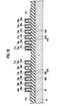
- the buried insulator 30 and a p-type semiconductor layer 20 on the buried insulator 30 are formed using thermal oxidization or furnace processing for example after oxygen ions are doped into the p-type semiconductor substrate 10.
- the semiconductor layer 20 is composed of Si, for example.
- a photoresist is applied to the surface of the p-type semiconductor layer 20 to define a pattern through use of optical lithography to produce chemical etchant masks 91a, 91b, 91c, 91d, 93a, 93b, 93c, 93d.
- chemical etchant masks 91a - 93d are defined, an etch process is employed to selectively remove the semiconductor layer 20 with the etching stop on the buried insulator 30.
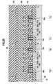
- Fig. 13 and Fig. 14 which is a sectional view taken on line XIV-XIV in Fig. 13, the first ridges 41a and 41b, the second ridges 42a and 42b, the third ridges 43a and 43b, the fifth ridges 45a and 45b, the fourth ridges 44a and 44b, the sixth ridges 46a and 46b, and the terminal areas 185a - 185d, 186a and 186b are formed.
- a first mask resist capping the first ridges 41a and 41b, the second ridges 42a and 42b, the sixth ridges 46a and 46b, and the fifth ridges 45a and 45b is formed through use of optical lithography. Thereafter, the third ridges 43a and 43b and the fourth ridges 44a and 44b are selectively doped with N-type dopants as first dopants. Phosphorus ions (P + ) and Arsenic ions (As + ) can be used for the first dopants, for example.
- the doped first dopants are annealed and first silicon oxide layers overlying the first to sixth ridges 41a - 46a and 41b - 46b, and the terminal areas 185a - 185d, 186a, and 186b are formed.
- the first silicon oxide layers are removed, as shown in Fig. 15 and Fig. 16 which is a sectional view taken on line XVI-XVI in Fig. 15, the n-type impurity regions 65a, 65b, 66a, 66b are formed in the third ridges 43a, 43b, and the fourth ridges 44a, 44b.
- the insulating layers 75a - 80b overlying the first ridges 41a, 41b, the second ridges 42a, 42b, the third ridges 43a, 43b, the fifth ridges 45a, 45b, the fourth ridges 44a, 44b, the sixth ridges 46a, 46b, and the terminal areas 185a - 185d, 186a, 186b are grown by the thermal oxidation.
- a first polycrystalline silicon layer is deposited on the buried insulator 30 by Chemical Vapor Deposition (CVD) process. Thereafter, the first polycrystalline silicon layer is selectively removed by use of the optical lithography and the anisotropic etch process. Accordingly, as shown in Fig. 17, Fig.
- Fig. 17 is a perspective view through the insulating layers 75a - 80a, 75b - 80b.
- a second mask resist is formed and the first ridges 41a, 41b, the second ridges 42a, 42b, the fifth ridges 45a, 45b, and the portion of the sixth ridges 46a, 46b are doped with the first dopants using the first gate lines 63a - 63d, the second gate lines 64a - 64d, and the gate electrodes 71a - 71d, 81, 82 as a doping mask.
- the second mask resist is removed by the ash process.
- a third mask resist is formed and the third ridges 43a, 43b and the fourth ridges 44a, 44b are selectively doped with P-type dopants as second dopants using the first gate lines 63a - 63d, the second gate lines 64a - 64d, and the gate electrodes 71a - 71d, 81, 82 as the doping mask.
- Boron ions (B + ) can be used for the second dopants.
- the insulating layers 75a - 80a, 75b -80b are selectively removed and the third mask resist is removed by the ash process.
- Fig. 20 which is a sectional view taken on line XXII-XXII in Fig. 20
- Fig. 22 which is a sectional view taken on line XXIII- XXIII in Fig. 20
- Fig. 23 which is a sectional view taken on line XXIV- XXIV in Fig. 20
- Fig. 24 which is a sectional view taken on line XXV- XXV in Fig. 20
- the annealing process is employed to activate the doped first and second dopants and diffuse the doped first and second dopants in the first to sixth ridges 41a - 46a, 41b - 46b.
- the n + semiconductor region 55a, 55b, 59a - 59d is formed in the first riges 41a, 41b and the second ridges 46a, 46b.
- the n + source region 56a - 56d, 58a, 58b, 150a, 150b, 152a - 152d, the n + drain region 57a - 57d, 151a - 151d, the p + source region 201a - 201d, 210a, 210b, and the p + drain region 202a - 202d, 203a - 203d are formed in the second to fifth ridges 42a - 45a, 42b - 45b and self aligned by the first gate lines 63a - 63d, the second gate lines 64a - 64d, the gate electrodes 71a - 71d, 81, 82.
- the first transfer transistor Q T1A - Q T1D , the second transfer transistor Q T2A - Q T2D , the first driver transistor Q D1A - Q D1C , the second driver transistor Q D2A - Q D2D , the first load transistor Q L1A - Q L1D , the second load transistor Q L2A - Q L2D are provided.
- the sectional view taken on line XXI-XXI in Fig. 20 is same as Fig. 18.
- a second silicon oxide layer capping the first ridges 41a, 41b, the second ridges 42a, 42b, the third ridges 43a, 43b, the fifth ridges 45a, 45b, the fourth ridges 44a, 44b, and the terminal areas 185a - 185d, 186a, 186b and grown by the annealing process is removed. Thereafter, a fourth mask resist is formed.
- a second polycrystalline silicon layer is selectively deposited on the buried insulator 30 by using the fourth mask resist.
- the fourth mask resist is removed by the ash process, as shown in Fig. 25 and Fig. 26 which is a sectional view taken on line XXVI-XXVI in Fig. 25, the drain line 25a - 25d, 26a - 26d are formed.
- the sectional view taken on line XVIII-XVIII in Fig. 25 is same as Fig. 18.
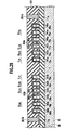
- the first interlevel insulator 101 is deposited on the buried insulator 30 by the CVD process. Then, chemical mechanical planarization (CMP) process is employed to produce the planar surface of the first interlevel insulator 101. Thereafter, via holes are delineated in the first interlevel insulator 101 by use of the optical lithography and the anisotropic etch process. The via holes are filled with the refractory metal such as Mo and W by the sputtering or vaporization process. The excess refractory metal remaining on the first interlevel insulator 101 is removed by the CMP process.
- CMP chemical mechanical planarization
- the contact studs 169a - 169d, 172a, 172b, 173a, 173b, 261a - 261d, 283a - 283d, 301a - 301d, 302a, 302b, 361, 362 are formed in the first interlevel insulator 101.
- the electric conductor such as Al, Al-Si, and Al-Cu-Si is deposited on the first interlevel insulator 101 by the sputtering or vaporization process.
- the deposited electric conductor is selectively removed by use of the optical lithography and the anisotropic etch process to form the bit lines 122, 124, and 126, as shown in Fig. 27, Fig.
- Fig. 28 which is a sectional view taken on line XXVIII-XXVIII in Fig. 27, Fig. 29 which is a sectional view taken on line XXIX-XXIX in Fig. 27, Fig. 30 which is a sectional view taken on line XXX-XXX in Fig. 27, Fig. 31 which is a sectional view taken on line XXXI-XXXI in Fig. 27, and Fig. 32 which is a sectional view taken on line XXXII-XXXII in Fig. 27.
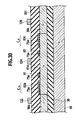
- the second interlevel insulator 102 overlying the bit lines 122, 124, 126 is deposited on the first interlevel insulator 101 by the CVD process and the CMP process is employed to produce the planar surface of the second interlevel insulator 102. Then, via holes are delineated in the second interlevel insulator 102 by use of the optical lithography and the anisotropic etch process. The via holes are filled with the refractory metal by the sputtering or vaporization process. The excess refractory metal remaining on the second interlevel insulator 102 is removed by the CMP process.
- the contact studs 170a - 170d, 283a - 283d, 311a - 311d, 321, 322 are formed in the second interlevel insulator 102.
- the electric conductor is deposited on the second interlevel insulator 102 by the sputtering or vaporization process.
- the deposited electric conductor is selectively removed by use of the optical lithography and the anisotropic etch process to form the word lines 142, 144, and 146.
- the third interlevel insulator 103 overlying the word lines 142, 144, and 146 is deposited on the second interlevel insulator 102 by the CVD process and the CMP process is employed to produce the planar surface of the third interlevel insulator 103 and consequently the semiconductor memory according to the embodiment and shown in Fig. 5 is obtained.
- the metal wiring such as bit lines 122, 124, and 126 shown in Fig. 27 are formed by the sputtering or vaporization process and the anisotropic etch process.
- the damascene process is also alternative. Specifically, delineating trenches corresponding to the pattern of the metal wiring in the interlevel insulator 101 by the lithography process, depositing copper (Cu) layer by the electroplating, and polishing the deposited Cu layer are also alternative.
- the method according to the embodiment makes it possible to form the first capacitor C 1A - C 1D and the second capacitor C 2A - C 2D at the same time when the first and second gate lines 63a - 63d and 64a - 64d are formed. Also, masks for specifically manufacturing the first capacitor C 1A - C 1D and the second capacitor C 2A - C 2D are not required. Therefore, the method according to the embodiment makes it possible to manufacture the semiconductor memory containing capacitors without increasing complexity in the manufacturing process and additional masks required in the lithography process.
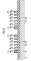
- the unit cells 12A - 12D shown in Figs. 5 to 10 are provided on the buried insulator 30.
- Fig. 33 which is a sectional view taken on line XXXIV-XXXIV in Fig. 33
- Fig. 35 which is a sectional view taken on line XXXV-XXXV in Fig. 33
- the shallow trench isolation 70 is composed of SiO 2 , for example.
- the first ridges 41a, 41b and the sixth ridges 46a, 46b are disposed on the shallow trench isolation 70.
- the second ridges 42a, 42b, the third ridges 43a, 43b, the fourth ridges 44a, 44b, and the fifth ridges 45a, 45b are disposed on the semiconductor substrate 50.
- Arrangement of other elements in the semiconductor memory is similar to the arrangement of the semiconductor memory shown in Figs. 5 to 10.
- a method for manufacturing the semiconductor memory shown in Figs. 33 to 35 is as follows.
- the shallow trench isolation 70 is formed in the semiconductor substrate 50.
- a silicon layer is deposited on the semiconductor substrate 50 and the deposited silicon layer is crystallized by the annealing process.
- the first ridges 41a, 41b, the sixth ridges 46a, 46b, the second ridges 42a, 42b, the third ridges 43a, 43b, the fifth ridges 45a, 45b, and the fourth ridges 44a, 44b are formed by the method as described with Figs. 11 and 12.
- Following processes are similar to Figs. 13 to 32.
- the semiconductor memory shown in Figs. 33 to 35 prevents delayed soft error through the semiconductor substrate 50 since the first ridges 41a, 41b and the sixth ridges 46a, 46b are disposed on the shallow trench isolation 70.
- the second ridges 42a, 42b, the third ridges 43a, 43b, the fifth ridges 45a, 45b, and the fourth ridges 44a, 44b are arranged between the first ridges 41a, 41b and the sixth ridges 46a, 46b.
- arranging the ridges provided with the capacitors between the ridges provided with the driver transistors or the load transistors is also alternative.
Landscapes
- Engineering & Computer Science (AREA)
- Power Engineering (AREA)
- Physics & Mathematics (AREA)
- Condensed Matter Physics & Semiconductors (AREA)
- General Physics & Mathematics (AREA)
- Computer Hardware Design (AREA)
- Microelectronics & Electronic Packaging (AREA)
- Manufacturing & Machinery (AREA)
- Semiconductor Memories (AREA)
- Static Random-Access Memory (AREA)
- Thin Film Transistor (AREA)
Applications Claiming Priority (2)
| Application Number | Priority Date | Filing Date | Title |
|---|---|---|---|
| JP2004115405 | 2004-04-09 | ||
| JP2004115405A JP4195409B2 (ja) | 2004-04-09 | 2004-04-09 | 半導体記憶装置 |
Publications (2)
| Publication Number | Publication Date |
|---|---|
| EP1585177A2 true EP1585177A2 (de) | 2005-10-12 |
| EP1585177A3 EP1585177A3 (de) | 2008-11-26 |
Family
ID=34909539
Family Applications (1)
| Application Number | Title | Priority Date | Filing Date |
|---|---|---|---|
| EP05252216A Withdrawn EP1585177A3 (de) | 2004-04-09 | 2005-04-08 | Halbleitervorrichtung vom "MASTERSLICE"-Typ und ein Speicherelement und Herstellungsverfahren |
Country Status (5)
| Country | Link |
|---|---|
| US (1) | US7199428B2 (de) |
| EP (1) | EP1585177A3 (de) |
| JP (1) | JP4195409B2 (de) |
| KR (1) | KR100769785B1 (de) |
| CN (1) | CN100438043C (de) |
Cited By (1)
| Publication number | Priority date | Publication date | Assignee | Title |
|---|---|---|---|---|
| EP1939942A3 (de) * | 2006-12-27 | 2010-06-23 | Samsung Electronics Co., Ltd. | Halbleiterbauelement und Herstellungsverfahren dafür |
Families Citing this family (3)
| Publication number | Priority date | Publication date | Assignee | Title |
|---|---|---|---|---|
| US7655989B2 (en) * | 2006-11-30 | 2010-02-02 | International Business Machines Corporation | Triple gate and double gate finFETs with different vertical dimension fins |
| JP5159289B2 (ja) | 2007-12-20 | 2013-03-06 | 株式会社東芝 | 不揮発性半導体記憶装置 |
| US8258572B2 (en) * | 2009-12-07 | 2012-09-04 | Taiwan Semiconductor Manufacturing Company, Ltd. | SRAM structure with FinFETs having multiple fins |
Citations (3)
| Publication number | Priority date | Publication date | Assignee | Title |
|---|---|---|---|---|
| US5677866A (en) * | 1993-12-22 | 1997-10-14 | Nec Corporation | Semiconductor memory device |
| US20030142538A1 (en) * | 2002-01-29 | 2003-07-31 | Mitsubishi Denki Kabushiki Kaisha | Semiconductor memory |
| US20030197194A1 (en) * | 2002-04-12 | 2003-10-23 | International Business Machines Corporation | Fin memory cell and method of fabrication |
Family Cites Families (3)
| Publication number | Priority date | Publication date | Assignee | Title |
|---|---|---|---|---|
| JP3472590B2 (ja) | 1993-04-05 | 2003-12-02 | Necエレクトロニクス株式会社 | 半導体記憶装置 |
| US5700707A (en) * | 1996-06-13 | 1997-12-23 | Chartered Semiconductor Manufacturing Pte Ltd. | Method of manufacturing SRAM cell structure having a tunnel oxide capacitor |
| JP4753534B2 (ja) * | 2003-12-26 | 2011-08-24 | ルネサスエレクトロニクス株式会社 | 半導体記憶装置 |
-
2004
- 2004-04-09 JP JP2004115405A patent/JP4195409B2/ja not_active Expired - Fee Related
-
2005
- 2005-04-05 US US11/098,671 patent/US7199428B2/en not_active Expired - Fee Related
- 2005-04-08 KR KR1020050029487A patent/KR100769785B1/ko not_active IP Right Cessation
- 2005-04-08 EP EP05252216A patent/EP1585177A3/de not_active Withdrawn
- 2005-04-11 CN CNB2005100641317A patent/CN100438043C/zh not_active Expired - Fee Related
Patent Citations (3)
| Publication number | Priority date | Publication date | Assignee | Title |
|---|---|---|---|---|
| US5677866A (en) * | 1993-12-22 | 1997-10-14 | Nec Corporation | Semiconductor memory device |
| US20030142538A1 (en) * | 2002-01-29 | 2003-07-31 | Mitsubishi Denki Kabushiki Kaisha | Semiconductor memory |
| US20030197194A1 (en) * | 2002-04-12 | 2003-10-23 | International Business Machines Corporation | Fin memory cell and method of fabrication |
Non-Patent Citations (3)
| Title |
|---|
| ANANTHAN H ET AL: "FinFET SRAM-device and circuit design considerations" QUALITY ELECTRONIC DESIGN, 2004. PROCEEDINGS. 5TH INTERNATIONAL SYMPOS IUM ON SAN JOSE, CALIFORNIA 22-24 MARCH 2004, PISCATAWAY, NJ, USA,IEEE, 22 March 2004 (2004-03-22), pages 511-516, XP010695543 ISBN: 978-0-7695-2093-3 * |
| LUDWIG T ET AL: "Finfet technology for future microprocessors" 2003 IEEE INTERNATIONAL SOI CONFERENCE PROCEEDINGS. NEWPORT BEACH, CA, SEPT. 29 - OCT. 2, 2003; [IEEE INTERNATIONAL SOI CONFERENCE], NEW YORK, NY : IEEE, US, 29 September 2003 (2003-09-29), pages 33-34, XP010665921 ISBN: 978-0-7803-7815-5 * |
| NOWAK E J ET AL: "Turning silicon on its edge" IEEE CIRCUITS AND DEVICES MAGAZINE, IEEE SERVICE CENTER, PISCATAWAY, NJ, US, vol. 20, no. 1, 1 January 2004 (2004-01-01), pages 20-31, XP011106768 ISSN: 8755-3996 * |
Cited By (2)
| Publication number | Priority date | Publication date | Assignee | Title |
|---|---|---|---|---|
| EP1939942A3 (de) * | 2006-12-27 | 2010-06-23 | Samsung Electronics Co., Ltd. | Halbleiterbauelement und Herstellungsverfahren dafür |
| US7829932B2 (en) | 2006-12-27 | 2010-11-09 | Samsung Electronics Co., Ltd. | Semiconductor device |
Also Published As
| Publication number | Publication date |
|---|---|
| CN1681127A (zh) | 2005-10-12 |
| US20050226075A1 (en) | 2005-10-13 |
| KR100769785B1 (ko) | 2007-10-24 |
| EP1585177A3 (de) | 2008-11-26 |
| CN100438043C (zh) | 2008-11-26 |
| JP2005302934A (ja) | 2005-10-27 |
| KR20060046656A (ko) | 2006-05-17 |
| JP4195409B2 (ja) | 2008-12-10 |
| US7199428B2 (en) | 2007-04-03 |
Similar Documents
| Publication | Publication Date | Title |
|---|---|---|
| US6515511B2 (en) | Semiconductor integrated circuit and semiconductor integrated circuit device | |
| KR100357336B1 (ko) | 반도체 집적회로장치 | |
| US6063686A (en) | Method of manufacturing an improved SOI (silicon-on-insulator) semiconductor integrated circuit device | |
| JP5086625B2 (ja) | 半導体装置の製造方法 | |
| US20050124095A1 (en) | Sram device having high aspect ratio cell boundary | |
| JPS62274773A (ja) | 半導体記憶装置 | |
| JP5847550B2 (ja) | 半導体装置および半導体装置の製造方法 | |
| JP2013105981A (ja) | 半導体装置 | |
| JP4237595B2 (ja) | スタティックランダムアクセスメモリ | |
| EP1585177A2 (de) | Halbleitervorrichtung vom "MASTERSLICE"-Typ und ein Speicherelement und Herstellungsverfahren | |
| CN112786605B (zh) | 局部字线驱动器件、存储器件及其制造方法 | |
| CN114497040A (zh) | 半导体器件 | |
| US7250661B2 (en) | Semiconductor memory device with plural source/drain regions | |
| JP2018152450A (ja) | 半導体装置の製造方法 | |
| US20230081960A1 (en) | Vertical channel transistor | |
| US20240136287A1 (en) | Local VDD And VSS Power Supply Through Dummy Gates with Gate Tie-Downs and Associated Benefits | |
| JP2749087B2 (ja) | 半導体集積回路装置 | |
| JP3839418B2 (ja) | 半導体集積回路装置の製造方法 | |
| JP2016021590A (ja) | 半導体記憶装置 | |
| CN116266994A (zh) | 高性能运算和高储存容量的同构/异构集成电路系统 | |
| KR20240022735A (ko) | 반도체 장치 | |
| JP2004146844A (ja) | 半導体集積回路装置の製造方法 | |
| JPH04306863A (ja) | 半導体集積回路装置 | |
| JP2007258739A (ja) | 半導体集積回路装置 |
Legal Events
| Date | Code | Title | Description |
|---|---|---|---|
| PUAI | Public reference made under article 153(3) epc to a published international application that has entered the european phase |
Free format text: ORIGINAL CODE: 0009012 |
|
| AK | Designated contracting states |
Kind code of ref document: A2 Designated state(s): AT BE BG CH CY CZ DE DK EE ES FI FR GB GR HU IE IS IT LI LT LU MC NL PL PT RO SE SI SK TR |
|
| AX | Request for extension of the european patent |
Extension state: AL BA HR LV MK YU |
|
| PUAL | Search report despatched |
Free format text: ORIGINAL CODE: 0009013 |
|
| AK | Designated contracting states |
Kind code of ref document: A3 Designated state(s): AT BE BG CH CY CZ DE DK EE ES FI FR GB GR HU IE IS IT LI LT LU MC NL PL PT RO SE SI SK TR |
|
| AX | Request for extension of the european patent |
Extension state: AL BA HR LV MK YU |
|
| RIC1 | Information provided on ipc code assigned before grant |
Ipc: H01L 27/118 20060101ALI20081023BHEP Ipc: H01L 27/12 20060101ALI20081023BHEP Ipc: H01L 21/84 20060101ALI20081023BHEP Ipc: H01L 27/11 20060101AFI20081023BHEP |
|
| 17P | Request for examination filed |
Effective date: 20090402 |
|
| 17Q | First examination report despatched |
Effective date: 20090609 |
|
| AKX | Designation fees paid |
Designated state(s): DE FR GB |
|
| STAA | Information on the status of an ep patent application or granted ep patent |
Free format text: STATUS: THE APPLICATION IS DEEMED TO BE WITHDRAWN |
|
| 18D | Application deemed to be withdrawn |
Effective date: 20091020 |