EP1584929A2 - Phasendetektor mit Digitaloszillator - Google Patents
Phasendetektor mit Digitaloszillator Download PDFInfo
- Publication number
- EP1584929A2 EP1584929A2 EP05002023A EP05002023A EP1584929A2 EP 1584929 A2 EP1584929 A2 EP 1584929A2 EP 05002023 A EP05002023 A EP 05002023A EP 05002023 A EP05002023 A EP 05002023A EP 1584929 A2 EP1584929 A2 EP 1584929A2
- Authority
- EP
- European Patent Office
- Prior art keywords
- signal
- phase
- digital
- frequency
- output
- Prior art date
- Legal status (The legal status is an assumption and is not a legal conclusion. Google has not performed a legal analysis and makes no representation as to the accuracy of the status listed.)
- Withdrawn
Links
Images


Classifications
-
- H—ELECTRICITY
- H03—ELECTRONIC CIRCUITRY
- H03L—AUTOMATIC CONTROL, STARTING, SYNCHRONISATION OR STABILISATION OF GENERATORS OF ELECTRONIC OSCILLATIONS OR PULSES
- H03L7/00—Automatic control of frequency or phase; Synchronisation
- H03L7/06—Automatic control of frequency or phase; Synchronisation using a reference signal applied to a frequency- or phase-locked loop
- H03L7/08—Details of the phase-locked loop
- H03L7/085—Details of the phase-locked loop concerning mainly the frequency- or phase-detection arrangement including the filtering or amplification of its output signal
-
- G—PHYSICS
- G01—MEASURING; TESTING
- G01R—MEASURING ELECTRIC VARIABLES; MEASURING MAGNETIC VARIABLES
- G01R25/00—Arrangements for measuring phase angle between a voltage and a current or between voltages or currents
- G01R25/04—Arrangements for measuring phase angle between a voltage and a current or between voltages or currents involving adjustment of a phase shifter to produce a predetermined phase difference, e.g. zero difference
-
- G—PHYSICS
- G01—MEASURING; TESTING
- G01R—MEASURING ELECTRIC VARIABLES; MEASURING MAGNETIC VARIABLES
- G01R31/00—Arrangements for testing electric properties; Arrangements for locating electric faults; Arrangements for electrical testing characterised by what is being tested not provided for elsewhere
- G01R31/28—Testing of electronic circuits, e.g. by signal tracer
- G01R31/317—Testing of digital circuits
- G01R31/31708—Analysis of signal quality
- G01R31/31709—Jitter measurements; Jitter generators
-
- G—PHYSICS
- G01—MEASURING; TESTING
- G01R—MEASURING ELECTRIC VARIABLES; MEASURING MAGNETIC VARIABLES
- G01R31/00—Arrangements for testing electric properties; Arrangements for locating electric faults; Arrangements for electrical testing characterised by what is being tested not provided for elsewhere
- G01R31/28—Testing of electronic circuits, e.g. by signal tracer
- G01R31/317—Testing of digital circuits
- G01R31/3181—Functional testing
- G01R31/319—Tester hardware, i.e. output processing circuits
- G01R31/31917—Stimuli generation or application of test patterns to the device under test [DUT]
- G01R31/31922—Timing generation or clock distribution
-
- H—ELECTRICITY
- H03—ELECTRONIC CIRCUITRY
- H03D—DEMODULATION OR TRANSFERENCE OF MODULATION FROM ONE CARRIER TO ANOTHER
- H03D13/00—Circuits for comparing the phase or frequency of two mutually-independent oscillations
- H03D13/003—Circuits for comparing the phase or frequency of two mutually-independent oscillations in which both oscillations are converted by logic means into pulses which are applied to filtering or integrating means
-
- H—ELECTRICITY
- H03—ELECTRONIC CIRCUITRY
- H03L—AUTOMATIC CONTROL, STARTING, SYNCHRONISATION OR STABILISATION OF GENERATORS OF ELECTRONIC OSCILLATIONS OR PULSES
- H03L7/00—Automatic control of frequency or phase; Synchronisation
- H03L7/06—Automatic control of frequency or phase; Synchronisation using a reference signal applied to a frequency- or phase-locked loop
- H03L7/08—Details of the phase-locked loop
- H03L7/085—Details of the phase-locked loop concerning mainly the frequency- or phase-detection arrangement including the filtering or amplification of its output signal
- H03L7/091—Details of the phase-locked loop concerning mainly the frequency- or phase-detection arrangement including the filtering or amplification of its output signal the phase or frequency detector using a sampling device
-
- H—ELECTRICITY
- H03—ELECTRONIC CIRCUITRY
- H03L—AUTOMATIC CONTROL, STARTING, SYNCHRONISATION OR STABILISATION OF GENERATORS OF ELECTRONIC OSCILLATIONS OR PULSES
- H03L7/00—Automatic control of frequency or phase; Synchronisation
- H03L7/06—Automatic control of frequency or phase; Synchronisation using a reference signal applied to a frequency- or phase-locked loop
- H03L7/16—Indirect frequency synthesis, i.e. generating a desired one of a number of predetermined frequencies using a frequency- or phase-locked loop
-
- H—ELECTRICITY
- H03—ELECTRONIC CIRCUITRY
- H03L—AUTOMATIC CONTROL, STARTING, SYNCHRONISATION OR STABILISATION OF GENERATORS OF ELECTRONIC OSCILLATIONS OR PULSES
- H03L7/00—Automatic control of frequency or phase; Synchronisation
- H03L7/06—Automatic control of frequency or phase; Synchronisation using a reference signal applied to a frequency- or phase-locked loop
- H03L7/08—Details of the phase-locked loop
- H03L7/085—Details of the phase-locked loop concerning mainly the frequency- or phase-detection arrangement including the filtering or amplification of its output signal
- H03L7/087—Details of the phase-locked loop concerning mainly the frequency- or phase-detection arrangement including the filtering or amplification of its output signal using at least two phase detectors or a frequency and phase detector in the loop
Definitions
- This invention relates generally to signal generation and more specifically to the synthesis of periodic signals with high signal integrity.
- ATE Automatic test equipment
- other high performance electronic systems rely upon the ability to generate precise periodic signals. ATE requires these signals for testing state-of-the-art electronic devices, such as computer chips, telecommunications chips, and electronic assemblies. As these devices and assemblies become more advanced, ATE must commensurately advance to maintain high testing standards.
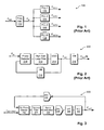
- Fig. 1 shows a conventional architecture 100 used by many ATE systems for synthesizing precise periodic signals.
- the architecture 100 includes a frequency generator 110, such as a DDS (direct digital synthesizer).
- the frequency generator 110 receives a programming value F REF and generates an analog signal having a frequency F IN , which is proportional to F REF .
- the signal having frequency F IN is then fed to one or more phase-locked loops 112-118.
- Each phase-locked loop 112-118 produces a respective output signal having a frequency F OUT that is proportional to F IN .
- the architecture 100 thus provides a way of generating numerous signals of different frequencies, but which are all derived from a common frequency, F IN .
- Fig. 2 shows a conventional phase-locked loop 200, such as may be used in the architecture 100 of Fig. 1.
- the phase-locked loop 200 receives an input signal having a frequency F IN and generates an output signal having a frequency F OUT .
- the phase-locked loop 200 is a feedback circuit having a forward path and a feedback path.
- the forward path includes a phase detector 210, a high gain loop filter 212, and a voltage-controlled oscillator (VCO) 214.
- the feedback path generally includes a first frequency divider 218. This divider in the feedback path has the effect of multiplying the output frequency.
- a second frequency divider 216 may optionally be provided outside the feedback loop for dividing the output frequency.
- the phase detector 210 receives two input signals: the input signal at frequency F IN and a feedback signal at frequency F OUT /M.
- the phase detector 210 includes circuitry for comparing the phase of its input signals to produce an output signal proportional to the difference in phase between its input signals. If properly stabilized, the action of the feedback loop drives this phase difference to zero.
- the loop filter 212 smoothes the output of the phase detector 210 and generally rolls off the gain of the loop to establish stability.
- the VCO 214 converts the output of the loop filter into a sinusoid to produce F OUT .
- the first divider 218 (generally a counter) divides F OUT by M to produce the feedback signal.
- the second divider 216 if one is provided, divides F OUT by N.
- the overall closed loop frequency gain of the phase-locked loop 200 is therefore M/N.
- the phase-locked loop 200 introduces noise, which appears as timing jitter on synthesized output signals.
- the noise originates from several sources.
- the high-gain loop filter 212 introduces noise. It also amplifies noise generated internally and from other sources.
- the phase detector 210, VCO 214, first divider 218, and second divider 216 of the phase-locked loop 200 also add substantial noise.
- the divider 218 of the phase-locked loop 200 directly reduces the phase-locked loop's open loop gain. It is generally desirable for the divider ratio M to be large, to provide fine control over output frequency. However, the larger the value of M, the greater the reduction in open loop gain. As open loop gain is decreased, the accuracy and speed of the phase-locked loop 200 are correspondingly reduced.
- a phase detector generates a digital phase error responsive to a difference in phase between a digitally synthesized reference signal and a sampled periodic signal.
- the phase detector is used as a building block for constructing a frequency synthesizer, and the digitally synthesized reference signal is made variable to provide a wide range of output frequencies.
- Frequency synthesizers employing the phase detector may be used in electronic systems, such as ATE, for generating periodic waveforms.
- Fig. 3 shows an illustrative embodiment of a frequency synthesizer 300 according to the invention.
- the synthesizer 300 has an input for receiving input data indicative of a frequency and phase (F REF , ⁇ REF ) ⁇
- the synthesizer 300 has an output for generating an output signal F OUT .
- the frequency and phase of F OUT are determined by the input data.
- the synthesizer 300 is a feedback circuit having a forward path and a feedback path.
- the forward path includes a digital phase detector 312, a digital loop filter 314, a sigma-delta modulator 316, a DAC (digital-to-analog converter) 318, an analog filter 320, and a VCO (voltage-controlled oscillator) 322.
- the feedback path includes an ADC (analog-to-digital converter) 310.
- the digital phase detector 312 has a first input for receiving the input data (F REF , ⁇ REF ) and a second input for receiving a digital feedback signal.
- the digital phase detector 312 preferably generates a reference frequency having frequency F REF and phase ⁇ REF .
- the digital phase detector compares the reference signal with the feedback signal to generate a digital output signal indicative of the cumulative phase difference between the reference signal and the feedback signal. This is not unlike the manner in which a conventional phase detector produces a phase error proportional to a phase difference between its input signals.
- the digital loop filter 314 preferably amplifies the digital output signal from the digital phase detector.
- the digital loop filter 314 also preferably provides filtering to limit the bandwidth of the feedback loop and reduce noise.
- the sigma-delta modulator 316 is of a conventional type. It generates an output signal having a lesser number of bits than its input signal, but systematically adds content to its output signal at an elevated sampling rate to effectively regain the lost resolution.
- the DAC 318 converts the signal at the output of the sigma-delta modulator 316 to a discrete analog signal, and the filter 320 smoothes the output of the DAC 318. This includes averaging the high frequency content added by the sigma-delta modulator 316.
- the filter 320 is preferably a low-pass filter. The filter preferably has a bandwidth that is much higher than the bandwidth of the feedback loop, so that it does not affect the stability of the feedback loop.
- the output of the filter 320 is fed to the input of the VCO 322, which generates F OUT .
- the ADC 310 digitizes F OUT and passes the digitized signal (i.e., the feedback signal) back to the second input of the digital phase detector 312.
- the frequency synthesizer 300 provides numerous advantages. Because the synthesizer 300 does not require a frequency divider (such as divider 218), an analog high-gain loop filter (such as 212), or an analog phase detector (such as 210), noise from these sources is avoided. In addition, the synthesizer 300 manages its signals in digital form up to the input of the DAC 318.
- a frequency divider such as divider 2128
- an analog high-gain loop filter such as 212
- an analog phase detector such as 210
- the DAC 318 and the ADC 310 add noise to the synthesizer 300.
- the amount of noise these elements add can be kept low through the use of accurate converters and by the filtering operation of the feedback loop.
- the digital loop filter 314 is preferably programmable to selectively attenuate noise components. For example, if the ADC is known to generate a noise spur at 500 KHz, the digital loop filter 314 can be designed to have a gain of zero, or substantially zero, at 500 KHz, thus preventing the 500 KHz spur from appearing at the output of the synthesizer. Given the flexibility with which digital filters can be designed, particularly FIR (Finite Impulse Response) filters, frequency "zeroes" can be added to the transfer function of the digital loop filter 314 as needed for an arbitrary number of noise frequencies from any source. Preferably, the transfer function of the digital loop filter 314 is field programmable to accommodate particular noise characteristics of any target application.
- FIR Finite Impulse Response
- the synthesizer 300 is preferably implemented on a circuit board assembly that includes a combination of digital and analog components.
- the digital phase detector 312, digital loop filter 314, and sigma-delta modulator 316 are provided together in a single digital component, such as an FPGA (Field Programmable Gate Array) or an ASIC (Application Specific Integrated Circuit). This is not required, however. Alternatively, they can be provided separately, or in the form of discrete logic. Some components can be provided in separate FPGAs, ASICs, or discrete logic, and others can be provided together.
- the digital phase detector 312, digital loop filter 314, and sigma-delta modulator 316 can also be implemented in software that runs on a computer processor.
- the ADC 310 preferably has a resolution of at least 14 bits and a sampling rate of 100 MSa/s. This is not required, however.
- the type of converter e.g., sigma-delta, successive approximation, etc.
- the ADC 310 may be implemented as a bandpass sigma-delta converter.
- the DAC 318 preferably has a high resolution (e.g., 16-24 bits). Again, the type of converter is not critical to the invention.
- Fig. 4 shows a suitable digital phase detector for the synthesizer 300 according to an embodiment of the invention.
- the first input of the digital phase detector is coupled to a digital oscillator 414, and the second input of the digital phase detector is coupled to a down-converter 410.
- the digital oscillator 414 Based upon the input data (F REF , ⁇ REF ), the digital oscillator 414 synthesizes a digital reference signal having frequency a F OSC and a phase ⁇ OSC .
- F OSC is preferably equal to F REF
- ⁇ OSC is preferably equal to ⁇ REF .
- the digital reference signal is preferably a quadrature reference signal, i.e., it is provided in two parts that represent two sinusoids separated by a phase difference of 90-degrees.
- a first part of the quadrature reference signal is designated as a cosine and a second part is designated as a sine. Therefore, the first part of the quadrature reference signal has the form Cos(2 ⁇ F OSC t + ⁇ OSC ) and the second part has the form Sin(2 ⁇ F OSC t + ⁇ OSC ).
- the quadrature reference signal is provided to the down-converter 510, whereupon it is mixed with the feedback signal.
- the feedback signal can be regarded more generally as a sampled periodic signal having the form Cos(2 ⁇ F IN t + ⁇ IN ).
- the down-converter 410 produces a difference signal in response to the sampled periodic signal and quadrature reference signal.
- the difference signal is preferably a quadrature signal having two parts: one part having substantially the form Cos[2 ⁇ (F IN -F OSC )t + ⁇ IN - ⁇ OSC ], and the other part having substantially the form Sin[2 ⁇ (F IN - F OSC )t + ⁇ IN - ⁇ OSC ]. Therefore, the frequency of the quadrature difference signal equals the difference between the input and oscillator frequencies, F IN - F OSC , and the phase of the quadrature difference signal equals the difference between the input and oscillator phases, ⁇ IN - ⁇ OSC .
- a Hilbert filter 612 generates a 90-degree phase-shifted version of the sampled periodic signal.
- a delay unit 610 accounts for any fixed propagation delay in the Hilbert filter 612. The output of the delay unit 610 and the output of the Hilbert filter 612 together form a quadrature version of the sampled periodic signal.
- a demodulator 614 demodulates the quadrature version of the sampled periodic signal with the quadrature reference signal to product the quadrature difference signal.
- Fig. 7 shows a far simpler approach.
- the sampled periodic signal is respectively provided to first and second multipliers 710 and 712.
- the first multiplier 710 multiplies the sampled periodic signal by the first part of the quadrature reference signal
- the second multiplier 712 multiplies the sampled periodic signal by the second part of the quadrature reference signal.
- Each multiplication generates sum and difference components.
- First and second digital low-pass filters 714 and 716 respectively filter the outputs of the first and second multipliers 710 and 712 to remove the sum components and pass the difference components. These difference components form the quadrature difference signal.
- the quadrature difference signal is provided to a phase extractor 416.
- the phase extractor 416 generates a cumulative phase difference represented by the quadrature difference signal.
- the phase extractor 416 performs an ATAN2 function.
- ATAN2 generates a 4-quadrant inverse tangent of a quotient of two inputs. Where the two inputs to ATAN2 are a sine and a cosine of the same angle, ⁇ , ATAN2 [sin( ⁇ ), cos( ⁇ )] is simply the angle, ⁇ . Therefore, ATAN2 of the two parts of the quadrature difference signal evaluates to [2 ⁇ (F IN - F OSC )t + ⁇ IN - ⁇ OSC ].
- This value corresponds to the cumulative phase difference between the output of the digital oscillator 514 and the sampled periodic signal. If F IN , F OSC , ⁇ IN and ⁇ OSC are constant, the values described by the cumulative phase difference take the form of a straight line over time.
- the cumulative phase difference produced by the phase extractor 416 provides a digital phase error, which is not unlike the analog phase error generated by the analog phase detector 210 of the prior art.
- a phase ⁇ ADJ may be added to or subtracted from the cumulative phase difference, via a summer 420, to adjust the phase error passed to other components of the synthesizer 300. Adding or subtracting phase via the summer 420 has the effect of shifting the phase of the synthesizer's output signal, F OUT .
- the digital oscillator 414 should be able to generate the quadrature reference signal with precision.
- F OSC should substantially equal the frequency specified by F REF (nominally, F OSC and F REF are equal) and ⁇ OSC must substantially equal the phase specified by ⁇ REF (nominally, ⁇ OSC and ⁇ REF are equal). This requirement places significant demands on the digital oscillator 414, as it is required to produce precise values of the quadrature reference signal on the fly and at the requisite sampling rate.
- the digital oscillator 414 can employ a look-up table for generating the quadrature reference signal.
- the look-up table associates pre-stored values of the quadrature reference signal with successive cycles of the sample clock. The digital oscillator can thus generate the quadrature reference signal simply by cycling through values stored its look-up table.
- Fig. 5 shows an alternative embodiment of the digital phase detector 312.
- the down-converter 510, phase extractor 516, and summer 520 of Fig. 5 are substantially the same as the down-converter 410, phase extractor 416, and summer 420 of Fig. 4.
- Fig. 5 also includes a calculation unit 512, an accumulator 518, and a second summer 522.
- the calculation unit 512 divides the input data (F REF , ⁇ REF ) into two parts, a primary part and a secondary part.
- the primary part (F OSC , ⁇ OSC ) represents an approximation of the reference signal (F REF , ⁇ REF ) that the digital oscillator 514 can readily generate, such as by using a look-up table.
- the secondary part ( ⁇ RES ) represents a residual phase value, i.e., the error in the above approximation.
- the accumulator 518 accumulates (i.e., adds to its own contents) values of ⁇ RES on each cycle of F S .
- the output of the phase extractor 516 does not account for the secondary part of the input data.
- the summer 522 corrects this output by subtracting the output of the accumulator 518 from the output of the phase extractor 516.
- the output of the summer 522 thus accounts for both the primary and secondary parts of the input data, and produces an accurate representation of phase error between the sampled periodic signal and the reference (i.e., F REF , ⁇ REF ).
- the reference data (F REF , ⁇ REF ) is preferably variable.
- the reference data is preferably programmable for establishing different output frequencies.
- the values of the integers K and L are preferably updated each time a new value of reference data is programmed.
- K is preferably made as large as practicable.
- K and L may be computed manually, or may be generated by software, firmware, or hardware based upon the desired output frequency and the sampling rate.
- phase error is updated at a high frequency, such as once per cycle of the sample clock.
- phase error is provided with exceedingly high resolution.
- ⁇ RES is managed independently of the primary part of the reference frequency, a large number of bits of numerical precision can be applied to ⁇ RES .
- the contribution of ⁇ RES to the overall phase error can be made exceedingly small by increasing the number of cycles of F OSC (i.e., the value of K) that are stored in the look-up table used to implement the digital oscillator 514.
- Fig. 8 shows a process according to an embodiment of the invention for measuring a cumulative phase difference between a periodic sampled signal and a digital oscillatory reference signal.
- both the digital phase detector of Fig. 4 and the digital phase detector of Fig. 5 can be arranged to conduct this process.
- Fig. 9 shows a process according to another embodiment of the invention for measuring a cumulative phase difference between a periodic sampled signal and a digital oscillatory reference signal.
- the digital phase detector of Fig. 5 can be arranged to conduct this process.
- Fig. 10 shows an application of frequency synthesizers of the type shown in Fig. 3.
- An automatic test system 1012 is controlled by a host computer 1010 for testing a DUT (device under test) 1040.
- the automatic test system 1012 includes instruments, such as an analog instrument 1020, a digitizer 1022, and an arbitrary waveform generator (AWG) 1024.
- the automatic test system 1012 may also include a plurality of digital electronic channels, shown generally as digital pins 1026, 1028, and 1030. The digital electronic channels are arranged for sourcing and sensing digital signals.
- the automatic test system 1012 includes a plurality of frequency synthesizers 1016a-g.
- These synthesizers are of the same general type as that shown in Fig. 3.
- the synthesizers 1016a-g each receive a clock signal, F S , from a system clock 1014. They also each receive respective input data (F REF , ⁇ REF ) for specifying desired output frequencies and phases.
- the frequency synthesizers 1016a-g each generate a respective periodic output signal. These output signals can be provided to the instruments 1020, 1022, and 1024, which may require frequency references or clocks for their normal operation.
- the output signals can also be used as clocks for controlling the digital pins 1026, 1028, and 1030.
- a frequency synthesizer can be used as input to a pattern generator 1018.
- the pattern generator 1018 can work in conjunction with frequency synthesizers for causing the digital pins to source and/or sense digital signals with specified formatting and at precisely controlled instants of time.
- Figs. 4 and 5 have been shown and described for use in connection with frequency synthesizers, such as the one shown in Fig. 3.
- these digital phase detectors may be used in any application to measure a phase difference between an input signal and a reference.
- the synthesizer of Fig. 3 includes a digital loop filter 314.
- an analog loop filter similar to the filter 212, may be inserted at the output of the DAC 318, and the digital loop filter 314 may be omitted.
- the synthesizer 300 includes a sigma-delta modulator 316.
- the sigma-delta modulator may be omitted.
- the words “comprising,” having,” and “including,” as well as grammatical variations of these words do not signal closed groups of elements, but rather open-ended groups that may contain additional elements.
- the word “coupling” and grammatical variations thereof do not require a direct connection between elements, but designate connections that may be direct or indirect. Therefore, elements may be connected between elements that are “coupled” together.
Landscapes
- Physics & Mathematics (AREA)
- Engineering & Computer Science (AREA)
- General Physics & Mathematics (AREA)
- General Engineering & Computer Science (AREA)
- Nonlinear Science (AREA)
- Power Engineering (AREA)
- Stabilization Of Oscillater, Synchronisation, Frequency Synthesizers (AREA)
- Manipulation Of Pulses (AREA)
- Measuring Phase Differences (AREA)
Applications Claiming Priority (2)
| Application Number | Priority Date | Filing Date | Title |
|---|---|---|---|
| US817780 | 2004-04-02 | ||
| US10/817,780 US7061276B2 (en) | 2004-04-02 | 2004-04-02 | Digital phase detector |
Publications (2)
| Publication Number | Publication Date |
|---|---|
| EP1584929A2 true EP1584929A2 (de) | 2005-10-12 |
| EP1584929A3 EP1584929A3 (de) | 2006-10-04 |
Family
ID=34912677
Family Applications (1)
| Application Number | Title | Priority Date | Filing Date |
|---|---|---|---|
| EP05002023A Withdrawn EP1584929A3 (de) | 2004-04-02 | 2005-02-01 | Phasendetektor mit Digitaloszillator |
Country Status (5)
| Country | Link |
|---|---|
| US (2) | US7061276B2 (de) |
| EP (1) | EP1584929A3 (de) |
| JP (3) | JP2005295544A (de) |
| CN (1) | CN100481711C (de) |
| TW (1) | TWI292656B (de) |
Cited By (4)
| Publication number | Priority date | Publication date | Assignee | Title |
|---|---|---|---|---|
| EP1873919A1 (de) * | 2006-06-29 | 2008-01-02 | Nihon Dempa Kogyo Co., Ltd. | Frequenzsynthesizer |
| US7642862B2 (en) | 2006-11-17 | 2010-01-05 | Zarlink Semiconductor Inc. | Digital phase locked loop |
| DE102016115785A1 (de) * | 2016-08-25 | 2018-03-01 | Infineon Technologies Ag | Integrierte RF-Schaltung mit Möglichkeit zum Testen von Phasenrauschen |
| CN109324215A (zh) * | 2018-09-21 | 2019-02-12 | 北京无线电计量测试研究所 | 一种基于dds的标准相位产生方法和装置 |
Families Citing this family (48)
| Publication number | Priority date | Publication date | Assignee | Title |
|---|---|---|---|---|
| DE10215087B4 (de) * | 2002-04-05 | 2004-08-19 | Infineon Technologies Ag | Verfahren und Vorrichtung zur Phasendetektion |
| DE102004006995B4 (de) * | 2004-02-12 | 2007-05-31 | Infineon Technologies Ag | Digitaler Phasenregelkreis für Sub-µ-Technologien |
| US7340219B2 (en) * | 2004-02-24 | 2008-03-04 | Texas Instruments Incorporated | Method and system for multisite RF transceiver testing |
| DE102004032130B4 (de) * | 2004-07-01 | 2010-12-16 | Krohne Messtechnik Gmbh | Frequenzsynthesizer und Verfahren zum Betrieb eines Frequenzsynthesizers |
| EP1875610B1 (de) * | 2005-04-18 | 2011-03-30 | Nxp B.V. | Schaltungsanordnung, insbesondere phasenregelkreis, sowie entsprechendes verfahren |
| US7711328B1 (en) | 2005-06-29 | 2010-05-04 | Xilinx, Inc. | Method of and circuit for sampling a frequency difference in an integrated circuit |
| US7635997B1 (en) * | 2005-06-29 | 2009-12-22 | Xilinx, Inc. | Circuit for and method of changing a frequency in a circuit |
| US7173462B1 (en) * | 2005-10-27 | 2007-02-06 | Mediatek Inc. | Second order delay-locked loop for data recovery |
| US7443251B2 (en) * | 2005-12-15 | 2008-10-28 | International Business Machines Corporation | Digital phase and frequency detector |
| US7847641B2 (en) * | 2005-12-15 | 2010-12-07 | International Business Machines Corporation | Digital phase and frequency detector |
| US7345549B2 (en) * | 2006-02-28 | 2008-03-18 | Teradyne, Inc. | Phase locking on aliased frequencies |
| US7680227B2 (en) * | 2006-03-02 | 2010-03-16 | Broadcom Corporation | Method and system for filter calibration using fractional-N frequency synthesized signals |
| US7683851B2 (en) * | 2007-03-19 | 2010-03-23 | Broadcom Corporation | Method and system for using a single transformer for FM transmit and FM receive functions |
| DE102007016642B4 (de) * | 2007-04-05 | 2015-12-17 | Austriamicrosystems Ag | Elektromechanisches System und Verfahren zum Betrieb eines elektromechanischen Systems |
| WO2009014535A1 (en) * | 2007-07-23 | 2009-01-29 | Teradyne, Inc. | Phase locking on aliased frequencies |
| US20090085674A1 (en) * | 2007-09-28 | 2009-04-02 | Ahmadreza Rofougaran | Method and system for signal generation via a pll with digital phase detection |
| US20090085678A1 (en) * | 2007-09-28 | 2009-04-02 | Ahmadreza Rofougaran | Method and system for signal generation via a digitally controlled oscillator |
| US7724096B2 (en) * | 2007-09-28 | 2010-05-25 | Broadcom Corporation | Method and system for signal generation via a PLL with undersampled feedback |
| CN101842987B (zh) * | 2007-11-12 | 2013-11-06 | 松下电器产业株式会社 | Pll电路和使用该pll电路的角速度传感器 |
| US20090243741A1 (en) * | 2008-03-27 | 2009-10-01 | Ahmadreza Rofougaran | Method and system for processing signals via an oscillator load embedded in an integrated circuit (ic) package |
| US20090243740A1 (en) * | 2008-03-27 | 2009-10-01 | Ahmadreza Rofougaran | Method and system for reduced jitter signal generation |
| US8086190B2 (en) * | 2008-03-27 | 2011-12-27 | Broadcom Corporation | Method and system for reconfigurable devices for multi-frequency coexistence |
| PL2149990T3 (pl) * | 2008-07-29 | 2011-10-31 | Siemens Ag | System, zwłaszcza do digitalizacji okresowego sygnału z ciągłym czasem i ciągłą wartością, ze stałą z góry określoną liczbą wartości próbkowania przypadającą na jeden okres |
| TW201230733A (en) * | 2011-01-12 | 2012-07-16 | Tsung-Hsien Lin | Receiver |
| KR20120125096A (ko) * | 2011-05-06 | 2012-11-14 | 삼성전자주식회사 | 디지털 제어 발진기를 포함하는 위상동기루프 회로 |
| US8862648B2 (en) | 2011-05-24 | 2014-10-14 | Taiwan Semiconductor Manufacturing Company, Ltd. | Fast filter calibration apparatus |
| US8664986B2 (en) | 2011-07-28 | 2014-03-04 | Intel Corporation | System, method and emulation circuitry useful for adjusting a characteristic of a periodic signal |
| JP2013207737A (ja) * | 2012-03-29 | 2013-10-07 | Fujitsu Ltd | 位相検出回路、半導体装置及び位相検出方法 |
| CN103475363A (zh) * | 2013-09-04 | 2013-12-25 | 苏州苏尔达信息科技有限公司 | 一种二元相位比较器数字锁相环电路 |
| JP2015215684A (ja) | 2014-05-08 | 2015-12-03 | 富士ゼロックス株式会社 | 情報処理装置及び情報処理プログラム |
| US9246499B2 (en) * | 2014-05-21 | 2016-01-26 | Robert Bosch Gmbh | Digital phase lock loop circuit including finite impulse response filtering to reduce aliasing of quantization noise |
| JP6382342B2 (ja) * | 2014-12-08 | 2018-08-29 | 古野電気株式会社 | 基準信号発生装置 |
| US10126884B2 (en) | 2014-12-22 | 2018-11-13 | Synaptics Incorporated | Asynchronous interference detection in a capacitive sensing system |
| US9755766B2 (en) * | 2015-12-07 | 2017-09-05 | Teradyne, Inc. | Front end module for automatic test equipment |
| JP6862900B2 (ja) * | 2017-02-22 | 2021-04-21 | セイコーエプソン株式会社 | 回路装置、物理量測定装置、電子機器及び移動体 |
| US11095295B2 (en) | 2018-06-26 | 2021-08-17 | Silicon Laboratories Inc. | Spur cancellation for spur measurement |
| US10659060B2 (en) | 2018-09-27 | 2020-05-19 | Silicon Laboratories Inc. | Spur cancellation with adaptive frequency tracking |
| US10680622B2 (en) * | 2018-09-27 | 2020-06-09 | Silicon Laboratories Inc. | Spur canceller with multiplier-less correlator |
| US10819353B1 (en) | 2019-10-04 | 2020-10-27 | Silicon Laboratories Inc. | Spur cancellation in a PLL system with an automatically updated target spur frequency |
| US11038521B1 (en) | 2020-02-28 | 2021-06-15 | Silicon Laboratories Inc. | Spur and quantization noise cancellation for PLLS with non-linear phase detection |
| CN111289864B (zh) * | 2020-04-02 | 2023-02-28 | 全球能源互联网研究院有限公司 | 一种局部放电高频电流抗干扰检测系统及方法 |
| US11316522B2 (en) | 2020-06-15 | 2022-04-26 | Silicon Laboratories Inc. | Correction for period error in a reference clock signal |
| CN112710890B (zh) * | 2020-12-15 | 2024-02-27 | 特变电工西安电气科技有限公司 | 一种单相正弦交流相量实时计算方法及装置 |
| CN113406453B (zh) * | 2021-06-30 | 2023-06-23 | 平顶山学院 | 一种基于mcu的prpd/prps图谱数据处理方法及检测装置 |
| US11563444B1 (en) | 2021-09-09 | 2023-01-24 | Textron Systems Corporation | Suppressing spurious signals in direct-digital synthesizers |
| KR102833443B1 (ko) * | 2021-09-13 | 2025-07-10 | 삼성전자주식회사 | 패턴 생성기 및 이를 포함하는 내장 자체 시험 장치 |
| CN114430262B (zh) * | 2022-01-14 | 2023-03-28 | 中星联华科技(北京)有限公司 | 适用于码型发生器的相位调节装置、系统及方法 |
| KR102888889B1 (ko) * | 2023-07-05 | 2025-11-21 | 주식회사 에픽솔루션 | 프로그램어블 위상 변위기를 이용한 주파수 합성기 |
Family Cites Families (10)
| Publication number | Priority date | Publication date | Assignee | Title |
|---|---|---|---|---|
| US4090145A (en) * | 1969-03-24 | 1978-05-16 | Webb Joseph A | Digital quadrature demodulator |
| US4156204A (en) * | 1976-06-03 | 1979-05-22 | Motorola, Inc. | Voltage controlled oscillator with frequency and phase control loop |
| US5444420A (en) * | 1994-09-29 | 1995-08-22 | Harris Corporation | Numerically controlled phase lock loop synthesizer/modulator and method |
| KR100217361B1 (ko) * | 1997-06-30 | 1999-09-01 | 김영환 | Vsb 디지털 복조기 |
| CN1178485C (zh) * | 1997-10-31 | 2004-12-01 | 汤姆森许可公司 | 高清晰度电视残留边带接收机 |
| CN1157943C (zh) * | 1999-07-16 | 2004-07-14 | 汤姆森许可公司 | 高清晰度电视接收机中帮助载波获取的可选增益调整 |
| US6252464B1 (en) * | 1999-10-06 | 2001-06-26 | Cubic Defense Systems, Inc. | Numerically-controlled nyquist-boundary hopping frequency synthesizer |
| US6807134B2 (en) * | 1999-12-28 | 2004-10-19 | Matsushita Electric Industrial Co., Ltd. | Asymmetry detection apparatus, jitter detection apparatus, and recording/reproduction apparatus |
| US6603362B2 (en) * | 2000-03-14 | 2003-08-05 | Intersil Americas Inc. | Subsampling digitizer-based frequency synthesizer |
| DE10205044A1 (de) * | 2002-02-07 | 2003-08-21 | Philips Intellectual Property | Digitaler Phase Locked Loop |
-
2004
- 2004-04-02 US US10/817,780 patent/US7061276B2/en not_active Expired - Lifetime
-
2005
- 2005-02-01 EP EP05002023A patent/EP1584929A3/de not_active Withdrawn
- 2005-02-22 TW TW094105194A patent/TWI292656B/zh not_active IP Right Cessation
- 2005-03-24 JP JP2005086535A patent/JP2005295544A/ja active Pending
- 2005-03-29 CN CNB2005100593722A patent/CN100481711C/zh not_active Expired - Lifetime
-
2006
- 2006-05-09 US US11/430,663 patent/US7432751B2/en not_active Expired - Lifetime
-
2010
- 2010-03-15 JP JP2010057327A patent/JP5154594B2/ja not_active Expired - Lifetime
- 2010-03-15 JP JP2010057324A patent/JP5165712B2/ja not_active Expired - Lifetime
Cited By (8)
| Publication number | Priority date | Publication date | Assignee | Title |
|---|---|---|---|---|
| EP1873919A1 (de) * | 2006-06-29 | 2008-01-02 | Nihon Dempa Kogyo Co., Ltd. | Frequenzsynthesizer |
| US7508281B2 (en) | 2006-06-29 | 2009-03-24 | Nihon Dempa Kogyo., Ltd | Frequency synthesizer |
| US7642862B2 (en) | 2006-11-17 | 2010-01-05 | Zarlink Semiconductor Inc. | Digital phase locked loop |
| DE102016115785A1 (de) * | 2016-08-25 | 2018-03-01 | Infineon Technologies Ag | Integrierte RF-Schaltung mit Möglichkeit zum Testen von Phasenrauschen |
| US10090939B2 (en) | 2016-08-25 | 2018-10-02 | Infineon Technologies Ag | Integrated RF circuit with phase-noise test capability |
| US10205541B2 (en) | 2016-08-25 | 2019-02-12 | Infineon Technologies Ag | Integrated RF circuit with phase-noise test capability |
| CN109324215A (zh) * | 2018-09-21 | 2019-02-12 | 北京无线电计量测试研究所 | 一种基于dds的标准相位产生方法和装置 |
| CN109324215B (zh) * | 2018-09-21 | 2022-04-19 | 北京无线电计量测试研究所 | 一种基于dds的标准相位产生方法和装置 |
Also Published As
| Publication number | Publication date |
|---|---|
| CN1677844A (zh) | 2005-10-05 |
| US20060202733A1 (en) | 2006-09-14 |
| JP2005295544A (ja) | 2005-10-20 |
| US7432751B2 (en) | 2008-10-07 |
| TW200534590A (en) | 2005-10-16 |
| JP2010141933A (ja) | 2010-06-24 |
| CN100481711C (zh) | 2009-04-22 |
| TWI292656B (en) | 2008-01-11 |
| JP2010161797A (ja) | 2010-07-22 |
| JP5154594B2 (ja) | 2013-02-27 |
| EP1584929A3 (de) | 2006-10-04 |
| JP5165712B2 (ja) | 2013-03-21 |
| US20050218997A1 (en) | 2005-10-06 |
| US7061276B2 (en) | 2006-06-13 |
Similar Documents
| Publication | Publication Date | Title |
|---|---|---|
| US7061276B2 (en) | Digital phase detector | |
| US6380811B1 (en) | Signal generator, and method | |
| Kumm et al. | An FPGA-based linear all-digital phase-locked loop | |
| US6636122B2 (en) | Analog frequency locked loop with digital oversampling feedback control and filter | |
| JP3456977B2 (ja) | Nmr分光計を動作させる方法 | |
| US3984771A (en) | Accurate digital phase/frequency extractor | |
| CN101765974B (zh) | 混叠频率的锁相 | |
| CN117914308B (zh) | 分子时钟装置、分子时钟频率控制方法和电子设备 | |
| CN113839670A (zh) | 一种高性能频率改正方法、频率改正系统和改进的锁相环 | |
| CN109391267A (zh) | 使用带adcs和dac的数字plls时的抖动减少技术 | |
| US20080231254A1 (en) | Spectrum analyzer, spectrum analysis method and recording medium | |
| US20070019768A1 (en) | Sampling device and sampling method | |
| JPS58174861A (ja) | アナログ・デジタル変換器の特性測定装置 | |
| Simrock et al. | Considerations for the choice of the intermediate frequency and sampling rate for digital RF control | |
| JPH07209351A (ja) | スペクトラム・アナライザ用局部発振器 | |
| Arablu et al. | Synchronous radio-frequency FM signal generator using direct digital synthesizers | |
| US11105837B2 (en) | Frequency multiplying device | |
| CN101416392B (zh) | Pll装置 | |
| US9654124B1 (en) | Coherent signal source | |
| TW595106B (en) | Digital frequency synthesizer based pLL | |
| US20210336625A1 (en) | Method and Apparatus for Generating Output Frequency Locked to Input Frequency | |
| JP6794784B2 (ja) | 周波数シンセサイザー | |
| JPH07183804A (ja) | 周波数シンセサイザ | |
| JPH0261803B2 (de) | ||
| JPH08101747A (ja) | シーケンシャルサンプリングシステム |
Legal Events
| Date | Code | Title | Description |
|---|---|---|---|
| PUAI | Public reference made under article 153(3) epc to a published international application that has entered the european phase |
Free format text: ORIGINAL CODE: 0009012 |
|
| AK | Designated contracting states |
Kind code of ref document: A2 Designated state(s): AT BE BG CH CY CZ DE DK EE ES FI FR GB GR HU IE IS IT LI LT LU MC NL PL PT RO SE SI SK TR |
|
| AX | Request for extension of the european patent |
Extension state: AL BA HR LV MK YU |
|
| PUAL | Search report despatched |
Free format text: ORIGINAL CODE: 0009013 |
|
| RIC1 | Information provided on ipc code assigned before grant |
Ipc: H03D 13/00 20060101ALI20060822BHEP Ipc: H03L 7/085 20060101ALI20060822BHEP Ipc: H03L 7/16 20060101ALI20060822BHEP Ipc: G01R 25/00 20060101AFI20050728BHEP |
|
| AK | Designated contracting states |
Kind code of ref document: A3 Designated state(s): AT BE BG CH CY CZ DE DK EE ES FI FR GB GR HU IE IS IT LI LT LU MC NL PL PT RO SE SI SK TR |
|
| AX | Request for extension of the european patent |
Extension state: AL BA HR LV MK YU |
|
| 17P | Request for examination filed |
Effective date: 20070315 |
|
| AKX | Designation fees paid |
Designated state(s): DE FR GB IE IT |
|
| STAA | Information on the status of an ep patent application or granted ep patent |
Free format text: STATUS: THE APPLICATION IS DEEMED TO BE WITHDRAWN |
|
| 18D | Application deemed to be withdrawn |
Effective date: 20090901 |