EP1582360A2 - Thermokopf mit zwischen Kühlkörperplatte und Kopfsubstrat aufgetragenem Klebstof und Herstellungsverfahren dafür - Google Patents
Thermokopf mit zwischen Kühlkörperplatte und Kopfsubstrat aufgetragenem Klebstof und Herstellungsverfahren dafür Download PDFInfo
- Publication number
- EP1582360A2 EP1582360A2 EP05006022A EP05006022A EP1582360A2 EP 1582360 A2 EP1582360 A2 EP 1582360A2 EP 05006022 A EP05006022 A EP 05006022A EP 05006022 A EP05006022 A EP 05006022A EP 1582360 A2 EP1582360 A2 EP 1582360A2
- Authority
- EP
- European Patent Office
- Prior art keywords
- head substrate
- heat
- dissipation plate
- wide
- heating resistors
- Prior art date
- Legal status (The legal status is an assumption and is not a legal conclusion. Google has not performed a legal analysis and makes no representation as to the accuracy of the status listed.)
- Granted
Links
- 239000000758 substrate Substances 0.000 title claims abstract description 130
- 230000017525 heat dissipation Effects 0.000 title claims abstract description 89
- 239000000853 adhesive Substances 0.000 title claims abstract description 63
- 230000001070 adhesive effect Effects 0.000 title claims abstract description 63
- 238000004519 manufacturing process Methods 0.000 title claims description 10
- 238000010438 heat treatment Methods 0.000 claims abstract description 84
- XAGFODPZIPBFFR-UHFFFAOYSA-N aluminium Chemical compound [Al] XAGFODPZIPBFFR-UHFFFAOYSA-N 0.000 claims description 49
- 229910052782 aluminium Inorganic materials 0.000 claims description 49
- 238000007789 sealing Methods 0.000 claims description 15
- 239000010931 gold Substances 0.000 claims description 12
- 238000005304 joining Methods 0.000 claims description 9
- PCHJSUWPFVWCPO-UHFFFAOYSA-N gold Chemical compound [Au] PCHJSUWPFVWCPO-UHFFFAOYSA-N 0.000 claims description 4
- 229910052737 gold Inorganic materials 0.000 claims description 4
- 238000000034 method Methods 0.000 claims description 2
- 239000010410 layer Substances 0.000 description 21
- 238000005259 measurement Methods 0.000 description 19
- 239000012790 adhesive layer Substances 0.000 description 8
- 229920005989 resin Polymers 0.000 description 8
- 239000011347 resin Substances 0.000 description 8
- 230000008602 contraction Effects 0.000 description 6
- 230000004888 barrier function Effects 0.000 description 5
- 229910018170 Al—Au Inorganic materials 0.000 description 3
- 238000005452 bending Methods 0.000 description 3
- 239000011241 protective layer Substances 0.000 description 3
- XUIMIQQOPSSXEZ-UHFFFAOYSA-N Silicon Chemical compound [Si] XUIMIQQOPSSXEZ-UHFFFAOYSA-N 0.000 description 2
- 229910045601 alloy Inorganic materials 0.000 description 2
- 239000000956 alloy Substances 0.000 description 2
- 239000003822 epoxy resin Substances 0.000 description 2
- 229920000647 polyepoxide Polymers 0.000 description 2
- 239000010703 silicon Substances 0.000 description 2
- 229910052710 silicon Inorganic materials 0.000 description 2
- 238000010301 surface-oxidation reaction Methods 0.000 description 2
- 238000009825 accumulation Methods 0.000 description 1
- PNEYBMLMFCGWSK-UHFFFAOYSA-N aluminium oxide Inorganic materials [O-2].[O-2].[O-2].[Al+3].[Al+3] PNEYBMLMFCGWSK-UHFFFAOYSA-N 0.000 description 1
- 229910010293 ceramic material Inorganic materials 0.000 description 1
- 238000000151 deposition Methods 0.000 description 1
- 230000002542 deteriorative effect Effects 0.000 description 1
- 238000007599 discharging Methods 0.000 description 1
- 238000005562 fading Methods 0.000 description 1
Images



Classifications
-
- B—PERFORMING OPERATIONS; TRANSPORTING
- B41—PRINTING; LINING MACHINES; TYPEWRITERS; STAMPS
- B41J—TYPEWRITERS; SELECTIVE PRINTING MECHANISMS, i.e. MECHANISMS PRINTING OTHERWISE THAN FROM A FORME; CORRECTION OF TYPOGRAPHICAL ERRORS
- B41J2/00—Typewriters or selective printing mechanisms characterised by the printing or marking process for which they are designed
- B41J2/315—Typewriters or selective printing mechanisms characterised by the printing or marking process for which they are designed characterised by selective application of heat to a heat sensitive printing or impression-transfer material
- B41J2/32—Typewriters or selective printing mechanisms characterised by the printing or marking process for which they are designed characterised by selective application of heat to a heat sensitive printing or impression-transfer material using thermal heads
- B41J2/335—Structure of thermal heads
- B41J2/33585—Hollow parts under the heater
-
- B—PERFORMING OPERATIONS; TRANSPORTING
- B41—PRINTING; LINING MACHINES; TYPEWRITERS; STAMPS
- B41J—TYPEWRITERS; SELECTIVE PRINTING MECHANISMS, i.e. MECHANISMS PRINTING OTHERWISE THAN FROM A FORME; CORRECTION OF TYPOGRAPHICAL ERRORS
- B41J2/00—Typewriters or selective printing mechanisms characterised by the printing or marking process for which they are designed
- B41J2/315—Typewriters or selective printing mechanisms characterised by the printing or marking process for which they are designed characterised by selective application of heat to a heat sensitive printing or impression-transfer material
- B41J2/32—Typewriters or selective printing mechanisms characterised by the printing or marking process for which they are designed characterised by selective application of heat to a heat sensitive printing or impression-transfer material using thermal heads
- B41J2/335—Structure of thermal heads
- B41J2/33575—Processes for assembling process heads
-
- B—PERFORMING OPERATIONS; TRANSPORTING
- B41—PRINTING; LINING MACHINES; TYPEWRITERS; STAMPS
- B41J—TYPEWRITERS; SELECTIVE PRINTING MECHANISMS, i.e. MECHANISMS PRINTING OTHERWISE THAN FROM A FORME; CORRECTION OF TYPOGRAPHICAL ERRORS
- B41J2/00—Typewriters or selective printing mechanisms characterised by the printing or marking process for which they are designed
- B41J2/315—Typewriters or selective printing mechanisms characterised by the printing or marking process for which they are designed characterised by selective application of heat to a heat sensitive printing or impression-transfer material
- B41J2/32—Typewriters or selective printing mechanisms characterised by the printing or marking process for which they are designed characterised by selective application of heat to a heat sensitive printing or impression-transfer material using thermal heads
- B41J2/335—Structure of thermal heads
- B41J2/3358—Cooling arrangements
-
- B—PERFORMING OPERATIONS; TRANSPORTING
- B41—PRINTING; LINING MACHINES; TYPEWRITERS; STAMPS
- B41J—TYPEWRITERS; SELECTIVE PRINTING MECHANISMS, i.e. MECHANISMS PRINTING OTHERWISE THAN FROM A FORME; CORRECTION OF TYPOGRAPHICAL ERRORS
- B41J2/00—Typewriters or selective printing mechanisms characterised by the printing or marking process for which they are designed
- B41J2/315—Typewriters or selective printing mechanisms characterised by the printing or marking process for which they are designed characterised by selective application of heat to a heat sensitive printing or impression-transfer material
- B41J2/32—Typewriters or selective printing mechanisms characterised by the printing or marking process for which they are designed characterised by selective application of heat to a heat sensitive printing or impression-transfer material using thermal heads
- B41J2/335—Structure of thermal heads
- B41J2/3359—Manufacturing processes
-
- B—PERFORMING OPERATIONS; TRANSPORTING
- B41—PRINTING; LINING MACHINES; TYPEWRITERS; STAMPS
- B41J—TYPEWRITERS; SELECTIVE PRINTING MECHANISMS, i.e. MECHANISMS PRINTING OTHERWISE THAN FROM A FORME; CORRECTION OF TYPOGRAPHICAL ERRORS
- B41J29/00—Details of, or accessories for, typewriters or selective printing mechanisms not otherwise provided for
- B41J29/377—Cooling or ventilating arrangements
-
- H—ELECTRICITY
- H05—ELECTRIC TECHNIQUES NOT OTHERWISE PROVIDED FOR
- H05K—PRINTED CIRCUITS; CASINGS OR CONSTRUCTIONAL DETAILS OF ELECTRIC APPARATUS; MANUFACTURE OF ASSEMBLAGES OF ELECTRICAL COMPONENTS
- H05K3/00—Apparatus or processes for manufacturing printed circuits
- H05K3/0058—Laminating printed circuit boards onto other substrates, e.g. metallic substrates
-
- H—ELECTRICITY
- H05—ELECTRIC TECHNIQUES NOT OTHERWISE PROVIDED FOR
- H05K—PRINTED CIRCUITS; CASINGS OR CONSTRUCTIONAL DETAILS OF ELECTRIC APPARATUS; MANUFACTURE OF ASSEMBLAGES OF ELECTRICAL COMPONENTS
- H05K3/00—Apparatus or processes for manufacturing printed circuits
- H05K3/38—Improvement of the adhesion between the insulating substrate and the metal
- H05K3/386—Improvement of the adhesion between the insulating substrate and the metal by the use of an organic polymeric bonding layer, e.g. adhesive
Definitions
- the present invention relates to a thermal head mounted in, for example, a thermal transfer printer, and a method for producing the same.
- a thermal head comprises a plurality of heating resistors which generate heat by electrification, and performs a printing operation by applying heat energy generated by the heating resistors to a print medium.
- a head substrate and a printed circuit board are separately provided, and an aluminum heat-dissipation plate is adhered to the lower surface of the head substrate and the lower surface of the printed circuit board.
- the heat substrate has the plurality of heating resistors, a common electrode connected in common to one ends of the plurality of heating resistors, and a plurality of individual electrodes connected to the other ends of the respective heating resistors.
- the printed circuit board has a plurality of drive elements which control the electrification of the heating resistors via the individual electrodes at the head substrate.
- thermal heads comprising heat-dissipation plates are disclosed in, for example, Japanese Unexamined Patent Application Publication Nos. 1-190467 and 11-28829 and Japanese Unexamined Utility Model Registration Application Publication No. 1-131538 (microfilm).
- the adhesive layer tends to become peeled there. This tendency becomes more noticeable as the heating temperature increases. Air tends to enter peeled areas of the adhesive layer, in which case such areas act as heat accumulators, and cause the temperature of the heating resistors to increase. Therefore, the print density of the heating resistors disposed at the ends increases, thereby resulting in inconsistencies in the print density as a whole.
- the head substrate becomes less resistant to bending.
- the head substrate becomes less resistant to bending.
- the area of the head substrate is at least 6 mm 2 . Therefore, even if the sealing resin undergoes thermal contraction, the head substrate does not tend to bend. Consequently, even if warping occurs in a plane of the head substrate, the warping is restricted within a range not affecting the print quality.
- Warping in a plane direction of the head substrate may be restricted by previously adhering the head substrate and the printed circuit board to the heat-dissipation plate, and, while an adhesive prevents the head substrate from bending, by wire-bonding and sealing the individual electrodes and drive elements.
- the individual electrodes formed of aluminum (Al) to reduce costs, and the drive elements are connected with a gold (Au) joining wire.
- the Al-Au wire bonding is carried out in an atmosphere of approximately 150°C in order to form an Al-Au alloy layer by breaking surface oxidation layers of the individual electrodes by ultrasonic vibration.
- the adhesive layer may become peeled as a result of increasing the length of the heat-dissipation plate in this high-temperature atmosphere.
- the pealed areas of the adhesive layer act as heat-accumulation layers due to air entering the peeled areas. Therefore, there are inconsistencies in the print density.
- thermo head which can be reduced in size, which can restrict warping caused by thermal strain, and which can prevent print density inconsistencies caused by peeling of an adhesive layer from occurring, and to provide a method for producing the same.
- the present invention focuses on restricting warping of a printed circuit board and a head substrate by adhering the head substrate and the printed circuit board to a heat-dissipation plate and then by carrying out a wire boding step and a sealing step, on absorbing thermal strain of the heat-dissipation plate by interposing a resilient adhesive having a sufficient thickness between the head substrate and the heat-dissipation plate, and on properly maintaining the heat-dissipation property of the heat-dissipation plate by applying the resilient adhesive to localized portions.
- a thermal head comprising a head substrate having a plurality of heating resistors which generate heat by electrification, a common electrode connected to one end of each heating resistor, and a plurality of individual electrodes connected to the other ends of the respective heating resistors, the head substrate being adhered and secured to a heat-dissipation plate.
- a wide-gap stepped portion is disposed in correspondence with at least a location of the head substrate directly below the heating resistors, the wide-gap stepped portion increasing an interval between an adhesion surface of the head substrate and an adhesion surface of the heat-dissipation plate.
- a resilient adhesive capable of absorbing thermal strain is interposed between the adhesion surface of the heat-dissipation plate and the adhesion surface of the head substrate in an adhesion plane where the wide-gap stepped portion is disposed.
- the heating resistors are disposed in a row at one end of the head substrate, and a plurality of the wide-gap stepped portions are disposed in correspondence with each end of the head substrate in a direction perpendicular to a direction of disposition of the heating resistors.
- wide-gap stepped portions are disposed in correspondence with both ends of the head substrate, it is possible to achieve contraction balance when the resilient adhesive in the wide-gap stepped portions hardens, so that the head substrate can be properly adhered to the heat-dissipation plate horizontally in a balanced manner.
- areas of portions where the head substrate is placed on the resilient adhesive in the wide-gap stepped portions are substantially the same.
- the wide-gap stepped portions are disposed directly below the heating resistors and directly below the individual electrodes. Since the temperature directly below the plurality of heating resistors is increased by heat generated by the heating resistors when the head operates, thermal strain of the heat-dissipation plate caused by the heat is properly absorbed by the resilient adhesive at the wide-gap stepped portion. In addition, since the temperature directly below the plurality of individual electrodes is high when wire bonding of the individual electrodes and drive elements is carried out, the thermal strain of the heat-dissipation plate caused by the heat is properly absorbed by the resilient adhesive at the wide-gap stepped portion.
- the thickness of the resilient adhesive at the wide-gap stepped portion may be at least 50 ⁇ m.
- the resilient adhesive has a thickness in this range, it has a resiliency which allows it to absorb thermal strain. Therefore, thermal strain of the heat-dissipation plate is allowed when the heating resistors are generating heat and when external heat is applied.
- the adhesion surface of either one of the head substrate and the heat-dissipation plate is a flat surface
- the adhesion surface of either of the other of the head substrate and the heat-dissipation plate is a bumpy surface having the wide-gap stepped portion.
- the heat-dissipation plate is practically an aluminum heat-dissipation plate.
- a method for producing a thermal head comprising the steps of providing a head substrate, a printed circuit board, and a heat-dissipation plate to which the head substrate and the printed circuit board are to be adhered and secured, the head substrate having a plurality of heating resistors which generate heat by electrification, a common electrode connected to one end of each heating resistor, and a plurality of individual electrodes connected to the other ends of the respective heating resistors, the printed circuit board having a plurality of drive elements which control the electrification to the heating resistors at the head substrate, forming a wide-gap stepped portion at a portion in an adhesion plane where the head substrate and the heat-dissipation plate are to be adhered, the wide-gap stepped portion increasing an interval between an adhesion surface of the head substrate and an adhesion surface of the heat-dissipation plate, applying a resilient adhesive capable of absorbing thermal strain in the adhesion
- the heating resistors are disposed in one row at one end of the head substrate, and a pair of the stepped portions opposing each other perpendicularly to a direction of disposition of the heating resistors are disposed.
- the head substrate is adhered to the heat-dissipation plate by placing both ends of the heat substrate, as viewed perpendicularly to the direction of disposition of the heating resistors, on the wide-gap stepped portions.
- the head substrate is adhered to the heat-dissipation plate while a location directly below the heating resistors and a location directly below the individual electrodes are situated on the wide-gap stepped portions.
- the individual electrodes at the head substrate are formed of aluminum, and the wire bonding step is performed on the individual electrodes and the drive elements at the printed circuit board with a gold joining wire.
- the present invention can provide a thermal head which can be reduced in size, which can restrict warping caused by thermal strain, and which can prevent print density inconsistencies caused by peeling of an adhesive layer from occurring, and can provide a method for producing the same.
- Fig. 1 is a sectional view of the structure of a thermal head of an embodiment of the present invention.
- a thermal head H1 comprises a head substrate 10 (shown in Fig. 2) and a printed circuit board 20, both of which are adhered to an aluminum heat-dissipation plate 1.
- a glazed layer 12 As shown in Figs. 1 and 2, in the head substrate 10, a glazed layer 12, a plurality of heating resistors 13, an insulating barrier layer 14, an electrode layer 15, and a wear resistance protective layer 17 are disposed on a baseplate 11 formed of an alumina or a ceramic material.
- the glazed layer 12 has a protruding portion at one end of the baseplate and a flat portion having a uniform thickness and extending to the other end of the baseplate from the protruding portion.
- the heating resistors 13 are disposed on the protruding portion of the glazed layer 12.
- the insulating barrier layer 14 covers the surface of each heating resistor 13 and sets the sizes (resistance lengths L and resistance widths W) of the heating resistors 13 in a plane.
- the electrode layer 15 supplies power to the heating resistors 13.
- the wear resistance protective layer 17 protects the insulating barrier layer 14 and the electrode layer 15 from contact with, for example, a platen.
- the heating resistors 13 are part of a resistance layer 13' formed on the glazed layer 12, and are separated from each other by a predetermined interval in an illustrated direction Y. After depositing the electrode layer 15 on the entire resistance layer 13' and insulating barrier 14, an opening 15c is formed to expose the surface of the insulating barrier layer 14. In the electrode layer 15, a common electrode 15a and a plurality of individual electrodes 15b are separated by the opening 15c.
- the common electrode 15a is connected to one ends of all of the heating resistors 13 in the lengthwise direction thereof, and the individual electrodes 15b are connected to the other ends of the respective heating resistors 13 in the lengthwise direction thereof. Electrode pads 16 for wire bonding are disposed on the respective individual electrodes 15b.
- the electrode layer 15 and the electrode pads 16 in the embodiment are formed of aluminum (A1).
- the printed circuit board 20 is provided separately from the head substrate 10, and has a plurality of drive elements 21, an external connection connector 22, etc.
- the drive elements 21 control electrification to the heating resistors 13.
- the connector 22 connects an external device and a circuit system including the drive elements 21.
- the drive elements 21 are provided for the respective heating resistors 13, and are disposed at one end of the printed circuit board 20.
- the electrode pads 16 at the individual electrodes 15b and the respective drive elements 21 are bonded to each other with a gold (Au) joining wire 30. Bonding portions of the individual electrodes 15b, the electrode pads 16, the drive elements 21, and the Au joining wire 30 are sealed with a sealing resin 31 such as epoxy resin.
- Each drive element 21 is also connected to the circuit system at the printed circuit board 20 with the Au joining wire 30.
- first and second wide-gap stepped portions ⁇ 1 and ⁇ 2 which increase an interval d between an adhesion surface of the head substrate 10 and an adhesion surface of the aluminum heat-dissipation plate 1 (d1 ⁇ d2), are formed in correspondence with both ends of the head substrate 10 in a direction X thereof (that is, in a direction perpendicular to the direction of disposition of the heating resistors 13), in an adhesion plane of the head substrate 10 and the aluminum heat-dissipation plate 1.
- the wide-gap stepped portions ⁇ 1 and ⁇ 2 are spaced apart by a predetermined interval in a horizontal direction in the figure and are substantially parallel to each other.
- the first wide-gap stepped portion ⁇ 1 is positioned directly below the heating resistors 13, and the second wide-gap stepped portion ⁇ 2 is positioned under an end portion where the head substrate 10 and the printed circuit board 20 are connected.
- the second wide-gap stepped portion ⁇ 2 is larger than the first wide-gap stepped portion ⁇ 1 in the direction X in the figure.
- the lower surface of the head substrate 10 and the lower surface of the printed circuit board 20 are flat surfaces which are not bumpy macroscopically, whereas an upper surface 1a of the aluminum heat-dissipation plate 1 is a bumpy surface including the wide-gap stepped portions ⁇ 1 and ⁇ 2.
- a resilient adhesive 2 capable of absorbing thermal strain is interposed between the adhesion surface of the aluminum heat-dissipation plate 1 and the adhesion surface of the head substrate 10 in the adhesion plane where the wide-gap stepped portions ⁇ 1 and ⁇ 2 are formed.
- the resilient adhesive 2 has an ununiform thickness, and has first and second thick portions 2a and 2b with which the wide-gap stepped portions ⁇ 1 and ⁇ 2 are filled and first and second thin portions 2c and 2d.
- the thick portions 2a and 2b have thicknesses of at least 50 ⁇ m, whereas the thin portions 2c and 2d have thicknesses of approximately 20 ⁇ m.
- the first thick portion 2a is used to adhere the head substrate 10 and the aluminum heat-dissipation plate 1 to each other at a location directly below the heating resistors 13, and absorbs the thermal strain of the aluminum heat-dissipation plate 1 caused by heat from the heating resistors 13 by its resiliency.
- the second thick portion 2b is used to adhere the head substrate 10 and the printed circuit board 20 to the aluminum heat-dissipation plate 1 at a location directly below the electrode pads 16.
- the adhesion balance of the head substrate 10 is maintained by the first thick portion 2a and the second thick portion 2b.
- the first thin portion 2c is disposed between the first thick portion 2a and the second thick portion 2b, and is used to adhere a central portion 10c of the head substrate 10 and the aluminum heat-dissipation plate 1 to each other.
- the second thick portion 2b is disposed between the second thin portion 2d and the first thin portion 2c.
- the second thin portion 2d is used to adhere the aluminum heat-dissipation plate 1 and a portion of the printed circuit board 20 other than a end portion 20a to each other. Excess heat generated by the heating resistors 13 and externally applied excess heat are rapidly transmitted from the head substrate 10 and the printed circuit board 20 to the aluminum heat-dissipation plate 1 via the thin portions 2c and 2d, and are emitted outward from the aluminum heat-dissipation plate 1.
- the thicknesses of the thin portions 2c and 2d are substantially equal to an interval d1 between the adhesion surface of the aluminum heat-dissipation plate 1 and the adhesion surfaces of the head substrate 10 and the printed circuit board 20.
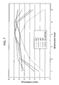
- Fig. 4 is a graph of the measurements of shear strengths at different measurement points after heating resilient adhesives 2, with the thicknesses of thick portions 2a and 2b of the resilient adhesives being different (and the thicknesses of thin portions 2c and 2d of the resilient adhesives being constant).
- the heating temperature is constant at approximately 170°C.
- a first measurement point to a sixth measurement point are disposed in a row in the direction X shown in Fig. 3, with the first measurement point corresponding to an end 10b of the head substrate 10 and the sixth measurement point corresponding to an end 10a of the head substrate 10.
- the shear strength at each measurement point is a ratio with respect to the average shear strengths at the third measurement point and the fourth measurement point.
- the thick portions 2a and 2b of the adhesives 2 have larger thicknesses, the aluminum heat-dissipation plate 1 is allowed to have a wider range of thermal strain.
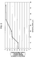
- Fig. 5 is a graph of the measurements of ratios between shear strengths before and after heating the resilient adhesives 2 at the first measurement point or the sixth measurement point, with the thicknesses of the thick portions 2a and 2b of the resilient adhesives 2 being different (and the thicknesses of the thin portions 2c and 2d being constant).
- the heating temperature is constant at, for example, 170°C.
- the thicknesses of the thick portions 2a and 2b are within a range of 10 ⁇ m or less, the ratios between the shear strengths before and after heating are equal to or less than 0.5. Therefore, the adhesive strengths of the thick portions 2a and 2b are approximately halved or more than halved by the heating.
- Fig. 5 is a graph of the measurements of ratios between shear strengths before and after heating the resilient adhesives 2 at the first measurement point or the sixth measurement point, with the thicknesses of the thick portions 2a and 2b of the resilient adhesives 2 being different (and the thicknesses of the thin portions 2c and 2d being constant
- the ratios between the shear strengths before and after the heating also increase. Therefore, when the thicknesses of the thick portions 2a and 2b are in a range exceeding 50 ⁇ m, the ratios between the shear strengths before and after heating are substantially constant at approximately 0.95 or greater. In other words, if the thicknesses of the thick portions 2a and 2b are greater than 50 ⁇ m, a reduction in the adhesive strength by heating can be properly restricted.
- the thicknesses of the thick portions 2a and 2b are at least 50 ⁇ m on the basis of the measurement results shown in Figs. 4 and 5.
- the thicknesses of the thick portions 2a and 2b are substantially equal to an interval d2 between the adhesion surface of the head substrate 10 and the adhesion surfaces defining the wide-gap stepped portions ⁇ 1 and ⁇ 2. Therefore, it is desirable to properly set the adhesion surface interval d2 to a value which can withstand the thermal strain of the aluminum heat-dissipation plate 1.
- the difference between the thicknesses of the thick portions 2a and 2b and those of the thin portions 2c and 2d of the resilient adhesive 2 corresponds to the difference between the height of the upper surface 1a of the aluminum heat-dissipation plate 1 and the surfaces defining the wide-gap stepped portions ⁇ 1 and ⁇ 2.
- the head substrate 10 and the printed circuit board 20 shown in Fig. 1 are provided.
- the aluminum heat-dissipation plate 1 is provided.
- the wide-gap stepped portions ⁇ 1 and ⁇ 2, which increase the interval d between the adhesion surface of the head substrate 10 and that of the aluminum heat-dissipation plate 1, are formed at specific locations of the upper surface 1a of the aluminum heat-dissipation plate 1.
- the first wide-gap stepped portion ⁇ 1 and the second wide-gap stepped portion ⁇ 2 are spaced apart by a predetermined interval in a direction perpendicular to the direction of disposition of the heating resistors 13 at the head substrate 10 to be adhered and secured and are substantially parallel to each other.
- the illustrated X-direction size of the second wide-gap stepped portion ⁇ 2 is larger than that of the first wide-gap stepped portion ⁇ 1.
- the resilient adhesive 2 capable of absorbing thermal strain is applied to the upper surface 1a of the aluminum heat-dissipation plate 1 having the wide-gap stepped portion ⁇ 1 and the wide-gap stepped portion ⁇ 2.
- the resilient adhesive 2 is applied so as to be embedded in the entire wide-gap stepped portion ⁇ 1 and the wide-gap stepped portion ⁇ 2, so that the surface of the resilient adhesive 2 in the wide-gap stepped portion ⁇ 1 and the wide-gap stepped portion ⁇ 2 and the surface of the resilient adhesive 2 on the upper surface 1a of the aluminum heat-dissipation plate 1 are at the same height, thereby forming a flat surface.
- the thick portions 2a and 2b of the resilient adhesive 2 are formed in the wide-gap stepped portion ⁇ 1 and the wide-gap stepped portion ⁇ 2, and the thin portions 2c and 2d of the resilient adhesive 2 are formed on the upper surface 1a of the aluminum heat-dissipation plate 1.
- the thick portions 2a and 2b of the resilient adhesive 2 have thicknesses on the order of 75 ⁇ m, while the thin portions 2c and 2d have thicknesses on the order of 20 ⁇ m.
- the head substrate 10 and the printed circuit board 20 are placed on the aluminum heat-dissipation plate 1 to which the resilient adhesive 2 has been applied.
- the head substrate 10 is disposed so that the end 10a directly below the heating resistors 13 is disposed on the first thick portion 2a, the end 10b directly below the electrode pads 16 is disposed on the second thick portion 2b, and the central portion 10c between the end 10a and the end 10b is disposed on the first thin portion 2c.
- the printed circuit board 20 is disposed so that the end portion 20a where the drive elements 21 are disposed contacts the end 10b of the head substrate 10 and is disposed on the second thick portion 2b and so that an area other than the end portion 20a is disposed on the second thin portion 2d.
- the resilient adhesive 2 is hardened by, for example, heating in order to adhere the aluminum heat-dissipation plate 1 and the head substrate 10 and the printed circuit board 20.
- the adhesion area ⁇ Sa of the head substrate 10 and the first thick portion 2a and the adhesion area ⁇ Sb of the head substrate 10 and the second thick portion 2b are symmetrically disposed with respect to the adhesion area of the head substrate 10 and the first thin portion 2c. Therefore, when the resilient adhesive 2 is hardened, contraction balance is achieved, so that the head substrate 10 is horizontally adhered to the surface of the aluminum heat-dissipation plate 1 without being tilted.
- the individual electrodes 15b at the head substrate 10 and the drive elements 21 at the printed circuit board 20 are electrically connected. More specifically, a surface oxidation layer is broken by applying ultrasonic vibration to the surface of the electrode pad 16 on its corresponding electrode 15b in order to form an Al-Au alloy layer on the electrode pads 16. By this, the electrode pads 16 and the Au joining wire 30 are connected. By the same method, an electrode pad (not shown) disposed on its corresponding drive element 21 and the Au joining wire 30 are connected.
- the aluminum heat-dissipation plate 1 connected to a bonding machine for establishing ground is heated from its back side.
- the aluminum heat-dissipation plate 1, the head substrate 10, and the printed circuit board 20 expand as a result of being heated, their thermal strains are absorbed by the stretching and contraction of the second thick portion 2b of the resilient adhesive 2, so that their original shapes are maintained.
- the electrode pads 16, the separate electrode 15b, and the drive elements 21, etc., connected by the Au joining wire 30 are covered with the sealing resin 31, such as epoxy resin or silicon resin.
- the sealing resin 31 is hardened by, for example, heating for sealing.
- the resilient adhesive 2 prevents the head substrate 10 and the printed circuit board 20 from easily bending. Therefore, even if the sealing resin 31 which has expanded as a result of being heated is hardened, warping of the head substrate 10 and the printed circuit board 20 is properly restricted.
- a surrounding area of the electrode pads 16 and a surrounding area of the drive elements 21 are in a high temperature atmosphere of approximately 120°C or higher by the heating carried out to harden the sealing resin 31 in the sealing step. Excess heat that has been applied is primarily transmitted to the aluminum heat-dissipation plate 1 via the second thin portion 2d of the resilient adhesive 2, and emitted outward from the aluminum heat-dissipation plate 1. The thermal strains of the aluminum heat-dissipation plate 1, the head substrate 10, and the printed circuit board 20 are absorbed by the stretching and contraction of the second thick portion 2b of the resilient adhesive 2.
- the thermal head H1 shown in Fig. 1 is completed.
- the heating resistors 13 When the thermal head H1 is operating, the heating resistors 13 repeatedly generate and dissipate heat in a very short period, and excess heat from the heating resistors 13 is emitted outward via the first thin portion 2c and the first thick portion 2a of the resilient adhesive 2 and the aluminum heat-dissipation plate 1.
- the aluminum heat-dissipation plate 1 tends to expand as a result of being heated, the thermal strains are absorbed by the resiliency of the first thick portion 2a of the resilient adhesive 2.
- the lower surfaces of the printed circuit board 20 and the head substrate 10 are flat surfaces
- the upper surface of the aluminum heat-dissipation plate 1 is a bumpy surface having the wide-gap stepped portions ⁇ 1 and ⁇ 2
- the lower surfaces may be bumpy surfaces and the upper surface may be a flat surface. More specifically, as shown in Fig.
- the surface of an aluminum heat-dissipation plate 1 may be a flat surface 1e which is not bumpy macroscopically, and wide-gap stepped portions ⁇ 3 and ⁇ 4, which increase an interval d between an adhesion surface of a head substrate 10 and an adhesion surface of the aluminum heat-dissipation plate 1 and between an adhesion surface of a printed circuit board 20 and the adhesion surface of the aluminum heat-dissipation plate 1, may be formed in a lower surface 11a of the head substrate 10 and a lower surface 20b of the printed circuit board 20, respectively.
- a resilient adhesive 2 is applied to the lower surfaces of the head substrate 10 and the printed circuit board 20 having the respective wide-gap stepped portions ⁇ 3 and ⁇ 4, and the aluminum heat-dissipation plate 1 is placed thereon.
- the resilient adhesive 2 By hardening the resilient adhesive 2, the aluminum heat-dissipation plate 1 is adhered to the printed circuit board 20 the head substrate 10.
- the positions of the aluminum heat-dissipation plate 1, the head substrate 10, and the printed circuit board 20 do not have to be as strictly determined as in the other embodiment, thereby facilitating production.
- the head substrate 10 used is a rear edge type
- the present invention is applicable to a thermal head using either a partially glazed or a completely glazed head substrate, or to a thermal head using a silicon head substrate.
Landscapes
- Engineering & Computer Science (AREA)
- Manufacturing & Machinery (AREA)
- Electronic Switches (AREA)
- Accessory Devices And Overall Control Thereof (AREA)
Applications Claiming Priority (2)
| Application Number | Priority Date | Filing Date | Title |
|---|---|---|---|
| JP2004100225A JP4476669B2 (ja) | 2004-03-30 | 2004-03-30 | サーマルヘッド及びその製造方法 |
| JP2004100225 | 2004-03-30 |
Publications (3)
| Publication Number | Publication Date |
|---|---|
| EP1582360A2 true EP1582360A2 (de) | 2005-10-05 |
| EP1582360A3 EP1582360A3 (de) | 2006-11-29 |
| EP1582360B1 EP1582360B1 (de) | 2008-11-05 |
Family
ID=34879982
Family Applications (1)
| Application Number | Title | Priority Date | Filing Date |
|---|---|---|---|
| EP05006022A Expired - Lifetime EP1582360B1 (de) | 2004-03-30 | 2005-03-18 | Thermokopf mit zwischen Kühlkörperplatte und Kopfsubstrat aufgetragenem Klebstof und Herstellungsverfahren dafür |
Country Status (5)
| Country | Link |
|---|---|
| US (1) | US7250960B2 (de) |
| EP (1) | EP1582360B1 (de) |
| JP (1) | JP4476669B2 (de) |
| CN (1) | CN100339226C (de) |
| DE (1) | DE602005010774D1 (de) |
Families Citing this family (12)
| Publication number | Priority date | Publication date | Assignee | Title |
|---|---|---|---|---|
| JP3563734B2 (ja) * | 2002-10-29 | 2004-09-08 | ローム株式会社 | サーマルプリントヘッド装置 |
| JP4821290B2 (ja) | 2005-12-01 | 2011-11-24 | パナソニック株式会社 | タッチパネル |
| CN102470677B (zh) * | 2009-08-27 | 2014-10-15 | 京瓷株式会社 | 记录头及具有该记录头的记录装置 |
| US8897046B2 (en) * | 2009-12-25 | 2014-11-25 | Rohm Co., Ltd. | DC voltage conversion module, semiconductor module, and method of making semiconductor module |
| JP2014188980A (ja) * | 2013-03-28 | 2014-10-06 | Toshiba Hokuto Electronics Corp | サーマルプリントヘッド |
| CN107708968B (zh) * | 2015-05-19 | 2020-05-05 | 谷口秀夫 | 造型材料喷出头 |
| CN104859312A (zh) * | 2015-06-08 | 2015-08-26 | 武汉今域通半导体有限公司 | 热敏打印头及其制作方法 |
| JP7031815B2 (ja) * | 2016-10-17 | 2022-03-08 | 東芝ホクト電子株式会社 | サーマルプリントヘッドおよびサーマルプリンタ |
| JP7130990B2 (ja) * | 2018-03-06 | 2022-09-06 | セイコーエプソン株式会社 | 印刷装置 |
| CN110027327B (zh) * | 2019-05-10 | 2020-07-03 | 深圳市博思得科技发展有限公司 | 一种新型宽幅热敏打印头及其制作方法 |
| JP6875616B1 (ja) * | 2019-11-22 | 2021-05-26 | 京セラ株式会社 | サーマルヘッドおよびサーマルプリンタ |
| JPWO2023223806A1 (de) * | 2022-05-17 | 2023-11-23 |
Citations (3)
| Publication number | Priority date | Publication date | Assignee | Title |
|---|---|---|---|---|
| JPH01190467A (ja) | 1988-01-25 | 1989-07-31 | Tdk Corp | サーマルヘッド |
| JPH01131538U (de) | 1988-03-04 | 1989-09-06 | ||
| JPH1128829A (ja) | 1997-07-11 | 1999-02-02 | Mitsubishi Electric Corp | サーマルヘッド |
Family Cites Families (12)
| Publication number | Priority date | Publication date | Assignee | Title |
|---|---|---|---|---|
| JPS60107361A (ja) * | 1983-11-16 | 1985-06-12 | Fuji Xerox Co Ltd | サ−マルヘツド |
| US5285216A (en) * | 1989-09-27 | 1994-02-08 | Kyocera Corporation | Thermal head |
| JPH06238933A (ja) * | 1992-07-03 | 1994-08-30 | Hitachi Koki Co Ltd | サーマルプリントヘッド及びサーマルプリンタ |
| JPH08324014A (ja) * | 1995-05-31 | 1996-12-10 | Kyocera Corp | サーマルヘッド |
| KR0154821B1 (ko) * | 1995-07-14 | 1998-12-01 | 김광호 | 감열 기록 소자 및 그 제조 방법 |
| JPH0966620A (ja) * | 1995-08-30 | 1997-03-11 | Kyocera Corp | サーマルヘッドの製造方法 |
| JP3712513B2 (ja) | 1997-10-24 | 2005-11-02 | 株式会社キッツ | 量水器の支持装置 |
| JP2001301216A (ja) * | 2000-04-24 | 2001-10-30 | Toshiba Corp | サーマルプリントヘッド |
| JP2001315371A (ja) * | 2000-05-11 | 2001-11-13 | Ricoh Elemex Corp | サーマルヘッド |
| JP4493174B2 (ja) * | 2000-07-27 | 2010-06-30 | 京セラ株式会社 | サーマルヘッド |
| JP2002356000A (ja) * | 2001-05-31 | 2002-12-10 | Kyocera Corp | サーマルヘッド |
| JP4360605B2 (ja) * | 2003-04-24 | 2009-11-11 | 京セラ株式会社 | サーマルヘッド及びそれを用いたサーマルプリンタ |
-
2004
- 2004-03-30 JP JP2004100225A patent/JP4476669B2/ja not_active Expired - Fee Related
-
2005
- 2005-03-18 DE DE602005010774T patent/DE602005010774D1/de not_active Expired - Fee Related
- 2005-03-18 EP EP05006022A patent/EP1582360B1/de not_active Expired - Lifetime
- 2005-03-29 US US11/092,181 patent/US7250960B2/en not_active Expired - Fee Related
- 2005-03-30 CN CNB2005100639124A patent/CN100339226C/zh not_active Expired - Fee Related
Patent Citations (3)
| Publication number | Priority date | Publication date | Assignee | Title |
|---|---|---|---|---|
| JPH01190467A (ja) | 1988-01-25 | 1989-07-31 | Tdk Corp | サーマルヘッド |
| JPH01131538U (de) | 1988-03-04 | 1989-09-06 | ||
| JPH1128829A (ja) | 1997-07-11 | 1999-02-02 | Mitsubishi Electric Corp | サーマルヘッド |
Also Published As
| Publication number | Publication date |
|---|---|
| JP4476669B2 (ja) | 2010-06-09 |
| CN100339226C (zh) | 2007-09-26 |
| JP2005280203A (ja) | 2005-10-13 |
| EP1582360A3 (de) | 2006-11-29 |
| US7250960B2 (en) | 2007-07-31 |
| CN1676342A (zh) | 2005-10-05 |
| DE602005010774D1 (de) | 2008-12-18 |
| EP1582360B1 (de) | 2008-11-05 |
| US20050219349A1 (en) | 2005-10-06 |
Similar Documents
| Publication | Publication Date | Title |
|---|---|---|
| JP3627738B2 (ja) | 半導体装置 | |
| EP1582360B1 (de) | Thermokopf mit zwischen Kühlkörperplatte und Kopfsubstrat aufgetragenem Klebstof und Herstellungsverfahren dafür | |
| JP2001326236A (ja) | 半導体装置の製造方法 | |
| US20210280534A1 (en) | Semiconductor device and method for manufacturing semiconductor device | |
| JP2009226868A (ja) | サーマルプリントヘッド | |
| CN100352662C (zh) | 热敏头及其制造方法 | |
| JP2828358B2 (ja) | 半導体放熱構造 | |
| JP2000331138A (ja) | 非接触型icカード | |
| JP3905311B2 (ja) | サーマルヘッドユニット、サーマルヘッドの製造方法、及びサーマルヘッドユニットの製造方法 | |
| US20050250245A1 (en) | Semiconductor chip arrangement and method | |
| JPS6048375A (ja) | サ−マルヘツドおよびその製造方法 | |
| CN212353294U (zh) | 一种能够抑制基板弯曲的热敏打印头 | |
| JPH09180973A (ja) | 半導体装置およびその製造方法 | |
| JP4068647B2 (ja) | サーマルヘッドの製造方法 | |
| JP2002036615A (ja) | サーマルヘッド | |
| JPH08113765A (ja) | 熱接着複合テープ | |
| JPH02102565A (ja) | 半導体装置 | |
| JPH0724330B2 (ja) | 混成集積回路装置 | |
| JPH07283265A (ja) | ボンディング用加熱装置 | |
| CN117400638A (zh) | 拼接热敏打印头及其制造方法 | |
| JPH0499653A (ja) | サーマルヘッド | |
| JP2000043305A (ja) | サーマルヘッドおよびその製造方法 | |
| JPH0867022A (ja) | サーマルプリントヘッド及びその基板の製造方法 | |
| JP3066845B2 (ja) | サーマルヘッドの製造方法 | |
| JPH11204312A (ja) | 複合電子部品およびその製造方法 |
Legal Events
| Date | Code | Title | Description |
|---|---|---|---|
| PUAI | Public reference made under article 153(3) epc to a published international application that has entered the european phase |
Free format text: ORIGINAL CODE: 0009012 |
|
| AK | Designated contracting states |
Kind code of ref document: A2 Designated state(s): AT BE BG CH CY CZ DE DK EE ES FI FR GB GR HU IE IS IT LI LT LU MC NL PL PT RO SE SI SK TR |
|
| AX | Request for extension of the european patent |
Extension state: AL BA HR LV MK YU |
|
| PUAL | Search report despatched |
Free format text: ORIGINAL CODE: 0009013 |
|
| AK | Designated contracting states |
Kind code of ref document: A3 Designated state(s): AT BE BG CH CY CZ DE DK EE ES FI FR GB GR HU IE IS IT LI LT LU MC NL PL PT RO SE SI SK TR |
|
| AX | Request for extension of the european patent |
Extension state: AL BA HR LV MK YU |
|
| 17P | Request for examination filed |
Effective date: 20061208 |
|
| 17Q | First examination report despatched |
Effective date: 20070129 |
|
| AKX | Designation fees paid |
Designated state(s): DE FR GB |
|
| GRAP | Despatch of communication of intention to grant a patent |
Free format text: ORIGINAL CODE: EPIDOSNIGR1 |
|
| GRAS | Grant fee paid |
Free format text: ORIGINAL CODE: EPIDOSNIGR3 |
|
| GRAA | (expected) grant |
Free format text: ORIGINAL CODE: 0009210 |
|
| AK | Designated contracting states |
Kind code of ref document: B1 Designated state(s): DE FR GB |
|
| REG | Reference to a national code |
Ref country code: GB Ref legal event code: FG4D |
|
| REF | Corresponds to: |
Ref document number: 602005010774 Country of ref document: DE Date of ref document: 20081218 Kind code of ref document: P |
|
| PGFP | Annual fee paid to national office [announced via postgrant information from national office to epo] |
Ref country code: GB Payment date: 20090107 Year of fee payment: 5 |
|
| PGFP | Annual fee paid to national office [announced via postgrant information from national office to epo] |
Ref country code: DE Payment date: 20090528 Year of fee payment: 5 |
|
| PLBE | No opposition filed within time limit |
Free format text: ORIGINAL CODE: 0009261 |
|
| STAA | Information on the status of an ep patent application or granted ep patent |
Free format text: STATUS: NO OPPOSITION FILED WITHIN TIME LIMIT |
|
| 26N | No opposition filed |
Effective date: 20090806 |
|
| PGFP | Annual fee paid to national office [announced via postgrant information from national office to epo] |
Ref country code: FR Payment date: 20081217 Year of fee payment: 5 |
|
| GBPC | Gb: european patent ceased through non-payment of renewal fee |
Effective date: 20100318 |
|
| REG | Reference to a national code |
Ref country code: FR Ref legal event code: ST Effective date: 20101130 |
|
| PG25 | Lapsed in a contracting state [announced via postgrant information from national office to epo] |
Ref country code: FR Free format text: LAPSE BECAUSE OF NON-PAYMENT OF DUE FEES Effective date: 20100331 |
|
| PG25 | Lapsed in a contracting state [announced via postgrant information from national office to epo] |
Ref country code: DE Free format text: LAPSE BECAUSE OF NON-PAYMENT OF DUE FEES Effective date: 20101001 |
|
| PG25 | Lapsed in a contracting state [announced via postgrant information from national office to epo] |
Ref country code: GB Free format text: LAPSE BECAUSE OF NON-PAYMENT OF DUE FEES Effective date: 20100318 |