EP1580718B1 - Display and its driving method, and electronic device - Google Patents
Display and its driving method, and electronic device Download PDFInfo
- Publication number
- EP1580718B1 EP1580718B1 EP03772788A EP03772788A EP1580718B1 EP 1580718 B1 EP1580718 B1 EP 1580718B1 EP 03772788 A EP03772788 A EP 03772788A EP 03772788 A EP03772788 A EP 03772788A EP 1580718 B1 EP1580718 B1 EP 1580718B1
- Authority
- EP
- European Patent Office
- Prior art keywords
- electrode
- electrically connected
- erasure
- driving
- emitting element
- Prior art date
- Legal status (The legal status is an assumption and is not a legal conclusion. Google has not performed a legal analysis and makes no representation as to the accuracy of the status listed.)
- Expired - Fee Related
Links
Images


Classifications
-
- G—PHYSICS
- G09—EDUCATION; CRYPTOGRAPHY; DISPLAY; ADVERTISING; SEALS
- G09G—ARRANGEMENTS OR CIRCUITS FOR CONTROL OF INDICATING DEVICES USING STATIC MEANS TO PRESENT VARIABLE INFORMATION
- G09G3/00—Control arrangements or circuits, of interest only in connection with visual indicators other than cathode-ray tubes
- G09G3/20—Control arrangements or circuits, of interest only in connection with visual indicators other than cathode-ray tubes for presentation of an assembly of a number of characters, e.g. a page, by composing the assembly by combination of individual elements arranged in a matrix no fixed position being assigned to or needed to be assigned to the individual characters or partial characters
- G09G3/22—Control arrangements or circuits, of interest only in connection with visual indicators other than cathode-ray tubes for presentation of an assembly of a number of characters, e.g. a page, by composing the assembly by combination of individual elements arranged in a matrix no fixed position being assigned to or needed to be assigned to the individual characters or partial characters using controlled light sources
- G09G3/30—Control arrangements or circuits, of interest only in connection with visual indicators other than cathode-ray tubes for presentation of an assembly of a number of characters, e.g. a page, by composing the assembly by combination of individual elements arranged in a matrix no fixed position being assigned to or needed to be assigned to the individual characters or partial characters using controlled light sources using electroluminescent panels
-
- G—PHYSICS
- G09—EDUCATION; CRYPTOGRAPHY; DISPLAY; ADVERTISING; SEALS
- G09G—ARRANGEMENTS OR CIRCUITS FOR CONTROL OF INDICATING DEVICES USING STATIC MEANS TO PRESENT VARIABLE INFORMATION
- G09G3/00—Control arrangements or circuits, of interest only in connection with visual indicators other than cathode-ray tubes
- G09G3/20—Control arrangements or circuits, of interest only in connection with visual indicators other than cathode-ray tubes for presentation of an assembly of a number of characters, e.g. a page, by composing the assembly by combination of individual elements arranged in a matrix no fixed position being assigned to or needed to be assigned to the individual characters or partial characters
-
- G—PHYSICS
- G09—EDUCATION; CRYPTOGRAPHY; DISPLAY; ADVERTISING; SEALS
- G09G—ARRANGEMENTS OR CIRCUITS FOR CONTROL OF INDICATING DEVICES USING STATIC MEANS TO PRESENT VARIABLE INFORMATION
- G09G2300/00—Aspects of the constitution of display devices
- G09G2300/04—Structural and physical details of display devices
- G09G2300/0439—Pixel structures
- G09G2300/0452—Details of colour pixel setup, e.g. pixel composed of a red, a blue and two green components
-
- G—PHYSICS
- G09—EDUCATION; CRYPTOGRAPHY; DISPLAY; ADVERTISING; SEALS
- G09G—ARRANGEMENTS OR CIRCUITS FOR CONTROL OF INDICATING DEVICES USING STATIC MEANS TO PRESENT VARIABLE INFORMATION
- G09G2300/00—Aspects of the constitution of display devices
- G09G2300/08—Active matrix structure, i.e. with use of active elements, inclusive of non-linear two terminal elements, in the pixels together with light emitting or modulating elements
- G09G2300/0809—Several active elements per pixel in active matrix panels
- G09G2300/0814—Several active elements per pixel in active matrix panels used for selection purposes, e.g. logical AND for partial update
-
- G—PHYSICS
- G09—EDUCATION; CRYPTOGRAPHY; DISPLAY; ADVERTISING; SEALS
- G09G—ARRANGEMENTS OR CIRCUITS FOR CONTROL OF INDICATING DEVICES USING STATIC MEANS TO PRESENT VARIABLE INFORMATION
- G09G2300/00—Aspects of the constitution of display devices
- G09G2300/08—Active matrix structure, i.e. with use of active elements, inclusive of non-linear two terminal elements, in the pixels together with light emitting or modulating elements
- G09G2300/0809—Several active elements per pixel in active matrix panels
- G09G2300/0842—Several active elements per pixel in active matrix panels forming a memory circuit, e.g. a dynamic memory with one capacitor
-
- G—PHYSICS
- G09—EDUCATION; CRYPTOGRAPHY; DISPLAY; ADVERTISING; SEALS
- G09G—ARRANGEMENTS OR CIRCUITS FOR CONTROL OF INDICATING DEVICES USING STATIC MEANS TO PRESENT VARIABLE INFORMATION
- G09G2310/00—Command of the display device
- G09G2310/02—Addressing, scanning or driving the display screen or processing steps related thereto
- G09G2310/0235—Field-sequential colour display
-
- G—PHYSICS
- G09—EDUCATION; CRYPTOGRAPHY; DISPLAY; ADVERTISING; SEALS
- G09G—ARRANGEMENTS OR CIRCUITS FOR CONTROL OF INDICATING DEVICES USING STATIC MEANS TO PRESENT VARIABLE INFORMATION
- G09G2310/00—Command of the display device
- G09G2310/02—Addressing, scanning or driving the display screen or processing steps related thereto
- G09G2310/0264—Details of driving circuits
- G09G2310/0267—Details of drivers for scan electrodes, other than drivers for liquid crystal, plasma or OLED displays
-
- G—PHYSICS
- G09—EDUCATION; CRYPTOGRAPHY; DISPLAY; ADVERTISING; SEALS
- G09G—ARRANGEMENTS OR CIRCUITS FOR CONTROL OF INDICATING DEVICES USING STATIC MEANS TO PRESENT VARIABLE INFORMATION
- G09G2310/00—Command of the display device
- G09G2310/02—Addressing, scanning or driving the display screen or processing steps related thereto
- G09G2310/0264—Details of driving circuits
- G09G2310/027—Details of drivers for data electrodes, the drivers handling digital grey scale data, e.g. use of D/A converters
-
- G—PHYSICS
- G09—EDUCATION; CRYPTOGRAPHY; DISPLAY; ADVERTISING; SEALS
- G09G—ARRANGEMENTS OR CIRCUITS FOR CONTROL OF INDICATING DEVICES USING STATIC MEANS TO PRESENT VARIABLE INFORMATION
- G09G3/00—Control arrangements or circuits, of interest only in connection with visual indicators other than cathode-ray tubes
- G09G3/20—Control arrangements or circuits, of interest only in connection with visual indicators other than cathode-ray tubes for presentation of an assembly of a number of characters, e.g. a page, by composing the assembly by combination of individual elements arranged in a matrix no fixed position being assigned to or needed to be assigned to the individual characters or partial characters
- G09G3/2007—Display of intermediate tones
- G09G3/2018—Display of intermediate tones by time modulation using two or more time intervals
- G09G3/2022—Display of intermediate tones by time modulation using two or more time intervals using sub-frames
-
- G—PHYSICS
- G09—EDUCATION; CRYPTOGRAPHY; DISPLAY; ADVERTISING; SEALS
- G09G—ARRANGEMENTS OR CIRCUITS FOR CONTROL OF INDICATING DEVICES USING STATIC MEANS TO PRESENT VARIABLE INFORMATION
- G09G3/00—Control arrangements or circuits, of interest only in connection with visual indicators other than cathode-ray tubes
- G09G3/20—Control arrangements or circuits, of interest only in connection with visual indicators other than cathode-ray tubes for presentation of an assembly of a number of characters, e.g. a page, by composing the assembly by combination of individual elements arranged in a matrix no fixed position being assigned to or needed to be assigned to the individual characters or partial characters
- G09G3/22—Control arrangements or circuits, of interest only in connection with visual indicators other than cathode-ray tubes for presentation of an assembly of a number of characters, e.g. a page, by composing the assembly by combination of individual elements arranged in a matrix no fixed position being assigned to or needed to be assigned to the individual characters or partial characters using controlled light sources
- G09G3/30—Control arrangements or circuits, of interest only in connection with visual indicators other than cathode-ray tubes for presentation of an assembly of a number of characters, e.g. a page, by composing the assembly by combination of individual elements arranged in a matrix no fixed position being assigned to or needed to be assigned to the individual characters or partial characters using controlled light sources using electroluminescent panels
- G09G3/32—Control arrangements or circuits, of interest only in connection with visual indicators other than cathode-ray tubes for presentation of an assembly of a number of characters, e.g. a page, by composing the assembly by combination of individual elements arranged in a matrix no fixed position being assigned to or needed to be assigned to the individual characters or partial characters using controlled light sources using electroluminescent panels semiconductive, e.g. using light-emitting diodes [LED]
Definitions
- the present invention relates to a display device disposed with light-emitting elements, particularly a display device disposed with a display portion that conducts multicolor display, and to a driving method thereof.
- Fig. 5(A) shows an example of a common color display device.
- a pixel portion 501, a source signal line drive circuit 502 and a gate signal line drive circuit 503 are formed on a substrate 500.
- the input of signals to the drive circuits and the supply of an electrical current to the pixel portion 501 are conducted from the outside via a flexible printed circuit (FPC) 504.
- FPC flexible printed circuit
- Fig. 5(A) the portion represented by the dotted line frame 510 is one pixel.
- Fig. 5(B) shows an enlarged view of part of the pixel portion 501.
- Each pixel respectively includes a source signal line 511 for inputting an image signal, a gate signal line 512 for conducting line selection, a current supply line 513 for supplying an electrical current to an EL element 516, a transistor 514 for switching, a transistor 515 for driving, a power line 517 and a retention volume 518.
- Patent Document 1 there is description in Patent Document 1 in relation to a circuit configuration where one pixel is configured using two transistors and which drives a load (here, the EL element is used as an example).
- the respective emissions of R, G and B are controlled using, for example, three adjacent pixels represented by the dotted frame 520 in Fig. 5(A) , and multicolor display is conducted by mixing these colors. In other words, three pixels are required for a 1-bit display.
- the pixels of a color display device with which multicolor display is possible have many constituent elements, and the area occupying the display region is also large. Thus, the aperture ratio drops.
- it is necessary to raise the current density per pixel but this leads to a reduction in the life of the EL elements.
- EP 1204087 A1 discloses a full color LED display system for displaying gradation rich multicolor images by combining LED lamps of three primary colors of RGB (red, green, blue).
- this disclosure describes a system wherein a pulse-width modulation method is applied for lighting and activating an LED lamp by an activating pulse having been pulsed-width modulated based on gradation data for each color.
- US 6,429,601 B1 discloses an electroluminescent device having an organic light-emitting region comprising a plurality of organic light emitting pixels; which means each associated with a respective pixel for switching power to that pixel; and drive means for driving each switch means to cycle between a first, low power mode and a second, high power mode, at the frequency sufficient to cause light emission from the associated pixel to appeal substantially continuous, the duration of the high power mode relative to the low power mode being variable so as to vary the average brightness of the pixel.
- the present invention has been made in light of the above problem and provides a display device with which multicolor display is possible using a new configuration.
- one pixel has conventionally been configured as three RGB sub-pixels
- EL elements that emit respective emission colors of R, G and B are laminated and formed.
- the source signal line and the gate signal line are not disposed for R, G and B; rather, one signal line is shared by three pixels.
- the emissions of R, G and B are conducted in respective different periods.
- the field sequential format where R, G and B are sequentially emitted in one frame period, is used.
- RGB are selected by selecting the potential of the current supply lines so that a desired emission color can be obtained.
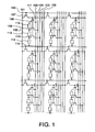
- FIG 1 shows the configuration of a pixel portion in a display device of the present invention.
- a thin film transistor referred to below as a "TFT"
- the present invention is not limited thereto and includes all cases where the transistor is configured by using an organic thin film transistor, a MOS transistor, a molecular transistor or the like.
- a first electrode and the other will be referred to as a second electrode.
- the present invention will be described using EL elements as an example of light-emitting elements, the present invention is not limited thereto and includes, as targets, elements with which an electrical current can be generated by imparting a potential difference between the two terminals so that the elements can emit light due to the electrical current.
- each pixel respectively includes a source signal line 101, a gate signal line 102, first to third current supply lines 103 to 105, a retention volume line 106, a TFT for switching 107, first to third TFTs for driving 108 to 110, a retention volume 111, first to third EL elements 112 to 114, and a power supply line 115.
- the gate electrode of the TFT for switching 107 is electrically connected to the gate signal line 102, the first electrode is electrically connected to the source signal line 101, and the second electrode is electrically connected to the gate electrodes of the first to third TFTs for driving 108 to 110.
- the first electrode of the first TFT for driving 108 is electrically connected to the first current supply line 103, and the second electrode is electrically connected to the first electrode of the first EL element 112.
- the first electrode of the second TFT for driving 109 is electrically connected to the second current supply line 104, and the second electrode is electrically connected to the first electrode of the second EL element 113.
- the first electrode of the third TFT for driving 110 is electrically connected to the third current supply line 105, and the second electrode is electrically connected to the first electrode of the third EL element 114.
- the retention volume 111 is formed between the retention volume line 106 and the gate electrodes of the first to third TFTs for driving 108 to 110, and retains the potentials of the gate electrodes of the first to third TFTs for driving 108 to 110.
- the retention volume 111 is formed using the independent retention volume line 106, but the present invention is not particularly limited to this configuration. In other words, the retention volume 111 may be disposed between the gate electrodes of the first to third TFTs for driving 108 to 110 and any constant potential.
- the first to third EL elements 112 to 114 are formed by lamination.
- the second electrode of the first EL element 112 doubles as the first electrode of the second EL element 113
- the second electrode of the second EL element 113 doubles as the first electrode of the third EL element 114.
- the second electrode of the third EL element 114 is electrically connected to the power supply line 115 and has a different potential from those of the first to third power supply lines 103 to 105.
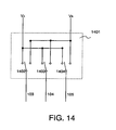
- the first to third current supply lines 103 to 105 are connected to a control circuit 1401 of Fig. 14 .
- the control circuit 1401 switches the connections of switches 1402 to 1404 respectively, whereby it controls the potentials of the current supply lines 103 to 105 to be V A or V C . Thus, it conducts field sequential driving.
- the configuration of the control circuit is not limited to Fig. 14 . In Fig. 14 , the control circuit has a configuration using the two potentials of V A and V C , but the control circuit may also have a configuration that switches three or more potentials.
- the first electrodes of the second and third EL elements 113 and 114 are both formed by using a transparent conductive material. Also, one of the first electrode of the first EL element 112 and the second electrode of the third EL element 114 is formed by using a transparent conductive material. The emission light from the first to third EL elements 112 to 114 appears outside through the electrode formed by the transparent conductive material which of the first electrode of the first EL element 112 and the second electrode of the third EL element 114.
- ON and OFF refer to the state of the TFT.
- ON is meant a state where the absolute value of the voltage between the gate and the source of the TFT exceeds the absolute value of the threshold thereof, so that an electrical current flows between the source and the drain.
- OFF is meant a state where the absolute value of the voltage between the gate and the source of the TFT is less than the absolute value of the threshold thereof, so that an electrical current does not flow between the source and the drain (does not include a minute leak current).
- the TFT for switching 107 When the gate signal line 102 is selected, the TFT for switching 107 is turned ON and, as shown in FIG 9(A) , an image signal is inputted from the source signal line 101 to the gate electrodes of the first to third TFTs for driving 108 to 110 via the TFT for switching 107.
- the TFT for switching 107 uses an N-type TFT and the first to third TFTs for driving 108 to 110 use P-type TFTs.
- the potential of the image signal is an L potential
- the first to third TFTs for driving 108 to 110 are turned ON.
- the EL elements are laminated.
- control of the light emission/non-light emission of the EL elements is conducted by controlling the potentials of the first to third current supply lines 103 to 105.
- the potential of the power line is an opposing voltage V C
- the potentials of the first to third current supply lines 103 to 105 are V A , V C and V C (where V C ⁇ V A ).
- the potential of the first electrode generally becomes V A and the potential of the second electrode generally becomes V C .
- the potential of the first electrode of the second EL element 113 is generally V C because it is the potential of the second electrode of the first EL element 112, and the potential of the second electrode is also generally V C .
- an electrical current does not flow to the second EL element 113. Namely, the second EL element 113 does not emit light at this time.
- the electrical current flowing to the first EL element 112 from the first current supply line 103 flows to the second current supply line 104 via the second TFT 109 for driving.
- an electrical current does not flow thereto because there is no difference in potential between the first electrode and the second electrode. Namely, it does not emit light.
- the potential of the power line is an opposing voltage V C
- the potentials of the first to third current supply lines 103 to 105 are V A , V A and V C .
- the potential of the first electrode generally becomes V A and the potential of the second electrode also generally becomes V A .
- an electrical current does not flow to the first EL element 112. Namely, it does not emit light.
- the potential of the first electrode is generally V A because it is the potential of the second electrode of the first EL element 112, and the potential of the second electrode is generally V C .
- a difference in potential arises between the first electrode and the second electrode, electrical current flows thereto via the second TFT for driving 109, and the second EL element 113 emits light.
- the potential of the first electrode is generally V C and the potential of the second electrode is also V C .
- an electrical current does not flow thereto because there is no difference in potential between the first electrode and the second electrode. Namely, it does not emit light.
- the potential of the power line is an opposing voltage V C
- the potentials of the first to third current supply lines 103 to 105 are all V A .
- the potential of the first electrode generally becomes V A and the potential of the second electrode also generally becomes V A .
- an electrical current does not flow to the first EL element 112. Namely, it does not emit light.
- the electrical current does not flow thereto because there is no difference in potential between the first electrode and the second electrode. Namely, it does not emit light.
- the potential of the first electrode generally becomes V A and the potential of the second electrode is V C .
- a difference in potential arises between the first electrode and the second electrode, electrical current flows thereto via the third TFT for driving 110, and the third EL element 114 emits light.
- the EL elements formed by lamination can be made to selectively emit light.
- the difference in potential between the first electrodes and the second electrodes of the first to third EL elements 112 to 114 i.e. the voltage between the anode/cathode is V A -V C , but because it is common in the case of EL elements for the voltage between the anode and cathode necessary to obtain an identical luminance to be different due to the emission colors, the present invention is not limited to the above-described conditions. In other words, an appropriate voltage may be set depending on the characteristics of the EL elements.
- the gist of the present invention lies in causing any one light-emitting element to selectively emit light for a certain period of time in a case that includes a plurality of light-emitting elements, so that realization of the present invention is easily possible with a similar technique even in the case of, for example, three or more colors.
- the number of light-emitting elements is not particularly limited.
- the first to third light-emitting elements have a laminate structure
- the present invention can be applied even if the respective light-emitting elements are not necessarily laminated.
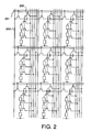
- FIG 2 shows an example where the present invention is applied to pixels of a configuration that is different from those of embodiment mode 1.
- a gate signal line for erasure 201 and a TFT for erasure 202 are added to the configuration shown in FIG. 1 . Because the remaining configuration is in accordance with FIG 1 , numbers will be omitted.
- the EL elements emitting light can be forcibly placed in a non-light-emitting state at a desired timing in order to control the emission time when conducting display according to the digital time gradation described in Japanese Patent Laid-open No. 2001-343933 .
- a line selection pulse is outputted to the gate signal line for erasure 201 at the timing at which one desires to end light emission, whereby the TFT for erasure 202 is turned ON.
- the potentials of the gate electrodes of the TFTs for driving 108 to 110 become equal to the potential of the retention volume line and the TFTs for driving 108 to 110 are turned OFF.
- the paths by which the electrical currents are supplied to the EL elements are cut off and the EL elements are placed in a non-light-emitting state.
- the potential of the retention volume line 106 is a potential at which the TFTs for driving 108 to 110 are reliably turned OFF.
- the potential of the retention volume line 106 is made higher than the potentials of all the current supply lines.
- the potential of the retention volume line 106 is configured so that the voltages between the gates/sources of the TFTs for driving 108 to 110 all become positive.
- the potential of the retention volume line 106 may be made less than the potentials of all the current supply lines.
- the TFT for erasure 202 is disposed between the gate electrodes of the TFTs for driving 108 to 110 and the retention volume line 106, but it may also be disposed between the gate electrodes of the TFTs for driving 108 to 110 and any of the first to third current supply lines 103 to 105.
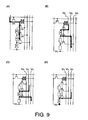
- the TFT for erasure 202 is not limited to the disposition in Fig. 2 . It suffices as long as the TFT for erasure can be controlled at a desired timing so that the supply of the electrical current to the EL elements can be blocked. For example, as shown in Fig.
- TFTs for erasure 1002 to 1004 can be disposed between the drain terminals of the TFTs for driving 108 to 110 and the EL elements, and with respect to the period in which the TFTs for erasure 1002 to 1004 are ON, the electrical current flows to the EL elements via any of the TFTs for driving 108 to 110, and the TFTs for erasure 1002 to 1004 are turned OFF at a desired timing, whereby the electrical current to the EL elements can be forcibly blocked.
- FIG 6 shows a configuration example of a source signal line drive circuit for conducting display using analog image signals as mainly image signals.
- the source signal line drive circuit includes a shift register 602 using a plurality of flip-flops 601, NANDs 603, level shifters 604, buffers 605 and sampling switches 606.
- the shift register 602 sequentially outputs sampling pulses in accordance with clock signals (S-CK, S-CKb) and a start pulse (S-SP). Sometimes two continuous sampling pulses have a period in which their mutual pulses overlap. In such a case, computation is conducted with the before and after sampling pulses by the NANDs 603. Depending on the configuration of the shift register 602, sometimes the NANDs 603 are not necessary.
- sampling pulses outputted from the NANDs 603 undergo amplitude conversion by the level shifters 604, are amplified by the buffers 605 and are inputted to the sampling switches 606.
- the sampling switches 606 fetch analog image signals (Video) being inputted at the timing at which the sampling pulses are inputted and point-sequentially output them to source signal lines S 1 to S n .
- the level shifters 604 and the buffers 605 are not particularly necessary as long as the function of the shift register 602 itself or the NANDs 603 themselves driving a large load is sufficient.
- FIG 6(B) The basic configuration of FIG 6(B) is the same as that of Fig. 6(A) , except that the buffers 605 drive a plurality of sampling switches 606 per column.
- fetching of the image signals can be simultaneously conducted in a plurality of rows at the timing at which one sampling pulse is outputted, so that, in comparison to the configuration of FIG 6(A) , the operating frequency of the source signal line drive circuit can be lowered.
- driving so that fetching of the image signals is conducted by one sampling pulse simultaneously for k number of image signals is called k divisional driving, and as long as the number of source signal lines is the same, this suffices at an operating frequency of 1/k with respect to the configuration shown in FIG 6(A) .
- k divisional driving driving so that fetching of the image signals is conducted by one sampling pulse simultaneously for k number of image signals
- input of k number of image signals in parallel becomes necessary.
- FIG. 7 shows a configuration example of a source signal line drive circuit for conducting display using digital image signals as mainly image signal.
- the source signal line drive circuit includes a shift register 702 using a plurality of flip-flops 701, NANDs 703, first latch circuits 704, second latch circuits 705 and D/A conversion circuits 706.
- Fetching of the digital image signals (Data) is conducted in the first latch circuits 704 in accordance with the timing at which the sampling pulses are inputted.
- fetching of 3-bit digital image signals is simultaneously conducted by three parallel first latch circuits 704.
- the fetched digital image signals are retained in the respective first latch circuits 704.
- the above-described operation is conducted in order beginning with the first row.
- latch signals (LAT) are inputted after fetching of the digital image signals in the final row of first latch circuits 704 ends, the digital image signals being retained in the first latch circuits 704 are sent concurrently to the second latch circuits 705. Thereafter, the digital image signals of one line are processed in parallel.
- the digital image signals sent to the second latch circuits 705 are next inputted to the D/A conversion circuits 706, undergo D/A conversion, are converted to analog voltage signals and outputted to the source signal lines S 1 to S n .
- FIG 7(B) a configuration in the case of conducting display by digital time gradation is shown.
- the first latch circuits 704 and the second latch circuits 705 are singly disposed per one row, and the digital image signals (Data) are serially inputted from one signal line. As an example, they are inputted in the following manner: first bit data of the first row ⁇ first bit data of second row ⁇ ⁇ ⁇ first bit data of final row ⁇ second bit data of first row ⁇ second bit data of second row ⁇ ⁇ ⁇ second bit data of final row ⁇ ⁇ last bit data of first row ⁇ last bit data of second row ⁇ ⁇ ⁇ last bit data of final row; but the manner of input is not limited to this. Because the operation of each part is the same as in FIG 7(A) , description thereof will be omitted here.
- FIG 8 shows a configuration example of a gate signal line drive circuit.
- the gate signal line drive circuit includes, similar to the source signal line drive circuit, a shift register 802 using a plurality of flip-flips 801, NANDs 803, level shifters 804 and buffers 805.
- the NANDs 802, the level shifters 803 and the buffers 804 may be disposed as necessary.
- line selection pulses are sequentially outputted from the shift register 802, computation between adjacent pulses is conducted in the NANDs 803, the pulses undergo amplitude conversion in the level shifters 804, are outputted to gate signal lines G 1 to G m via the buffers 805 and selected in order beginning with the first line.
- the gate signal line drive circuit may also be used in combination with any of the above-described source signal line drive circuits.
- rewriting of the screen and display are repeatedly conducted in a display period in the display device.
- the number of times of rewriting is usually about 60 per second, so that the viewer does not perceive flickering.
- the period in which the series of operations of rewriting and display of the screen are conducted one time i.e. the period represented by 301 in FIG 3(A) will be described as one frame period.
- image signals to the pixels emitting the first to third emission colors are inputted from a common source signal line.
- the field sequential format is used.
- one frame period is divided into three periods, and writing and light emission are conducted per emission color in the respective periods.
- the colors are perceived as being mixed due to the afterimage effect, so that multicolor display becomes possible.
- the periods represented by Ta1 to Ta3 are periods in which the image signals are written to the pixels, and will hereafter be referred to as address (writing) periods.
- the periods represented by Ts1 to Ts3 are periods in which light is emitted at a desired luminance in response to the written image signals, and will hereafter be referred to as sustain (light emission) periods.
- line selection is conducted from line 1 sequentially to line m (final line).
- the period represented by 302 i.e. the selection period per one line will be referred to as one horizontal period. Writing of dot data of n rows is conducted within one horizontal period.
- FIG 3(D) is an example of a case where writing of dot data within one horizontal period is conducted in a line sequence.
- sampling of dot data from the first row sequentially to the nth row is conducted in the first latch circuits in the period represented by 303, and when sampling of the data of one line ends, latch pulses are inputted at the timing represented by 305 during the flyback period represented by 304, and at this time the data of one line are sent altogether to the second latch circuits.
- FIG 3(E) is an example of a case where writing of dot data within one horizontal period is conducted in a point sequence. As described in comparative example 1 sampling of dot data from the first row sequentially to the nth row is conducted in the period represented by 306, and in each row the data is immediately outputted to the source signal line.
- the field sequential format is also used in digital time gradation.
- One frame period represented by 401 in FIG. 4(A) is divided into three periods represented by 402 to 404, and writing and display in each emission color are conducted in each period.
- the frame period 302 is further divided into a plurality of sub-frame periods.
- the data are 3-bit, they are divided into the three subframe periods.
- Each subframe period includes an address (writing) period Ta# (# is a natural number) and a sustain (light emission) period Ts#.
- the address (writing) periods and the sustain (light emission) periods are completely separate, there is the advantage that the lengths of the sustain (light emission) periods can be freely set, but as writing is being conducted in a certain line in an address (writing) period, writing and light emission are not conducted in other lines. In other words, the duty ratio drops overall.
- the operation here is the same in that one frame period represented by 411 in FIG. 4(B) is divided into three frame periods represented by 412 to 414, but is different in that the address (writing) periods and the sustain (light emission) periods are not divided in each sub-frame period.
- the address (writing) periods and the sustain (light emission) periods are not divided in each sub-frame period.
- erasure periods Tr1 3 , Tr2 3 and Tr3 3 are forcibly disposed using the TFT for erasure from the point in time when the sustain (light emission) period ends to when the next address (writing) period begins. Due to these erasure periods, address (writing) periods in different sub-frame periods can be prevented from overlapping.
- selection pulses for erasure are outputted using the second gate signal line drive circuit for controlling the TFTs for erasure so that the TFTs for erasure are turned ON at a desired timing in order beginning with the first line.
- the second gate signal line drive circuit may have the same configuration as the first gate signal line drive circuit that conducts ordinary writing.
- the lengths of periods Te1 3 , Te2 3 and Te3 3 that conduct writing of erasure signals (hereinafter referred to as reset periods) are equal to those of the address (writing) periods.
- a case where the number of gradation display bits was the same as the number of sub-frames was used as an example, but they may be divided into more periods. It is also possible to realize gradation even if the ratio of the lengths of the sustain (light emission) periods is not the power of two.
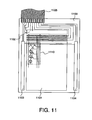
- FIG 11 the configuration of a display device for driving pixels including a TFT for erasure such as shown in FIG 2 and FIG. 10 will be described.
- a pixel portion 1101, a source signal line drive circuit 1102, a first gate signal line drive circuit 1103 and a second gate signal line drive circuit 1104 are formed on a substrate 1100. Input of signals to the drive circuits and supply of an electrical current to the pixel portion 1101 are conducted from the outside via a flexible printed circuit (FPC) 1105.
- the portion represented by the dotted frame 1110 is one pixel.
- the first gate signal line drive circuit 1103 and the second gate signal line drive circuit 1104 are disposed facing each other with the pixel portion 1101 sandwiched therebetween.
- the circuit configuration and operating frequency may be the same for both the first gate signal line drive circuit 1103 and the second gate signal line drive circuit 1104.
- FIG 12 an example of the cross-sectional configuration of the pixel portion of the display device of the present invention will be described.
- a base film 3002 is formed on an insulating substrate 3001 (a flexible substrate is also possible) such as quartz, non-alkaline glass or plastic, and an active element group including first to third TFTs for driving 3004 to 4006 is formed thereon.
- 3003 is a gate insulating film of the TFTs 3004 to 3006.
- first and second interlayer insulating films 3007 and 3008 are formed, and after contact holes are formed in the insulating films, wiring (not shown) and first pixel electrodes 3009 are formed.
- an organic resin film represented by acryl or an inorganic film such as silicon oxide or silicon oxide nitride film is formed as a first edge cover film 3017, and the portions where a first EL layer 3010 is to be formed are opened.
- the first EL layer 3010 is formed at the open portions.
- the inkjet method is preferable as the method of forming the EL layer.
- the EL layer may also be formed by another method as long as the coating position can be precisely controlled.
- second pixel electrodes 3011 are formed, and from then on, a second edge cover film 3018 is formed similarly to the first edge cover film 3017, and the portions where a second EL layer 3012 is to be formed are opened.
- the second EL layer 3012 is formed at the open portions.
- third pixel electrodes 3013 are formed, and from then on, a third edge cover film 3019 is formed similarly to the second edge cover film 3018, and the portions where a third EL layer 3014 is to be formed are opened.
- the third EL layer 3014 is formed at the open portions.
- an opposing electrode 3015 is formed.
- the first to third pixel electrodes 3009, 3011 and 3013 may be transparent.
- they may be formed using a transparent conductive material such as ITO, or extremely thin electrodes may be formed using a metal material with a low resistance so that they are transparent.
- the second and third pixel electrodes 3011 and 3013 and the opposing electrode 3015 it is necessary for the second and third pixel electrodes 3011 and 3013 and the opposing electrode 3015 to be transparent.
- the first to third pixel electrodes 3009, 3011 and 3013 and the opposing electrode 3015 it is necessary for the first to third pixel electrodes 3009, 3011 and 3013 and the opposing electrode 3015 to be transparent.
- a barrier film 3016 for preventing moisture from penetrating the first to third EL layers 3010, 3012 and 3014 is formed to make the display device.
- the first EL element 112 in FIG. 1 is formed by the first pixel electrode 3009, the first EL layer 3010 and the second pixel electrode 3011, the second EL element 113 in FIG. 1 is formed by the second pixel electrode 3011, the second EL layer 3012 and the third pixel electrode 3013, and the third EL element 114 in FIG 1 is formed by the third pixel electrode 3013, the third EL layer 3014 and the opposing electrode 3015.
- the semiconductor device of the present invention has many uses. In the present embodiment, examples of electronic apparatuses to which the present invention can be applied will be described.
- Examples of such electronic apparatuses include portable information terminals (personal digital assistants, mobile computers, mobile telephones, etc.), video cameras, digital cameras, personal computers and televisions. Examples of these are shown in FIG 13 .
- FIG 13(A) shows an EL display that includes a casing 3301, a stand 3302 and a display portion 3303.
- the display device of the present invention can be used in the display portion 3303.
- FIG 13(B) shows a video camera that includes a main body 3311, a display portion 3312, an audio input portion 3313, operating switches 3314, a battery 3315 and an image receiving portion 3316.
- the display device of the present invention can be used in the display portion 3312.
- FIG 13(C) shows a personal computer that includes a main body 3321, a casing 3322, a display portion 3323 and a keyboard 3324.
- the display device of the present invention can be used in the display portion 3323.
- FIG. 13(D) shows a portable information terminal that includes a main body 3331, a stylus 3332, a display portion 3333, operating buttons 3334 and an external interface 3335.
- the display device of the present invention can be used in the display portion 3333.
- FIG 13(E) shows a mobile telephone that includes a main body 3401, an audio output portion 3402, an audio input portion 3403, a display portion 3404, operating switches 3405 and an antenna 3406.
- the display device of the present invention can be used in the display portion 3404.
- FIG 13(F) shows a digital camera that includes a main body 3501, a display portion (A) 3502, an eyepiece 3503, operating switches 3504, a display portion (B) 3505 and a battery 3506.
- the display device of the present invention can be used in the display portion (A) 3502 and the display portion (B) 3505.
- the application range of the present invention is extremely wide, and the invention can be used in electronic apparatuses in every field. Also, any of the configurations described in Embodiment 1 to Embodiment 4 may be used in the electronic apparatuses of the present example.
- the current density at each pixel can be lowly suppressed and the aperture ratio per pixel can be raised. Thus, this can contribute to prolonging the life of EL elements.
Applications Claiming Priority (3)
| Application Number | Priority Date | Filing Date | Title |
|---|---|---|---|
| JP2002349043 | 2002-11-29 | ||
| JP2002349043 | 2002-11-29 | ||
| PCT/JP2003/014539 WO2004051614A1 (ja) | 2002-11-29 | 2003-11-14 | 表示装置とその駆動方法、および電子機器 |
Publications (3)
| Publication Number | Publication Date |
|---|---|
| EP1580718A1 EP1580718A1 (en) | 2005-09-28 |
| EP1580718A4 EP1580718A4 (en) | 2006-03-29 |
| EP1580718B1 true EP1580718B1 (en) | 2009-09-23 |
Family
ID=32462949
Family Applications (1)
| Application Number | Title | Priority Date | Filing Date |
|---|---|---|---|
| EP03772788A Expired - Fee Related EP1580718B1 (en) | 2002-11-29 | 2003-11-14 | Display and its driving method, and electronic device |
Country Status (9)
| Country | Link |
|---|---|
| US (1) | US7403177B2 (ja) |
| EP (1) | EP1580718B1 (ja) |
| JP (1) | JP4494214B2 (ja) |
| KR (1) | KR101003405B1 (ja) |
| CN (1) | CN100580753C (ja) |
| AU (1) | AU2003280806A1 (ja) |
| DE (1) | DE60329422D1 (ja) |
| TW (1) | TWI360095B (ja) |
| WO (1) | WO2004051614A1 (ja) |
Families Citing this family (56)
| Publication number | Priority date | Publication date | Assignee | Title |
|---|---|---|---|---|
| KR100637433B1 (ko) * | 2004-05-24 | 2006-10-20 | 삼성에스디아이 주식회사 | 발광 표시 장치 |
| JP2003150107A (ja) * | 2001-11-09 | 2003-05-23 | Sharp Corp | 表示装置およびその駆動方法 |
| KR100666549B1 (ko) * | 2003-11-27 | 2007-01-09 | 삼성에스디아이 주식회사 | 유기전계 발광표시장치 및 그의 구동방법 |
| KR101089199B1 (ko) * | 2004-04-22 | 2011-12-05 | 가부시키가이샤 한도오따이 에네루기 켄큐쇼 | 발광장치 및 그 구동방법 |
| KR101215860B1 (ko) * | 2004-05-21 | 2012-12-31 | 가부시키가이샤 한도오따이 에네루기 켄큐쇼 | 발광 소자 및 그 소자를 사용하는 발광 장치 |
| KR100570781B1 (ko) * | 2004-08-26 | 2006-04-12 | 삼성에스디아이 주식회사 | 유기 전계발광 표시 장치와 그 표시 패널 및 구동 방법 |
| KR100699997B1 (ko) | 2004-09-21 | 2007-03-26 | 삼성에스디아이 주식회사 | 다수개의 구동 트랜지스터와 다수개의 애노드 또는캐소드전극을 갖는 유기 전계 발광 표시장치 |
| KR100612392B1 (ko) | 2004-10-13 | 2006-08-16 | 삼성에스디아이 주식회사 | 발광 표시 장치 및 발광 표시 패널 |
| KR100640721B1 (ko) * | 2004-10-13 | 2006-11-01 | 주식회사 워터콤 | 방수구조를 갖는 휴대용 전자제품 및 그 방수방법 |
| KR100688802B1 (ko) * | 2004-11-22 | 2007-03-02 | 삼성에스디아이 주식회사 | 화소 및 발광 표시장치 |
| KR100600344B1 (ko) * | 2004-11-22 | 2006-07-18 | 삼성에스디아이 주식회사 | 화소회로 및 발광 표시장치 |
| KR100600346B1 (ko) * | 2004-11-22 | 2006-07-18 | 삼성에스디아이 주식회사 | 발광 표시장치 |
| KR100688801B1 (ko) * | 2004-11-22 | 2007-03-02 | 삼성에스디아이 주식회사 | 델타 화소회로 및 발광 표시장치 |
| JP2006269100A (ja) * | 2005-03-22 | 2006-10-05 | Fuji Photo Film Co Ltd | 表示装置 |
| US8026531B2 (en) | 2005-03-22 | 2011-09-27 | Semiconductor Energy Laboratory Co., Ltd. | Light emitting device |
| KR100624126B1 (ko) | 2005-04-27 | 2006-09-19 | 삼성에스디아이 주식회사 | 유기전계발광표시장치 및 그의 제조방법 |
| US20060244373A1 (en) * | 2005-04-28 | 2006-11-02 | Semiconductor Energy Laboratory Co., Ltd. | Light emitting device and method for manufacturing thereof |
| US8415878B2 (en) * | 2005-07-06 | 2013-04-09 | Semiconductor Energy Laboratory Co., Ltd. | Light-emitting element, light-emitting device, and electronic device |
| JP2007072142A (ja) * | 2005-09-07 | 2007-03-22 | Hitachi Displays Ltd | 有機el表示装置 |
| EP1784055A3 (en) | 2005-10-17 | 2009-08-05 | Semiconductor Energy Laboratory Co., Ltd. | Lighting system |
| EP1777691A3 (en) * | 2005-10-21 | 2010-08-11 | Semiconductor Energy Laboratory Co., Ltd. | Display device and method of driving the same |
| KR100729077B1 (ko) * | 2005-11-14 | 2007-06-14 | 삼성에스디아이 주식회사 | 유기 발광 표시장치 |
| US7528418B2 (en) * | 2006-02-24 | 2009-05-05 | Semiconductor Energy Laboratory Co., Ltd. | Light-emitting device |
| US8154493B2 (en) * | 2006-06-02 | 2012-04-10 | Semiconductor Energy Laboratory Co., Ltd. | Liquid crystal display device, driving method of the same, and electronic device using the same |
| US7880693B2 (en) * | 2006-07-20 | 2011-02-01 | Sony Corporation | Display |
| TWI406225B (zh) * | 2007-09-06 | 2013-08-21 | Au Optronics Corp | 主動式有機發光二極體顯示器 |
| TWI383228B (zh) * | 2008-07-02 | 2013-01-21 | Chunghwa Picture Tubes Ltd | 主動元件陣列基板、液晶顯示面板及其驅動方法 |
| JP5478954B2 (ja) | 2008-07-11 | 2014-04-23 | キヤノン株式会社 | 有機エレクトロルミネッセンス表示装置 |
| WO2011122312A1 (en) | 2010-03-31 | 2011-10-06 | Semiconductor Energy Laboratory Co., Ltd. | Liquid crystal display device and method for driving the same |
| WO2011122299A1 (en) | 2010-03-31 | 2011-10-06 | Semiconductor Energy Laboratory Co., Ltd. | Driving method of liquid crystal display device |
| US8907881B2 (en) | 2010-04-09 | 2014-12-09 | Semiconductor Energy Laboratory Co., Ltd. | Liquid crystal display device and method for driving the same |
| KR101748901B1 (ko) | 2010-04-09 | 2017-06-19 | 가부시키가이샤 한도오따이 에네루기 켄큐쇼 | 액정 표시 장치 및 그 구동 방법 |
| JP2012018386A (ja) | 2010-06-08 | 2012-01-26 | Canon Inc | 表示装置および駆動方法 |
| US8537086B2 (en) | 2010-06-16 | 2013-09-17 | Semiconductor Energy Laboratory Co., Ltd. | Driving method of liquid crystal display device |
| WO2011158948A1 (en) | 2010-06-18 | 2011-12-22 | Semiconductor Energy Laboratory Co., Ltd. | Method of manufacturing power storage device |
| US8564529B2 (en) | 2010-06-21 | 2013-10-22 | Semiconductor Energy Laboratory Co., Ltd. | Method for driving liquid crystal display device |
| KR20130116857A (ko) | 2010-06-25 | 2013-10-24 | 가부시키가이샤 한도오따이 에네루기 켄큐쇼 | 액정 표시 장치 및 전자 기기 |
| US9286848B2 (en) | 2010-07-01 | 2016-03-15 | Semiconductor Energy Laboratory Co., Ltd. | Method for driving liquid crystal display device |
| CN106057144B (zh) | 2010-07-02 | 2019-03-12 | 株式会社半导体能源研究所 | 液晶显示装置及驱动液晶显示装置的方法 |
| US8988337B2 (en) | 2010-07-02 | 2015-03-24 | Semiconductor Energy Laboratory Co., Ltd. | Driving method of liquid crystal display device |
| US9064469B2 (en) | 2010-07-02 | 2015-06-23 | Semiconductor Energy Laboratory Co., Ltd. | Method for driving liquid crystal display device |
| JP2012048220A (ja) | 2010-07-26 | 2012-03-08 | Semiconductor Energy Lab Co Ltd | 液晶表示装置及びその駆動方法 |
| WO2012014686A1 (en) | 2010-07-27 | 2012-02-02 | Semiconductor Energy Laboratory Co., Ltd. | Method for driving liquid crystal display device |
| KR101956216B1 (ko) | 2010-08-05 | 2019-03-08 | 가부시키가이샤 한도오따이 에네루기 켄큐쇼 | 액정 표시 장치의 구동 방법 |
| US8643580B2 (en) | 2010-08-31 | 2014-02-04 | Semiconductor Energy Laboratory Co., Ltd. | Method for driving liquid crystal display device |
| JP2012103683A (ja) | 2010-10-14 | 2012-05-31 | Semiconductor Energy Lab Co Ltd | 表示装置及び表示装置の駆動方法 |
| US9792844B2 (en) | 2010-11-23 | 2017-10-17 | Seminconductor Energy Laboratory Co., Ltd. | Driving method of image display device in which the increase in luminance and the decrease in luminance compensate for each other |
| KR101974413B1 (ko) | 2010-11-30 | 2019-05-02 | 가부시키가이샤 한도오따이 에네루기 켄큐쇼 | 표시 장치의 구동 방법 |
| JP2012145930A (ja) | 2010-12-22 | 2012-08-02 | Semiconductor Energy Lab Co Ltd | 液晶表示装置の駆動方法 |
| US9275585B2 (en) | 2010-12-28 | 2016-03-01 | Semiconductor Energy Laboratory Co., Ltd. | Driving method of field sequential liquid crystal display device |
| CN104269429B (zh) * | 2014-09-19 | 2017-05-31 | 京东方科技集团股份有限公司 | 一种有机电致发光显示器件、其驱动方法及显示装置 |
| KR20160087022A (ko) * | 2015-01-12 | 2016-07-21 | 삼성디스플레이 주식회사 | 표시패널 |
| CN104795026A (zh) | 2015-05-13 | 2015-07-22 | 京东方科技集团股份有限公司 | 全彩有机发光二极管像素的驱动电路及其驱动方法 |
| KR101845907B1 (ko) * | 2016-02-26 | 2018-04-06 | 피에스아이 주식회사 | 초소형 led 모듈을 포함하는 디스플레이 장치 |
| JP7317795B2 (ja) | 2018-02-23 | 2023-07-31 | 株式会社半導体エネルギー研究所 | 表示装置 |
| CN110085754B (zh) * | 2019-05-05 | 2022-04-15 | 京东方科技集团股份有限公司 | 发光单元及其点亮方法、驱动单元、驱动电路和显示装置 |
Family Cites Families (34)
| Publication number | Priority date | Publication date | Assignee | Title |
|---|---|---|---|---|
| JPS57132189A (en) | 1981-02-09 | 1982-08-16 | Fujitsu Ltd | Indicator |
| JPS57133135A (en) | 1981-02-10 | 1982-08-17 | Bridgestone Corp | Vulcanizable rubber composition having reduced sulfur bloom |
| JPS5940996A (ja) | 1982-08-31 | 1984-03-06 | Nippon Kokan Kk <Nkk> | 帆の操帆及び縮展装置 |
| JPS5940996U (ja) * | 1982-09-03 | 1984-03-16 | 株式会社日立製作所 | 表示・警報装置 |
| JPH03119996U (ja) * | 1990-03-23 | 1991-12-10 | ||
| JPH0422990A (ja) | 1990-05-17 | 1992-01-27 | Matsushita Electric Ind Co Ltd | カラーel表示装置 |
| JP3538093B2 (ja) | 1991-10-29 | 2004-06-14 | 株式会社半導体エネルギー研究所 | 表示装置 |
| JP4477150B2 (ja) * | 1996-01-17 | 2010-06-09 | 三星モバイルディスプレイ株式會社 | 有機薄膜el素子 |
| CN1495523A (zh) | 1996-08-27 | 2004-05-12 | ������������ʽ���� | 转移方法和有源矩阵基板的制造方法 |
| US5757139A (en) * | 1997-02-03 | 1998-05-26 | The Trustees Of Princeton University | Driving circuit for stacked organic light emitting devices |
| GB2329740A (en) | 1997-09-30 | 1999-03-31 | Sharp Kk | A display device and a method of driving a display device |
| GB9803441D0 (en) * | 1998-02-18 | 1998-04-15 | Cambridge Display Tech Ltd | Electroluminescent devices |
| US6472129B2 (en) * | 1998-03-10 | 2002-10-29 | Canon Kabushiki Kaisha | Fluorine-containing epoxy resin composition, and surface modification process, ink jet recording head and ink jet recording apparatus making use of the same |
| US6965361B1 (en) * | 1998-06-16 | 2005-11-15 | Agilent Technologies, Inc. | Method of manufacture of active matrix addressed polymer LED display |
| EP0997868B1 (en) | 1998-10-30 | 2012-03-14 | Semiconductor Energy Laboratory Co., Ltd. | Field sequential liquid crystal display device and driving method thereof, and head mounted display |
| JP2000195664A (ja) * | 1998-12-24 | 2000-07-14 | Rohm Co Ltd | 発光装置 |
| US6597348B1 (en) | 1998-12-28 | 2003-07-22 | Semiconductor Energy Laboratory Co., Ltd. | Information-processing device |
| US6734875B1 (en) * | 1999-03-24 | 2004-05-11 | Avix, Inc. | Fullcolor LED display system |
| TW525122B (en) | 1999-11-29 | 2003-03-21 | Semiconductor Energy Lab | Electronic device |
| US6611108B2 (en) * | 2000-04-26 | 2003-08-26 | Semiconductor Energy Laboratory Co., Ltd. | Electronic device and driving method thereof |
| JP4549505B2 (ja) * | 2000-09-05 | 2010-09-22 | 株式会社半導体エネルギー研究所 | 発光装置 |
| US7385579B2 (en) | 2000-09-29 | 2008-06-10 | Semiconductor Energy Laboratory Co., Ltd. | Liquid crystal display device and method of driving the same |
| FI111790B (fi) * | 2000-11-24 | 2003-09-15 | Nokia Corp | Menetelmä valon muodostamiseksi ja kannettava elektroniikkalaite |
| JP4822590B2 (ja) * | 2001-02-08 | 2011-11-24 | 三洋電機株式会社 | 有機el回路 |
| EP1488454B1 (en) * | 2001-02-16 | 2013-01-16 | Ignis Innovation Inc. | Pixel driver circuit for an organic light emitting diode |
| JP2002287664A (ja) * | 2001-03-23 | 2002-10-04 | Canon Inc | 表示パネルとその駆動方法 |
| JP2002297083A (ja) | 2001-03-30 | 2002-10-09 | Matsushita Electric Ind Co Ltd | 画像表示装置 |
| JP2002334779A (ja) * | 2001-05-09 | 2002-11-22 | Nisca Corp | 発光制御回路及びディスプレイ装置 |
| JP2003077663A (ja) * | 2001-09-03 | 2003-03-14 | Pioneer Electronic Corp | 容量性発光素子パネル |
| GB0130411D0 (en) * | 2001-12-20 | 2002-02-06 | Koninkl Philips Electronics Nv | Active matrix electroluminescent display device |
| JP3778079B2 (ja) * | 2001-12-20 | 2006-05-24 | 株式会社日立製作所 | 表示装置 |
| JP2003303683A (ja) * | 2002-04-09 | 2003-10-24 | Semiconductor Energy Lab Co Ltd | 発光装置 |
| JP2004063079A (ja) * | 2002-07-24 | 2004-02-26 | Seiko Precision Inc | El素子 |
| US6961032B2 (en) * | 2003-05-06 | 2005-11-01 | Eastman Kodak Company | Reducing the effects of shorts in pixels of an active matrix organic electroluminescent device |
-
2003
- 2003-11-14 AU AU2003280806A patent/AU2003280806A1/en not_active Abandoned
- 2003-11-14 CN CN200380109181A patent/CN100580753C/zh not_active Expired - Fee Related
- 2003-11-14 JP JP2004556830A patent/JP4494214B2/ja not_active Expired - Fee Related
- 2003-11-14 EP EP03772788A patent/EP1580718B1/en not_active Expired - Fee Related
- 2003-11-14 DE DE60329422T patent/DE60329422D1/de not_active Expired - Lifetime
- 2003-11-14 WO PCT/JP2003/014539 patent/WO2004051614A1/ja active Application Filing
- 2003-11-14 KR KR1020057009015A patent/KR101003405B1/ko active IP Right Grant
- 2003-11-21 US US10/717,970 patent/US7403177B2/en not_active Expired - Fee Related
- 2003-11-28 TW TW092133597A patent/TWI360095B/zh not_active IP Right Cessation
Also Published As
| Publication number | Publication date |
|---|---|
| CN1742305A (zh) | 2006-03-01 |
| KR101003405B1 (ko) | 2010-12-23 |
| EP1580718A1 (en) | 2005-09-28 |
| CN100580753C (zh) | 2010-01-13 |
| AU2003280806A1 (en) | 2004-06-23 |
| WO2004051614A1 (ja) | 2004-06-17 |
| JP4494214B2 (ja) | 2010-06-30 |
| JPWO2004051614A1 (ja) | 2006-04-06 |
| EP1580718A4 (en) | 2006-03-29 |
| DE60329422D1 (de) | 2009-11-05 |
| TW200419507A (en) | 2004-10-01 |
| KR20050085054A (ko) | 2005-08-29 |
| TWI360095B (en) | 2012-03-11 |
| US20040263499A1 (en) | 2004-12-30 |
| US7403177B2 (en) | 2008-07-22 |
Similar Documents
| Publication | Publication Date | Title |
|---|---|---|
| EP1580718B1 (en) | Display and its driving method, and electronic device | |
| US9111842B2 (en) | Display device | |
| US7276856B2 (en) | Light emitting device and drive method thereof | |
| US7379044B2 (en) | Image display apparatus | |
| US6885356B2 (en) | Active-matrix type display device | |
| KR100570903B1 (ko) | 디스플레이장치 및 디스플레이장치 구동방법 | |
| CN100592358C (zh) | 显示装置和电子设备 | |
| US9006757B2 (en) | Method of driving a light emitting device | |
| US6873116B2 (en) | Light emitting device | |
| EP1575019B1 (en) | Driving method for light emitting device, and electronic equipment | |
| JP2011128442A (ja) | 表示パネル、表示装置および電子機器 | |
| KR100640049B1 (ko) | 유기전계발광소자의 구동방법 및 장치 | |
| EP1626390A1 (en) | Active matrix type display device and digital-analog converter |
Legal Events
| Date | Code | Title | Description |
|---|---|---|---|
| PUAI | Public reference made under article 153(3) epc to a published international application that has entered the european phase |
Free format text: ORIGINAL CODE: 0009012 |
|
| 17P | Request for examination filed |
Effective date: 20050524 |
|
| AK | Designated contracting states |
Kind code of ref document: A1 Designated state(s): AT BE BG CH CY CZ DE DK EE ES FI FR GB GR HU IE IT LI LU MC NL PT RO SE SI SK TR |
|
| AX | Request for extension of the european patent |
Extension state: AL LT LV MK |
|
| DAX | Request for extension of the european patent (deleted) | ||
| RBV | Designated contracting states (corrected) |
Designated state(s): DE FI FR GB NL |
|
| A4 | Supplementary search report drawn up and despatched |
Effective date: 20060210 |
|
| GRAP | Despatch of communication of intention to grant a patent |
Free format text: ORIGINAL CODE: EPIDOSNIGR1 |
|
| GRAS | Grant fee paid |
Free format text: ORIGINAL CODE: EPIDOSNIGR3 |
|
| GRAA | (expected) grant |
Free format text: ORIGINAL CODE: 0009210 |
|
| AK | Designated contracting states |
Kind code of ref document: B1 Designated state(s): DE FI FR GB NL |
|
| REG | Reference to a national code |
Ref country code: GB Ref legal event code: FG4D |
|
| REF | Corresponds to: |
Ref document number: 60329422 Country of ref document: DE Date of ref document: 20091105 Kind code of ref document: P |
|
| PG25 | Lapsed in a contracting state [announced via postgrant information from national office to epo] |
Ref country code: FI Free format text: LAPSE BECAUSE OF FAILURE TO SUBMIT A TRANSLATION OF THE DESCRIPTION OR TO PAY THE FEE WITHIN THE PRESCRIBED TIME-LIMIT Effective date: 20090923 |
|
| NLV1 | Nl: lapsed or annulled due to failure to fulfill the requirements of art. 29p and 29m of the patents act | ||
| PG25 | Lapsed in a contracting state [announced via postgrant information from national office to epo] |
Ref country code: NL Free format text: LAPSE BECAUSE OF FAILURE TO SUBMIT A TRANSLATION OF THE DESCRIPTION OR TO PAY THE FEE WITHIN THE PRESCRIBED TIME-LIMIT Effective date: 20090923 |
|
| PLBE | No opposition filed within time limit |
Free format text: ORIGINAL CODE: 0009261 |
|
| STAA | Information on the status of an ep patent application or granted ep patent |
Free format text: STATUS: NO OPPOSITION FILED WITHIN TIME LIMIT |
|
| 26N | No opposition filed |
Effective date: 20100624 |
|
| PGFP | Annual fee paid to national office [announced via postgrant information from national office to epo] |
Ref country code: GB Payment date: 20101110 Year of fee payment: 8 |
|
| PGFP | Annual fee paid to national office [announced via postgrant information from national office to epo] |
Ref country code: FR Payment date: 20111118 Year of fee payment: 9 |
|
| GBPC | Gb: european patent ceased through non-payment of renewal fee |
Effective date: 20121114 |
|
| REG | Reference to a national code |
Ref country code: FR Ref legal event code: ST Effective date: 20130731 |
|
| PG25 | Lapsed in a contracting state [announced via postgrant information from national office to epo] |
Ref country code: FR Free format text: LAPSE BECAUSE OF NON-PAYMENT OF DUE FEES Effective date: 20121130 Ref country code: GB Free format text: LAPSE BECAUSE OF NON-PAYMENT OF DUE FEES Effective date: 20121114 |
|
| PGFP | Annual fee paid to national office [announced via postgrant information from national office to epo] |
Ref country code: DE Payment date: 20161108 Year of fee payment: 14 |
|
| REG | Reference to a national code |
Ref country code: DE Ref legal event code: R119 Ref document number: 60329422 Country of ref document: DE |
|
| PG25 | Lapsed in a contracting state [announced via postgrant information from national office to epo] |
Ref country code: DE Free format text: LAPSE BECAUSE OF NON-PAYMENT OF DUE FEES Effective date: 20180602 |