EP1569267A1 - Reinigungsmittel, Verfahren zur Reinigung eines Halbleitersubstrats und Verfahren zu Herstellung von Halbleiterbauelementen - Google Patents
Reinigungsmittel, Verfahren zur Reinigung eines Halbleitersubstrats und Verfahren zu Herstellung von Halbleiterbauelementen Download PDFInfo
- Publication number
- EP1569267A1 EP1569267A1 EP05002697A EP05002697A EP1569267A1 EP 1569267 A1 EP1569267 A1 EP 1569267A1 EP 05002697 A EP05002697 A EP 05002697A EP 05002697 A EP05002697 A EP 05002697A EP 1569267 A1 EP1569267 A1 EP 1569267A1
- Authority
- EP
- European Patent Office
- Prior art keywords
- cleaning
- acid
- mass
- chemical mechanical
- semiconductor substrate
- Prior art date
- Legal status (The legal status is an assumption and is not a legal conclusion. Google has not performed a legal analysis and makes no representation as to the accuracy of the status listed.)
- Withdrawn
Links
Images
Classifications
-
- C—CHEMISTRY; METALLURGY
- C11—ANIMAL OR VEGETABLE OILS, FATS, FATTY SUBSTANCES OR WAXES; FATTY ACIDS THEREFROM; DETERGENTS; CANDLES
- C11D—DETERGENT COMPOSITIONS; USE OF SINGLE SUBSTANCES AS DETERGENTS; SOAP OR SOAP-MAKING; RESIN SOAPS; RECOVERY OF GLYCEROL
- C11D11/00—Special methods for preparing compositions containing mixtures of detergents
-
- H—ELECTRICITY
- H10—SEMICONDUCTOR DEVICES; ELECTRIC SOLID-STATE DEVICES NOT OTHERWISE PROVIDED FOR
- H10P—GENERIC PROCESSES OR APPARATUS FOR THE MANUFACTURE OR TREATMENT OF DEVICES COVERED BY CLASS H10
- H10P70/00—Cleaning of wafers, substrates or parts of devices
- H10P70/20—Cleaning during device manufacture
- H10P70/27—Cleaning during device manufacture during, before or after processing of conductive materials, e.g. polysilicon or amorphous silicon layers
- H10P70/277—Cleaning during device manufacture during, before or after processing of conductive materials, e.g. polysilicon or amorphous silicon layers the processing being a planarisation of conductive layers
-
- C—CHEMISTRY; METALLURGY
- C11—ANIMAL OR VEGETABLE OILS, FATS, FATTY SUBSTANCES OR WAXES; FATTY ACIDS THEREFROM; DETERGENTS; CANDLES
- C11D—DETERGENT COMPOSITIONS; USE OF SINGLE SUBSTANCES AS DETERGENTS; SOAP OR SOAP-MAKING; RESIN SOAPS; RECOVERY OF GLYCEROL
- C11D3/00—Other compounding ingredients of detergent compositions covered in group C11D1/00
- C11D3/16—Organic compounds
- C11D3/37—Polymers
-
- C—CHEMISTRY; METALLURGY
- C11—ANIMAL OR VEGETABLE OILS, FATS, FATTY SUBSTANCES OR WAXES; FATTY ACIDS THEREFROM; DETERGENTS; CANDLES
- C11D—DETERGENT COMPOSITIONS; USE OF SINGLE SUBSTANCES AS DETERGENTS; SOAP OR SOAP-MAKING; RESIN SOAPS; RECOVERY OF GLYCEROL
- C11D3/00—Other compounding ingredients of detergent compositions covered in group C11D1/00
- C11D3/16—Organic compounds
- C11D3/37—Polymers
- C11D3/3746—Macromolecular compounds obtained by reactions only involving carbon-to-carbon unsaturated bonds
- C11D3/3757—(Co)polymerised carboxylic acids, -anhydrides, -esters in solid and liquid compositions
- C11D3/3765—(Co)polymerised carboxylic acids, -anhydrides, -esters in solid and liquid compositions in liquid compositions
-
- H—ELECTRICITY
- H10—SEMICONDUCTOR DEVICES; ELECTRIC SOLID-STATE DEVICES NOT OTHERWISE PROVIDED FOR
- H10P—GENERIC PROCESSES OR APPARATUS FOR THE MANUFACTURE OR TREATMENT OF DEVICES COVERED BY CLASS H10
- H10P52/00—Grinding, lapping or polishing of wafers, substrates or parts of devices
- H10P52/40—Chemomechanical polishing [CMP]
- H10P52/403—Chemomechanical polishing [CMP] of conductive or resistive materials
-
- C—CHEMISTRY; METALLURGY
- C11—ANIMAL OR VEGETABLE OILS, FATS, FATTY SUBSTANCES OR WAXES; FATTY ACIDS THEREFROM; DETERGENTS; CANDLES
- C11D—DETERGENT COMPOSITIONS; USE OF SINGLE SUBSTANCES AS DETERGENTS; SOAP OR SOAP-MAKING; RESIN SOAPS; RECOVERY OF GLYCEROL
- C11D2111/00—Cleaning compositions characterised by the objects to be cleaned; Cleaning compositions characterised by non-standard cleaning or washing processes
- C11D2111/10—Objects to be cleaned
- C11D2111/14—Hard surfaces
- C11D2111/22—Electronic devices, e.g. PCBs or semiconductors
Definitions
- the present invention relates to a cleaning composition, a cleaning method and a process for manufacturing a semiconductor device. More particularly, the invention relates to a cleaning composition which is favorably applicable in a cleaning step after chemical mechanical polishing of a semiconductor substrate, particularly a semiconductor substrate having a metal wiring portion, a cleaning method using the cleaning composition and a process for manufacturing a semiconductor device including a step of cleaning a semiconductor substrate by the cleaning method after chemical mechanical polishing.
- the chemical mechanical polishing is a technique wherein an object to be polished is brought into contact with a polishing pad under pressure and the object to be polished and the polishing pad are slid on each other with feeding a chemical mechanical polishing dispersion onto the polishing pad to chemically and mechanically polish the object to be polished.
- the chemical mechanical polishing dispersion used herein generally contains various chemicals such as an etching agent and a complexing agent in addition to abrasives. After the polishing, therefore, abrasives and polishing dust sometimes remain on the polished surface.
- contamination controls is cleaning on a polished surface after the polishing operation, and methods for removing contamination of a polished surface using various cleaning agents have been proposed.
- cleaning agents containing citric acid as a main ingredient have been proposed as cleaning agents which do not corrode metallic materials (see Japanese Patent Laid-Open Publication No. 72594/1998 and "Semiconductor World", No. 3, p. 92 (1997)).
- these cleaning agents have sufficiently high contamination-removing capability, and they cannot meet the requirements of the recent strict contamination control.
- the present invention is intended to solve such problems associated with the prior art as described above, and it is an object of the invention to provide a cleaning composition which exhibits high ability to remove impurities, such as residual abrasives, residual polishing dust and metal ions, without corroding a metal wiring portion when it is used to remove contamination of a surface of a semiconductor substrate having a metal wiring portion after chemical mechanical polishing of the semiconductor substrate. It is also an object of the invention to provide a cleaning method capable of efficiently removing contamination of a polished surface of the semiconductor substrate after chemical mechanical polishing. Further, it is also an object of the invention to provide a process for manufacturing a high-quality semiconductor device free from contamination by impurities or the like.
- the present inventors have earnestly studied to solve the above problems, and as a result, they have found that the objects of the present invention can be achieved by the use of a cleaning composition containing organic polymer particles having a crosslinked structure and a surfactant. Based on the finding, the present invention has been accomplished.
- the cleaning composition according to the present invention comprises organic polymer particles (A) having a crosslinked structure and a surfactant (B) and is used after chemical mechanical polishing.
- the organic polymer particles (A) having a crosslinked structure preferably have at least one functional group selected from the group consisting of a carboxyl group, a hydroxyl group, an amino group, a sulfonic acid group and -N + R 3 (R is a hydrogen atom or an alkyl group of 1 to 4 carbon atoms).
- the organic polymer particles (A) having a crosslinked structure preferably have an average dispersed particle diameter of 120 to 500 nm.
- the organic polymer particles (A) having a crosslinked structure are preferably particles comprising a copolymer of an unsaturated monomer (a1) containing a carboxyl group, a polyfunctional monomer (a2) and an unsaturated monomer (a3) other than the monomers (a1) and (a2).
- the method for cleaning a semiconductor substrate according to the present invention comprises cleaning a semiconductor substrate given after chemical mechanical polishing, by the use of the above-mentioned cleaning composition.
- the cleaning is preferably at least one cleaning selected from the group consisting of on-table cleaning, brush-scrub cleaning and roll cleaning.
- the process for manufacturing a semiconductor device according to the present invention comprises a step of chemically and mechanically polishing a semiconductor substrate and a step of cleaning the semiconductor substrate obtained after the chemical mechanical polishing, by the above-mentioned cleaning method.
- the cleaning composition according to the invention comprises organic polymer particles (A) having a crosslinked structure and a surfactant (B).
- the organic polymer particles (A) for use in the invention have a crosslinked structure (these particles are referred to as "crosslinked organic polymer particles (A)" hereinafter).
- crosslinked organic polymer particles (A) By the use of the crosslinked organic polymer particles (A), a cleaning composition capable of maintaining or improving ability of conventional cleaning agents to remove impure metal ions and capable of inhibiting occurrence of surface defects can be obtained.
- the crosslinked organic polymer particles (A) preferably have at least one functional group selected from the group consisting of a carboxyl group, a hydroxyl group, an amino group, a sulfonic acid group and -N + R 3 (R is a hydrogen atom or an alkyl group of 1 to 4 carbon atoms).
- R is a hydrogen atom or an alkyl group of 1 to 4 carbon atoms.
- the crosslinked organic polymer particles (A) have an average dispersed particle diameter of preferably 100 to 1,000 nm, more preferably 120 to 500 nm, still more preferably 150 to 250 nm.
- average dispersed particle diameter is in the above range, a cleaning composition excellent in both of the stability and the contamination-removing capability can be obtained.
- Examples of the crosslinked organic polymer particles (A) include particles comprising a copolymer of an unsaturated monomer (a1) containing a carboxyl group, a polyfunctional monomer (a2) and an unsaturated monomer (a3) other than the monomers (a1) and (a2).
- the unsaturated monomer (a1) containing a carboxyl group is a monomer having a carboxyl group and a polymerizable unsaturated bond, and is, for example, an unsaturated monocarboxylic acid, an unsaturated polycarboxylic acid or a mono[(meth)acryloyloxyalkyl] ester of a polycarboxylic acid.
- Examples of the unsaturated monocarboxylic acids include (meth)acrylic acid, crotonic acid, ⁇ -chloroacrylic acid and cinnamic acid.
- Examples of the unsaturated polycarboxylic acids include maleic acid, maleic anhydride, fumaric acid, itaconic acid, itaconic anhdyride, citraconic acid, citraconic anhydride and mesaconic acid.
- Examples of the mono[(meth)acryloyloxyalkyl] esters of polycarboxylic acids include mono[2-(meth)acryloyloxyethyl] succinate and mono [2-(meth)acryloyloxyethyl] phthalate.
- the unsaturated monomers containing a carboxyl group mentioned above can be used singly or as a mixture of two or more kinds.
- unsaturated monomers (a1) containing a carboxyl group preferable are unsaturated monocarboxylic acids, and more preferable is (meth)acrylic acid.
- the polyfunctional monomer (a2) is a monomer having two or more polymerizable unsaturated bonds.
- the polyfunctional monomer (a2) is, for example, a divinyl aromatic compound or a polyfunctional (meth)acrylate.
- divinyl aromatic compounds examples include divinylbenzene.
- polyfunctional (meth)acrylates include di(meth)acrylates, such as diethylene glycol di(meth)acrylate, triethylene glycol di(meth)acrylate, polyethylene glycol di(meth)acrylate, 1,3-butylene glycol di(meth)acrylate, 1,4-butylene glycol di(meth)acrylate, 1,6-hexane glycol di(meth)acrylate, neopentyl glycol di(meth)acrylate, dipropylene glycol di(meth)acrylate, polypropylene glycol di(meth)acrylate and 2,2'-bis(4-methacryloxydiethoxyphenyl) propane; tri(meth)acrylates, such as trimethylolethane tri(meth)acrylate, tetramethylolmethane tri(meth)acrylate, trimethylolpropane tri(meth)acrylate and pentaerythritol triacrylate: and tetrafunctional or more functional acrylates
- polyfunctional monomers mentioned above can be used singly or as a mixture of two or more kinds.
- polyfunctional monomers (a2) preferable are divinyl aromatic compounds, di(meth)acrylates and tri(meth)acrylates, and more preferable are divinylbenzene, ethylene glycol dimethacrylate, trimethylolpropane tri(meth)acrylate and pentaerythritol triacrylate.
- the unsaturated monomer (a3) is a monomer other than the unsaturated monomer (a1) containing a carboxyl group and the polyfunctional monomer (a2), and has at least one polymerizable unsaturated bond.
- the unsaturated monomer (a3) is, for example, an aromatic vinyl compound, an unsaturated carboxylic acid ester, an unsaturated carboxylic acid aminoalkyl ester, an unsaturated amide or an aliphatic conjugated diene.
- aromatic vinyl compounds examples include styrene, ⁇ -methylstyrene, o-vinyltoluene, m-vinyltoluene, p-vinyltoluene, p-chlorostyene, o-methoxystyrene, m-methoxystyrene, p-methoxystyrene, o-vinylbenzyl methyl ether, m-vinylbenzyl methyl ether, p-vinylbenzyl methyl ether, o-vinylbenzyl glycidyl ether, m-vinylbenzyl glycidyl ether and p-vinylbenzyl glycidyl ether.
- Examples of the unsaturated carboxylic acid esters include methyl (meth) acrylate, ethyl (meth) acrylate, n-propyl (meth)acrylate, i-propyl (meth)acrylate, n-butyl (meth) acrylate, i-butyl (meth) acrylate, sec-butyl (meth)acrylate, t-butyl (meth)acrylate, 2-hydroxyethyl (meth)acrylate, 2-hydroxypropyl (meth)acrylate, 3-hydroxypropyl (meth) acrylate, 2-hydroxybutyl (meth) acrylate, 3-hydroxybutyl (meth) acrylate, 4-hydroxybutyl (meth) acrylate, allyl (meth) acrylate, benzyl (meth) acrylate, cyclohexyl (meth) acrylate, phenyl (meth)acrylate, 2-methoxyethyl (meth)acryl
- Examples of the unsaturated carboxylic acid aminoalkyl esters include 2-aminoethyl (meth)acrylate, 2-dimethylaminoethyl (meth) acrylate, 2-aminopropyl (meth) acrylate, 2-dimethylaminopropyl (meth) acrylate, 3-aminopropyl (meth)acrylate and 3-dimethylaminopropyl (meth)acrylate.
- Examples of the unsaturated amides include (meth)acrylamide, ⁇ -chloroacrylamide and N-2-hydroxyethyl (meth)acrylamide.
- Examples of the aliphatic conjugated dienes include 1,3-butadiene, isoprene and chloroprene.
- the unsaturated monomers mentioned above can be used singly or as a mixture of two or more kinds.
- unsaturated monomers (a3) preferable are aromatic vinyl compounds and unsaturated carboxylic acid esters, and more preferable are styrene, ⁇ -methylstyrene, methyl (meth) acrylate, cyclohexyl (meth)acrylate and phenyl (meth)acrylate.
- crosslinked organic polymer particles (A) are particles comprising a copolymer of the unsaturated monomer (a1) containing a carboxyl group, the polyfunctional monomer (a2) and the unsaturated monomer (a3) other than the monomers (a1) and (a2), their copolymerization proportions are as follows.
- the proportion of the unsaturated monomer (a1) containing a carboxyl group is in the range of 0.5 to 20% by mass, the proportion of the polyfunctional monomer (a2) is in the range of 1 to 70% by mass, and the proportion of the unsaturated monomer (a3) is in the range of 10 to 98.5% by mass; it is more preferable that the proportion of the unsaturated monomer (a1) containing a carboxyl group is in the range of 1 to 15% by mass, the proportion of the polyfunctional monomer (a2) is in the range of 2 to 60% by mass, and the proportion of the unsaturated monomer (a3) is in the range of 25 to 97% by mass; and it is still more preferable that the proportion of the unsaturated monomer (a1) containing a carboxyl group is in the range of 3 to 15% by mass, the proportion of the polyfunctional monomer (a2) is in the range of 5 to 50% by mass, and the proportion of the unsaturated monomer (a3) is in the range of 35 to 92% by mass
- the copolymer can be prepared by a conventional polymerization process, such as solution polymerization, emulsion polymerization or suspension polymerization.
- the polymerization conditions such as polymerization temperature and polymerization time can be arbitrarily chosen depending on kinds of monomers which should be copolymerized and properties of copolymer such as molecular weight.
- the surfactant (B) for use in the invention is preferably an anionic surfactant or a nonionic surfactant.
- anionic surfactants examples include alkyl sulfuric acid esters, such as lauryl sulfate; alkylbenzenesulfonic acids, such as dodecylbenzenesulfonic acid; alkylnaphthalenesulfonic acids; sulfuric acid esters of polyoxyethylene alkyl ethers, such as polyoxyethylene lauryl sulfate; naphthalenesulfonic acid condensate; polymers of unsaturated carboxylic acids, such as poly(meth)acrylic acid and acrylic acid/methacrylic acid copolymer; and lignin sulfonic acid.
- These anionic surfactants may be used in the form of salts.
- counter cations include sodium ion, potassium ion and ammonium ion. Of these, preferable are potassium ion and ammonium ion.
- nonionic surfactants include polyoxyethylene alkyl ethers, such as polyoxyethylene lauryl ether, polyoxyethylene cetyl ether, polyoxyethylene stearyl ether and polyoxyethylene oleyl ether; polyoxyethylene aryl ethers, such as polyoxyethylene octylphenyl ether and polyoxyethylene nonylphenyl ether; sorbitan fatty acid esters, such as sorbitan monolaurate, sorbitan monopalmitate and sorbitan monostearate; and polyoxyethylene sorbitan fatty acid esters, such as polyoxyethylene sorbitan monolaurate, polyoxyethylene sorbitan monopalmitate and polyoxyethylene sorbitan monostearate.
- polyoxyethylene alkyl ethers such as polyoxyethylene lauryl ether, polyoxyethylene cetyl ether, polyoxyethylene stearyl ether and polyoxyethylene oleyl ether
- polyoxyethylene aryl ethers such as polyoxyethylene
- the surfactants mentioned above can be used singly or as a mixture of two or more kinds.
- surfactants (B) preferable are alkyl sulfuric acid esters, alkylbenzenesulfonic acids, alkylnaphthalenesulfonic acids and polyoxyethylene alkyl ethers, and more preferable are ammonium lauryl sulfate, dodecylbenzenesulfonic acid, potassium dodecylbenzenesulfonate, potassium alkylnaphthalenesulfonate and polyoxyethylene lauryl ether.
- the cleaning composition of the invention may further contain other components, such as an organic acid (C) and a complexing agent (D), when need, in addition to the crosslinked organic polymer particles (A) and the surfactant (B).
- the above components are preferably dissolved or dispersed in an appropriate solvent.
- the organic acid (C) for use in the invention plays a role to ionize metals, particularly copper, metal oxides, particularly copper oxide, and the like, and thereby accelerate formation of an ionic compound that is soluble in the later-described solvent.
- Such an organic acid (C) is preferably a compound having at least one carboxyl group.
- a nitrogen atom is contained in a molecule of the organic acid (C)
- it is preferable that the carboxyl group is not bonded to the nitrogen atom.
- the organic acid (C) may further have a hydroxyl group and/or an amino group.
- organic acids (C) examples include monocarboxylic acids, such as formic acid, acetic acid and propionic acid; dicarboxylic acids, such as oxalic acid, malonic acid, succinic acid, glutaric acid, adipic acid, pimelic acid, maleic acid, fumaric acid and phthalic acid; tricarboxylic acids, such as trimellitic acid and tricarballylic acid; oxycarboxylic acids, such as oxymonocarboxylic acids (e.g., hydroxybutyric acid, lactic acid, salicylic acid), oxydicarboxylic acids (e.g., malic acid, tartaric acid) and oxytricarboxylic acids (e.g., citric acid); and amino acids, such as aspartic acid and glutamic acid.
- monocarboxylic acids such as formic acid, acetic acid and propionic acid
- dicarboxylic acids such as oxalic acid, malonic acid, succinic acid
- organic acids mentioned above can be used singly or as a mixture of two or more kinds.
- organic acids (C) preferable are dicarboxylic acids and oxycarboxylic acids, and more preferable are oxalic acid, malonic acid, succinic acid, tartaric acid and citric acid.
- the complexing agent (D) for use in the invention has a function of being coordinated to a metal ion (particularly copper ion), which has been solubilized by the action of the cleaning composition of the invention, and thereby stabilized to surely remove the formed complex.
- Examples of the complexing agents (D) include aminopolycarboxylic acids, such as ethylenediaminetetraacetic acid [EDTA] and trans-1,2-diaminocyclohexanetetraacetic acid [CyDTA]; phosphonic acids, such as ethylenediaminetetra(methylenephosphonic acid) [EDTPO], ethylenediaminedi(methylenephosphonic acid) [EDDPO], nitrilotris(methylenephosphonic acid) [NTPO] and 1-hydroxyethylidene-1,1'-diphosphonic acid [HEDPO]; condensed phosphoric acids, such as tripolyphosphoric acid and hexametaphosphoric acid; diketones, such as acetylacetone and hexafluoroacetylacetone; amines, such as ethylenediamine and triethanolamine; and inorganic ions, such as thiocyanate ion, thiosulfate acid ion and
- aminopolycarboxylic acids aminopolycarboxylic acids, phosphonic acids and amines
- ethylenediaminetetraacetic acid ethylenediaminetetra(methylenephosphonic acid)
- nitrilotris(methylenephosphonic acid) ethylenediamine and triethanolamine.
- the solvent for use in the invention is, for example, water or a mixed solvent of water and an alcohol.
- the alcohols include methanol, ethanol and isopropanol. Of these solvents, water is preferably employed.
- the content of the crosslinked organic polymer particles (A) is in the range of preferably 0.001 to 5.0% by mass, more preferably 0.001 to 1.0% by mass, still more preferably 0.001 to 0.5% by mass.
- the content of the surfactant (B) is in the range of preferably 0.0001 to 5% by mass, more preferably 0.001 to 1% by mass, still more preferably 0.001 to 0.5% by mass.
- the crosslinked organic polymer particles (A) are homogeneously dispersed to give a stable cleaning composition, and moreover, an effect of removing abrasives and metallic foreign substances can be sufficiently exerted.
- the content of the organic acid (C) is preferably not more than 5% by mass, more preferably 0.001 to 1% by mass, still more preferably 0.001 to 0.5% by mass.
- the content of the organic acid (C) is in the above range, an effect of accelerating formation of a soluble ionic compound can be sufficiently exerted.
- the content of the complexing agent (D) is preferably not more than 5% by mass, more preferably 0.001 to 3% by mass, still more preferably 0.01 to 3% by mass.
- the complexing agent is coordinated to the solubilized metal ion or the like and thereby stabilized, whereby an effect of surely removing the formed complex can be sufficiently exerted.
- the cleaning composition of the invention has pH of preferably not more than 12, more preferably 2 to 11, still more preferably 2 to 6.
- pH preferably not more than 12, more preferably 2 to 11, still more preferably 2 to 6.
- pH of the cleaning composition can be controlled by adjusting the amount of the organic acid added. pH of the composition can be controlled also by adding an appropriate inorganic acid or basic substance.
- inorganic acids include hydrochloric acid, nitric acid and sulfuric acid.
- basic substances include hydroxides of alkali metals, such as sodium hydroxide, potassium hydroxide, rubidium hydroxide and cesium hydroxide, and ammonia. Of these basic substances, preferable are ammonia and potassium hydroxide.
- the concentration of each component in the cleaning composition of the invention has only to be in the above range at the time the composition is used. That is to say, the components may be directly blended so that the concentration of each component should be in the above range, and the resulting composition is used, or a composition having a higher concentration of each component than the above-mentioned preferred concentration, which is in a concentrated state, is first prepared, and prior to use, a solvent is added to dilute the composition so that each concentration should be in the above-mentioned preferred range.
- the composition in a concentrated state can be prepared by increasing concentrations of other components than the solvent with maintaining the ratio between the preferred concentration ranges.
- the concentration of the crosslinked organic polymer particles (A) contained in the concentrated composition is preferably not more than 30% by mass, more preferably not more than 15% by mass, and the concentration of the surfactant (B) contained therein is preferably not more than 15% by mass, more preferably not more than 10% by mass.
- the concentration of the organic acid (C) contained in the concentrated composition is preferably not more than 15% by mass, more preferably not more than 10% by mass.
- the concentration of the complexing agent (D) contained in the concentrated composition is preferably not more than 15% by mass, more preferably not more than 10% by mass.
- the concentration of each component in the concentrated composition is in the above range, the cleaning composition of the invention can be stably stored in a concentrated state, and even when the composition is diluted and used after it is stored for a long period of time, the expected performance can be exhibited.
- the method for cleaning a semiconductor substrate according to the invention is a method to clean a semiconductor substrate given after chemical mechanical polishing by the use of the cleaning composition of the invention.
- the process for manufacturing a semiconductor device according to the invention is a process comprising a step of chemically and mechanically polishing a semiconductor substrate and a step of cleaning the semiconductor substrate obtained after the chemical mechanical polishing, by the cleaning method of the invention.
- the semiconductor substrate is, for example, a semiconductor substrate having, on a surface to be polished, at least one material selected from a metallic material to form a wiring portion (herein after, referred to as "metallic wiring material"), a barrier metal and an insulating material.
- a semiconductor substrate having, on a surface to be polished, at least a metallic wiring material.
- the metallic wiring materials include tungsten, aluminum, copper and an alloy containing at least one of these metals. Of these metallic wiring materials, preferable are copper and an alloy containing copper.
- barrier metals examples include tantalum, tantalum nitride, titanium, titanium nitride and ruthenium. Of these barrier metals, preferable are tantalum and tantalum nitride.
- the insulating films include a thermally-oxidized film, a PETEOS film (plasma enhanced-TEOS film), a HDP film (high density plasma enhanced-TEOS film), a silicon oxide film obtained by a thermal CVD method, a boron phosphorus silicate film (BPSG film), an insulating film called FSG, and an insulating film of a low-dielectric constant.
- the thermally oxidized film can be prepared by exposing silicon of high temperature to an oxidizing atmosphere to subject silicon and oxygen or silicon and water to chemical reaction.
- the PETEOS film can be prepared by chemical vapor deposition using tetraethyl orthosilicate (TEOS) as a raw material and applying plasma as the acceleration conditions.
- TEOS tetraethyl orthosilicate
- the HDP film can be prepared by chemical vapor deposition using tetraethyl orthosilicate (TEOS) as a raw material and applying high-density plasma as the acceleration conditions.
- TEOS tetraethyl orthosilicate
- the silicon oxide film obtained by a thermal CVD method can be prepared by an atmospheric pressure CVD method (AP-CVD method) or a low-pressure CVD method (LP-CVD method).
- AP-CVD method atmospheric pressure CVD method
- LP-CVD method low-pressure CVD method
- the boron phosphorus silicate film can be prepared by an atmospheric pressure CVD method (AP-CVD method) or a low pressure CVD method (LP-CVD method).
- AP-CVD method atmospheric pressure CVD method
- LP-CVD method low pressure CVD method
- the insulating film called FSG can be prepared by chemical vapor deposition applying high-density plasma as the acceleration conditions.
- low-dielectric constant insulating films examples include an organic SOG film, a hydrogen-containing SOG film, a low-dielectric constant film comprising an organic polymer, a SiOF-based low-dielectric constant film or a SiOC-based low-dielectric constant film.
- the "SOG” film used herein is an abbreviation for a "spin on glass” film, and means an insulating film formed by applying a precursor onto a base substrate and then subjecting it to heat treatment or the like.
- the organic SOG film comprises silicon oxide containing an organic group such as a methyl group, and can be specifically obtained by applying a precursor containing a mixture of tetraethoxysilane and methyltrimethoxysilane onto a base substrate and then subjecting it to heat treatment or the like.
- the hydrogen-containing SOG film comprises silicon oxide containing a silicon-hydrogen bond, and can be specifically obtained by applying a precursor containing triethoxysilane onto a base substrate and then subjecting it to heat treatment or the like.
- the low-dielectric constant film comprising an organic polymer is, for example, a low-dielectric constant film containing polyarylene, polyimide, polybenzocyclobutene or polyethylene fluoride as a main component.
- the SiOF-based low-dielectric constant film comprises silicon oxide containing a fluorine atom, and can be obtained by, for example, adding fluorine to a silicon oxide film obtained by a chemical vapor deposition method (i.e., doping the film with fluorine).
- the SiOC-based low-dielectric constant film comprises silicon oxide containing a carbon atom, and can be obtained by, for example, a chemical vapor deposition method using a mixture of silicon tetrachloride and carbon monoxide as a raw material.
- the organic SOG film, the hydrogen-containing SOG film and the low-dielectric film comprising an organic polymer may have fine pores in the films.
- the semiconductor substrate used in the process for manufacturing a semiconductor device according to the invention is not specifically restricted provided that it is a semiconductor substrate having the above-mentioned material (film) on a surface to be polished, but preferable is a semiconductor substrate comprising a base substrate made of silicon or the like, an insulating film provided thereon which has a trench for forming a metal wiring portion, a barrier metal film provided on the insulating film, and a metallic wiring material overlaid on the barrier metal film.
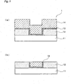
- An example of a sectional drawing of the semiconductor substrate is shown in Fig. 1(a).
- the semiconductor substrate 1 shown in Fig. 1(a) consists of a base substrate 11 made of, for example, silicon, an insulating film 12, a barrier metal film 13 and a metal film 14 for forming a wiring portion.
- a chemical mechanical polishing aqueous dispersion for use in the chemical mechanical polishing contains abrasives, an organic acid and an oxidizing agent, and may further contain an inorganic acid and a complexing agent, when needed.
- the cleaning composition of the invention exerts its maximum effect.
- abrasives examples include inorganic oxides, organic particles and organic-inorganic composite particles. Of these, preferable are silica, ceria, alumina and organic-inorganic composite particles.
- the "organic-inorganic composite particles” mean particles wherein an organic particle and an inorganic particle are united by the electrostatic or chemical action.
- the organic acid is preferably an organic acid having two or more carboxyl groups in one molecule, and examples of such organic acids include oxalic acid, maleic acid, malic acid, succinic acid and citric acid.
- oxidizing agents examples include hydrogen peroxide and ammonium persulfate.
- Examples of the inorganic acids include nitric acid and sulfuric acid.
- the complexing agents include a monocyclic compound having a five-membered heterocyclic ring or a six-membered heterocyclic ring having at least one nitrogen atom, and a compound having a condensed ring constituted of a benzene ring or a naphthalene ring and a five-membered heterocyclic ring or a six-membered heterocyclic ring having at least one nitrogen atom.
- Examples of the monocyclic compounds include quinolinic acid and pyridinecarboxylic acid.
- Examples of the compound having a condensed ring include a compound having a condensed ring structure selected from a quinoline structure, an isoquinoline structure, a benzotriazole structure, a benzimidazole structure, an indole structure, an isoindole structure, a quinazoline structure, a cinnoline structure, a quinoxaline structure, a phthalazine structure and an acridine structure.
- Preferable is a compound having a quinoline structure, a benzotriazole structure or a benzimidazole structure.
- Specific examples of the compounds having a condensed ring include quinaldinic acid, quinolinol, benzotriazole, benzimidazole, hydroxybenzotriazole and carboxybenzotriazole.
- the complexing agent for use in the invention is preferably quinolinic acid, quinaldinic acid, quinolinol or benzotriazole.
- the polishing aqueous dispersion When the excess barrier metal and metallic wiring material are removed in the present invention, it is not necessary to use the polishing aqueous dispersion throughout the chemical mechanical polishing step, and the polishing aqueous dispersion has only to be used in a part of the polishing step, preferably in the final stage of the polishing step.
- the cleaning composition of the invention sufficiently exerts its effect on the semiconductor substrate having been polished using the polishing aqueous dispersion in a part of the polishing step, preferably in the final stage of the polishing step.
- the semiconductor substrate from which the excess barrier metal and metallic wiring material have been removed in the chemical mechanical polishing step has a section shown in, for example, Fig. 1(b).
- abrasives, polishing dust, metal ions and the like (not shown) often remain on the insulating film 12 and the metal film 14 for forming a wiring portion of the polished surface.
- the method for cleaning a semiconductor substrate according to the invention is a method to remove such residues from the semiconductor substrate surface by the use of the cleaning composition.
- the cleaning method of the invention can be carried out similarly to a conventional method, such as on-table cleaning, brush-scrub cleaning or roll cleaning, except for using the cleaning composition of the invention.
- the cleaning method exemplified above may be carried out only once, but may be carried out two or more times. When cleaning is carried out two or more times, the same method may be repeated, or different methods may be used in combination. Further, cleaning may be carried out plural times combining the cleaning method of the invention using the cleaning composition of the invention with a conventional cleaning method, such as a cleaning method using pure water. In this case, the cleaning method of the invention and the conventional cleaning method may be carried out in any order.
- the cleaning conditions can be arbitrarily selected.
- the head rotating speed is in the range of preferably 10 to 150 rpm, more preferably 20 to 100 rpm;
- the head load is in the range of preferably 5 to 350 g/cm 2 , more preferably 10 to 210 g/cm 2 ;
- the table rotating speed is in the range of preferably 10 to 150 rpm, more preferably 20 to 100 rpm;
- the feed rate of the cleaning composition is in the range of preferably 50 to 400 ml/min, more preferably 100 to 300 ml/min;
- the cleaning time is in the range of preferably 5 to 120 seconds, more preferably 10 to 100 seconds.
- the cleaning of the semiconductor substrate is carried out by slipping the substrate between two brushes or two rolls.
- the rotating speed of each brush or each roll can be set in same speed, or when needed, can be set in different speed.
- the cleaning conditions are independently set depending on a cleaning apparatus or cleaning unit, the cleaning conditions which are applied for the cleaning process using a common cleaning agent can be applied for the cleaning process according to the present invention.
- the rotating speed of brush or roll is in the range of preferably 10 to 500 rpm, more preferably 30 to 300 rpm; the substrate rotating speed is in the range of preferably 10 to 300 rpm, more preferably 30 to 200 rpm; the feed rate of the cleaning composition is in the range of preferably 10 to 500 ml/min, more preferably 50 to 300 ml/min; and the cleaning time is in the range of preferably 5 to 120 seconds, more preferably 10 to 100 seconds.
- a cleaning composition which exhibits high ability to remove impurities, such as residual abrasives, residual polishing dust and metal ions, without corroding a metal wiring portion when it is used to remove contamination of a surface of a semiconductor substrate having the metal wiring portion after the chemical mechanical polishing of the semiconductor substrate.
- crosslinked organic polymer particles (1) a water dispersion containing organic polymer particles (1) (referred to as "crosslinked organic polymer particles (1)" hereinafter) having a carboxyl group and a crosslinked structure and having an average dispersed particle diameter of 210 nm was obtained. Then, ion-exchanged water was added to the water dispersion to adjust the content of the crosslinked organic polymer particles (1) to 10% by mass.
- a water dispersion containing organic polymer particles (2) (referred to as "crosslinked organic polymer particles (2)" hereinafter) having a carboxyl group and a crosslinked structure and having an average dispersed particle diameter of 190 nm was obtained in the same manner as in Preparation Example A1, except that 5 parts by mass of methacrylic acid, 10 parts by mass of trimethylolpropane triacrylate, 35 parts by mass of styrene and 50 parts by mass of methyl methacrylate were used as monomers. Then, ion-exchanged water was added to the water dispersion to adjust the content of the crosslinked organic polymer particles (2) to 10% by mass.
- a water dispersion containing organic polymer particles (3) (referred to as "crosslinked organic polymer particles (3)" hereinafter) having a carboxyl group and a crosslinked structure and having an average dispersed particle diameter of 250 nm was obtained in the same manner as in Preparation Example A1, except that 5 parts by mass of acrylic acid, 10 parts by mass of divinylbenzene, 45 parts by mass of styrene and 40 parts by mass of methyl methacrylate were used as monomers. Then, ion-exchanged water was added to the water dispersion to adjust the content of the crosslinked organic polymer particles (3) to 10% by mass.
- a water dispersion containing organic polymer particles (a) (referred to as "non-crosslinked organic polymer particles (a)" hereinafter) having a carboxyl group, having no crosslinked structure and having an average dispersed particle diameter of 200 nm was obtained in the same manner as in Preparation Example A1, except that 5 parts by mass of methacrylic acid and 95 parts by mass of styrene were used as monomers. Then, ion-exchanged water was added to the water dispersion to adjust the content of the non-crosslinked organic polymer particles (a) to 10% by mass.
- the water dispersion containing the crosslinked organic polymer particles shown in Table 2 In a polyethylene container, the water dispersion containing the crosslinked organic polymer particles shown in Table 2, said dispersion being prepared in the above preparation example, in the amount shown in Table 2 in terms of the crosslinked organic polymer particles and a surfactant of the type and in the amount shown in Table 2 were placed, and they were stirred for 15 minutes. Then, ion-exchanged water was added to the mixture so that the total amount of all the constituents should become 100 parts by mass, and then the mixture was filtered through a filter having a pore size of 5 ⁇ m to give each of cleaning compositions (1) to (3).
- the pH values of these compositions are set forth in Table 2.
- the water dispersion containing the crosslinked organic polymer particles shown in Table 2 In a polyethylene container, the water dispersion containing the crosslinked organic polymer particles shown in Table 2, said dispersion being prepared in the above preparation example, in the amount shown in Table 2 in terms of the crosslinked organic polymer particles, a surfactant of the type and in the amount shown in Table 2 and an organic acid of the type and in the amount shown in Table 2 were placed, and they were stirred for 15 minutes. Then, ion-exchanged water was added to the mixture so that the total amount of all the constituents should become 100 parts by mass, and then the mixture was filtered through a filter having a pore size of 5 ⁇ m to give each of cleaning compositions (4) to (6).
- the pH values of these compositions are set forth in Table 2.
- the water dispersion containing the crosslinked organic polymer particles shown in Table 2 said dispersion being prepared in the above preparation example, in the amount shown in Table 2 in terms of the crosslinked organic polymer particles, a surfactant of the type and in the amount shown in Table 2, an organic acid of the type and in the amount shown in Table 2 and a complexing agent of the type and in the amount shown in Table 2 were placed, and they were stirred for 15 minutes. Then, ion-exchanged water was added to the mixture so that the total amount of all the constituents should become 100 parts by mass, and then the mixture was filtered through a filter having a pore size of 5 ⁇ m to give each of cleaning compositions (7) to (10).
- the pH values of these compositions are set forth in Table 2.
- the pH value of this composition is set forth in Table 2.
- a rotary dispersing apparatus 70 parts by mass of ammonia water having a concentration of 25% by mass, 40 parts by mass of ion-exchanged water, 170 parts by mass of ethanol and 20 parts by mass of tetraethoxysilane were placed, and they were heated up to 60°C with rotary stirring at 180 rpm, followed by further stirring at 60°C for 2 hours. Subsequently, the resulting mixture was cooled to room temperature, and then an operation of removing ethanol by the use of a rotary evaporator with adding ion-exchanged water at 80°C was repeated several times to give a water dispersion containing 20% by mass of colloidal silica (1).
- the colloidal silica (1) contained in the water dispersion had an average primary particle diameter of 25 nm and an average secondary particle diameter of 40 nm.
- a water dispersion containing 20% by mass of colloidal silica (2) was obtained in the same manner as in Preparation Example B1, except that the amount of ethanol used was changed to 190 parts by mass from 170 parts by mass and the amount of tetraethoxysilane used was changed to 35 parts by mass from 20 parts by mass.
- the colloidal silica (2) contained in the water dispersion had an average primary particle diameter of 50 nm and an average secondary particle diameter of 75 nm.
- a potassium hydroxide aqueous solution of 20% by mass was added to the resulting mixture.
- the mixture was diluted with ion-exchanged water and filtered through a depth cartridge filter having a pore size of 5 ⁇ m to give a water dispersion containing 30% by mass of the fumed silica.
- the silica contained in the water dispersion had an average dispersed particle diameter of 52 nm.
- a water dispersion containing 10% by mass of organic abrasives (2) having an average dispersed particle diameter of 190 nm was obtained in the same manner as in Preparation Example B5, except that 4 parts by mass of methacrylic acid, 91 parts by mass of styrene and 5 parts by mass of divinylbenzene were used as monomers.
- the water dispersion containing the abrasives shown in Table 3 said dispersion being prepared in the above preparation example, in the amount shown in Table 3 in terms of the abrasives, an organic acid of the type and in the amount shown in Table 3, a complexing agent of the type and in the amount shown in Table 3 and an oxidizing agent of the type and in the amount shown in Table 3 were placed in this order, and they were stirred for 15 minutes.
- a pH adjuster shown in Table 3 was added so that the pH of a resultant chemical mechanical polishing aqueous dispersion became the value shown in Table 3, and then ion-exchanged water was further added so that the total amount of all the constituents became 100 parts by weight. Then, the mixture was filtered through a filter having a pore size of 5 ⁇ m to give each of chemical mechanical polishing aqueous dispersions (1) to (10).
- the pH values of these polishing aqueous dispersions are set forth in Table 3.
- the film had a dielectric constant of 1.98, an elastic modulus of 3 GPa and a porosity of 15%.
- Copper nitrate was dissolved in ultra-pure water to prepare a solution containing copper ion in a concentration of 100 ppb.
- an 8-inch p-type silicon wafer manufactured by Shin-Etsu Semiconductor Co., Ltd.
- the metal contamination of the substrate was quantitatively determined by a total reflection fluorescent X-ray method using "TREX610T” manufactured by Technos Co., Ltd., and as a result, a copper atom adhered in an amount of 2 ⁇ 10 13 atom/cm 2 .
- step (1-1) the surface of the substrate obtained after the polishing was subjected to on-table cleaning and then brush-scrub cleaning under the following conditions. This is referred to as "two-stage cleaning" hereinafter.
- the film thickness of the insulating film was measured by the use of an optical interferotype measuring instrument "FPT500” (manufactured by SENTEC Co.), and from a difference between the resulting values and the polishing time, a removal rate was calculated. As a result, the removal rate was 1,200 ⁇ /min. Further, after the cleaning, the whole surface of the insulating film was observed by the use of a wafer surface inspection system "Surfscan SP1" (manufactured by KLA Tencor Co.), and as a result, the number of surface defects was 8 defects/surface.
- the "surface defects” used herein include residual abrasives, water mark (nearly circular tarnished portion like a stain though the cause of occurrence is unknown), and the like.
- the substrate contaminated by a metal was subjected to two-stage cleaning in the same manner as in the above step "(1-2) Cleaning of insulating film” by the use of a chemical mechanical polishing apparatus "EPO112" (manufactured by Ebara Corp.).
- the metal contamination of the substrate was quantitatively determined by a total reflection fluorescent X-ray method using "TREX610T” manufactured by Technos Co., Ltd., and as a result, the amount of the residual copper atom was 5 ⁇ 10 11 atom/cm 2 .
- the surface of the substrate obtained after the polishing was subjected to two-stage cleaning in the same manner as in Example 1, except that the cleaning agents shown in Table 4 were used instead of the cleaning compositions (1) and (11).
- the substrate contaminated by a metal said substrate being prepared in the process (D) was subjected to two-step cleaning in the same manner as in Example 1, except that the cleaning agents shown in Table 4 were used instead of the cleaning compositions (1) and (11).
- a substrate with a copper wiring pattern (available from International SEMATECH, Model Number: 854LKD003) was subjected to two-stage chemical mechanical polishing under the following conditions using a chemical mechanical polishing apparatus "EPO112" (manufactured by Ebara Corp.).
- a substrate with a copper wiring pattern (854LKD003) was subjected to two-stage chemical mechanical polishing and then subjected to two-stage cleaning in the same manner as in Example 14, except that ultra-pure water was used as a cleaning agent for on-table cleaning and the cleaning composition (11) was used as a cleaning agent for brush-scrub cleaning. After the cleaning, the whole surface of the substrate was observed in the same manner as in Example 14, and as a result, the number of surface defects was 162 defects/surface. Further, dishing of the wiring portion of 100 ⁇ m wide on the substrate was 310 ⁇ .
- the cleaning composition which comprises organic polymer particles (A) having a crosslinked structure and a surfactant (B) and is used after chemical mechanical polishing.
- the cleaning method of a semiconductor substrate is a method for cleaning semiconductor substrate given after chemical mechanical polishing, by the use of the cleaning composition.
- the process for manufacturing a semiconductor device including a step of chemically and mechanically polishing a semiconductor substrate and a step of cleaning the semiconductor substrate obtained after the chemical mechanical polishing, by the cleaning method.
Landscapes
- Chemical & Material Sciences (AREA)
- Life Sciences & Earth Sciences (AREA)
- Engineering & Computer Science (AREA)
- Chemical Kinetics & Catalysis (AREA)
- Oil, Petroleum & Natural Gas (AREA)
- Wood Science & Technology (AREA)
- Organic Chemistry (AREA)
- Detergent Compositions (AREA)
- Cleaning Or Drying Semiconductors (AREA)
Applications Claiming Priority (2)
| Application Number | Priority Date | Filing Date | Title |
|---|---|---|---|
| JP2004033158 | 2004-02-10 | ||
| JP2004033158 | 2004-02-10 |
Publications (1)
| Publication Number | Publication Date |
|---|---|
| EP1569267A1 true EP1569267A1 (de) | 2005-08-31 |
Family
ID=34747397
Family Applications (1)
| Application Number | Title | Priority Date | Filing Date |
|---|---|---|---|
| EP05002697A Withdrawn EP1569267A1 (de) | 2004-02-10 | 2005-02-09 | Reinigungsmittel, Verfahren zur Reinigung eines Halbleitersubstrats und Verfahren zu Herstellung von Halbleiterbauelementen |
Country Status (5)
| Country | Link |
|---|---|
| US (1) | US7498294B2 (de) |
| EP (1) | EP1569267A1 (de) |
| KR (2) | KR100775199B1 (de) |
| CN (1) | CN1654617A (de) |
| TW (1) | TWI262552B (de) |
Cited By (3)
| Publication number | Priority date | Publication date | Assignee | Title |
|---|---|---|---|---|
| EP1997129A4 (de) * | 2006-02-03 | 2010-03-17 | Advanced Tech Materials | Nach-cmp-restentfernungszusammensetzung mit niedrigem ph und verwendungsverfahren |
| CN106133104A (zh) * | 2014-03-28 | 2016-11-16 | 福吉米株式会社 | 研磨用组合物 |
| KR20220095210A (ko) * | 2019-12-26 | 2022-07-06 | 후지필름 가부시키가이샤 | 세정액, 세정 방법 |
Families Citing this family (46)
| Publication number | Priority date | Publication date | Assignee | Title |
|---|---|---|---|---|
| US7799141B2 (en) * | 2003-06-27 | 2010-09-21 | Lam Research Corporation | Method and system for using a two-phases substrate cleaning compound |
| US8316866B2 (en) * | 2003-06-27 | 2012-11-27 | Lam Research Corporation | Method and apparatus for cleaning a semiconductor substrate |
| US8522801B2 (en) * | 2003-06-27 | 2013-09-03 | Lam Research Corporation | Method and apparatus for cleaning a semiconductor substrate |
| US20040261823A1 (en) * | 2003-06-27 | 2004-12-30 | Lam Research Corporation | Method and apparatus for removing a target layer from a substrate using reactive gases |
| US7737097B2 (en) * | 2003-06-27 | 2010-06-15 | Lam Research Corporation | Method for removing contamination from a substrate and for making a cleaning solution |
| US7648584B2 (en) | 2003-06-27 | 2010-01-19 | Lam Research Corporation | Method and apparatus for removing contamination from substrate |
| US7862662B2 (en) * | 2005-12-30 | 2011-01-04 | Lam Research Corporation | Method and material for cleaning a substrate |
| US8522799B2 (en) * | 2005-12-30 | 2013-09-03 | Lam Research Corporation | Apparatus and system for cleaning a substrate |
| US8043441B2 (en) | 2005-06-15 | 2011-10-25 | Lam Research Corporation | Method and apparatus for cleaning a substrate using non-Newtonian fluids |
| US8323420B2 (en) | 2005-06-30 | 2012-12-04 | Lam Research Corporation | Method for removing material from semiconductor wafer and apparatus for performing the same |
| US7416370B2 (en) * | 2005-06-15 | 2008-08-26 | Lam Research Corporation | Method and apparatus for transporting a substrate using non-Newtonian fluid |
| US7568490B2 (en) * | 2003-12-23 | 2009-08-04 | Lam Research Corporation | Method and apparatus for cleaning semiconductor wafers using compressed and/or pressurized foams, bubbles, and/or liquids |
| TW200717635A (en) * | 2005-09-06 | 2007-05-01 | Komatsu Denshi Kinzoku Kk | Polishing method for semiconductor wafer |
| CN1982426B (zh) * | 2005-12-16 | 2011-08-03 | 安集微电子(上海)有限公司 | 用于半导体晶片清洗的缓蚀剂体系 |
| SG154438A1 (en) * | 2005-12-30 | 2009-08-28 | Lam Res Corp | Cleaning compound and method and system for using the cleaning compound |
| GB0607047D0 (en) * | 2006-04-07 | 2006-05-17 | Univ Leeds | Novel cleaning method |
| JP4912791B2 (ja) * | 2006-08-21 | 2012-04-11 | Jsr株式会社 | 洗浄用組成物、洗浄方法及び半導体装置の製造方法 |
| JP4777197B2 (ja) * | 2006-09-11 | 2011-09-21 | 富士フイルム株式会社 | 洗浄液及びそれを用いた洗浄方法 |
| US20080076688A1 (en) * | 2006-09-21 | 2008-03-27 | Barnes Jeffrey A | Copper passivating post-chemical mechanical polishing cleaning composition and method of use |
| US20080148595A1 (en) * | 2006-12-20 | 2008-06-26 | Lam Research Corporation | Method and apparatus for drying substrates using a surface tensions reducing gas |
| US7897213B2 (en) * | 2007-02-08 | 2011-03-01 | Lam Research Corporation | Methods for contained chemical surface treatment |
| WO2009032460A1 (en) * | 2007-08-02 | 2009-03-12 | Advanced Technology Materials, Inc. | Non-fluoride containing composition for the removal of residue from a microelectronic device |
| US8822396B2 (en) | 2007-08-22 | 2014-09-02 | Daikin Industries, Ltd. | Solution for removing residue after semiconductor dry process and method of removing the residue using the same |
| US8084406B2 (en) * | 2007-12-14 | 2011-12-27 | Lam Research Corporation | Apparatus for particle removal by single-phase and two-phase media |
| TWI460557B (zh) * | 2008-03-07 | 2014-11-11 | 和光純藥工業股份有限公司 | 半導體表面用處理劑組成物及使用半導體表面用處理劑組成物之半導體表面處理方法 |
| CN101555029B (zh) * | 2008-04-09 | 2011-05-04 | 清华大学 | 铝酸锌纳米材料的制备方法 |
| GB201006076D0 (en) | 2010-04-12 | 2010-05-26 | Xeros Ltd | Novel cleaning apparatus and method |
| US8883701B2 (en) | 2010-07-09 | 2014-11-11 | Air Products And Chemicals, Inc. | Method for wafer dicing and composition useful thereof |
| GB201015277D0 (en) | 2010-09-14 | 2010-10-27 | Xeros Ltd | Novel cleaning method |
| GB201100627D0 (en) | 2011-01-14 | 2011-03-02 | Xeros Ltd | Improved cleaning method |
| GB201100918D0 (en) | 2011-01-19 | 2011-03-02 | Xeros Ltd | Improved drying method |
| CN103451748B (zh) * | 2012-05-28 | 2016-01-13 | 中国科学院宁波材料技术与工程研究所 | 一种聚丙烯腈原丝纺丝喷丝板的清洗方法 |
| GB201212098D0 (en) | 2012-07-06 | 2012-08-22 | Xeros Ltd | New cleaning material |
| GB201319782D0 (en) | 2013-11-08 | 2013-12-25 | Xeros Ltd | Cleaning method and apparatus |
| GB201320784D0 (en) | 2013-11-25 | 2014-01-08 | Xeros Ltd | Improved cleaning Apparatus and method |
| CN104051238A (zh) * | 2014-05-20 | 2014-09-17 | 上海华力微电子有限公司 | 去除双大马士革工艺中聚合物残留的方法 |
| JP6112330B1 (ja) * | 2016-05-10 | 2017-04-12 | Jsr株式会社 | 半導体洗浄用組成物および洗浄方法 |
| US10319605B2 (en) | 2016-05-10 | 2019-06-11 | Jsr Corporation | Semiconductor treatment composition and treatment method |
| US10954479B2 (en) | 2016-07-26 | 2021-03-23 | Fujimi Incorporated | Composition for surface treatment and surface treatment method using the same |
| JP6697362B2 (ja) * | 2016-09-23 | 2020-05-20 | 株式会社フジミインコーポレーテッド | 表面処理組成物、ならびにこれを用いた表面処理方法および半導体基板の製造方法 |
| WO2018168207A1 (ja) | 2017-03-14 | 2018-09-20 | 株式会社フジミインコーポレーテッド | 表面処理組成物、その製造方法、およびこれを用いた表面処理方法 |
| US11060051B2 (en) | 2018-10-12 | 2021-07-13 | Fujimi Incorporated | Composition for rinsing or cleaning a surface with ceria particles adhered |
| JP7680366B2 (ja) * | 2019-04-09 | 2025-05-20 | ビーエーエスエフ ソシエタス・ヨーロピア | 50nm以下のライン間寸法を有するパターン化材料を処理する際のパターンの崩壊を回避するための、アンモニア活性化シロキサンを含む組成物 |
| JP2024501226A (ja) * | 2020-12-21 | 2024-01-11 | フジフイルム エレクトロニック マテリアルズ ユー.エス.エー., インコーポレイテッド | 化学機械研磨組成物及びその使用方法 |
| CN115870276B (zh) * | 2022-11-16 | 2024-12-03 | 富乐德科技发展(大连)有限公司 | 去除半导体蚀刻设备esc静电吸附盘表面高温沉积的硅、氧、氮化钛及氟化物沉积膜工艺 |
| CN115799162A (zh) * | 2023-01-29 | 2023-03-14 | 合肥晶合集成电路股份有限公司 | 一种半导体结构的制备方法 |
Citations (4)
| Publication number | Priority date | Publication date | Assignee | Title |
|---|---|---|---|---|
| JPH11222600A (ja) * | 1997-11-27 | 1999-08-17 | Toshiba Corp | 洗浄液および半導体装置の製造方法 |
| EP1020501A2 (de) * | 1999-01-18 | 2000-07-19 | Kabushiki Kaisha Toshiba | Wässrige Dispersion zum chemisch-mechanischen Polieren, Verfahren zum Polieren von Halbleiterscheibenoberflächen und Verfahren zur Herstellung einer Halbleiteranordnung |
| US6440856B1 (en) * | 1999-09-14 | 2002-08-27 | Jsr Corporation | Cleaning agent for semiconductor parts and method for cleaning semiconductor parts |
| US20030109413A1 (en) * | 2001-07-11 | 2003-06-12 | Cedric Geffroy | Process for cleaning a surface using an aqueous composition containing a dispersed polymer |
Family Cites Families (6)
| Publication number | Priority date | Publication date | Assignee | Title |
|---|---|---|---|---|
| JP3219020B2 (ja) | 1996-06-05 | 2001-10-15 | 和光純薬工業株式会社 | 洗浄処理剤 |
| JP2001269859A (ja) * | 2000-03-27 | 2001-10-02 | Jsr Corp | 化学機械研磨用水系分散体 |
| EP1211024A3 (de) * | 2000-11-30 | 2004-01-02 | JSR Corporation | Polierverfahren |
| US20020173243A1 (en) * | 2001-04-05 | 2002-11-21 | Costas Wesley D. | Polishing composition having organic polymer particles |
| JP3692109B2 (ja) | 2002-10-24 | 2005-09-07 | 株式会社東芝 | 半導体装置の製造方法 |
| US7005382B2 (en) * | 2002-10-31 | 2006-02-28 | Jsr Corporation | Aqueous dispersion for chemical mechanical polishing, chemical mechanical polishing process, production process of semiconductor device and material for preparing an aqueous dispersion for chemical mechanical polishing |
-
2005
- 2005-02-03 CN CNA2005100016782A patent/CN1654617A/zh active Pending
- 2005-02-05 TW TW094103983A patent/TWI262552B/zh not_active IP Right Cessation
- 2005-02-07 KR KR1020050011102A patent/KR100775199B1/ko not_active Expired - Fee Related
- 2005-02-09 EP EP05002697A patent/EP1569267A1/de not_active Withdrawn
- 2005-02-09 US US11/052,910 patent/US7498294B2/en not_active Expired - Lifetime
-
2007
- 2007-08-24 KR KR1020070085661A patent/KR20070091095A/ko not_active Withdrawn
Patent Citations (4)
| Publication number | Priority date | Publication date | Assignee | Title |
|---|---|---|---|---|
| JPH11222600A (ja) * | 1997-11-27 | 1999-08-17 | Toshiba Corp | 洗浄液および半導体装置の製造方法 |
| EP1020501A2 (de) * | 1999-01-18 | 2000-07-19 | Kabushiki Kaisha Toshiba | Wässrige Dispersion zum chemisch-mechanischen Polieren, Verfahren zum Polieren von Halbleiterscheibenoberflächen und Verfahren zur Herstellung einer Halbleiteranordnung |
| US6440856B1 (en) * | 1999-09-14 | 2002-08-27 | Jsr Corporation | Cleaning agent for semiconductor parts and method for cleaning semiconductor parts |
| US20030109413A1 (en) * | 2001-07-11 | 2003-06-12 | Cedric Geffroy | Process for cleaning a surface using an aqueous composition containing a dispersed polymer |
Non-Patent Citations (1)
| Title |
|---|
| PATENT ABSTRACTS OF JAPAN vol. 1999, no. 13 30 November 1999 (1999-11-30) * |
Cited By (5)
| Publication number | Priority date | Publication date | Assignee | Title |
|---|---|---|---|---|
| EP1997129A4 (de) * | 2006-02-03 | 2010-03-17 | Advanced Tech Materials | Nach-cmp-restentfernungszusammensetzung mit niedrigem ph und verwendungsverfahren |
| CN106133104A (zh) * | 2014-03-28 | 2016-11-16 | 福吉米株式会社 | 研磨用组合物 |
| EP3124570A4 (de) * | 2014-03-28 | 2017-02-08 | Fujimi Incorporated | Polierzusammensetzung |
| US10144907B2 (en) | 2014-03-28 | 2018-12-04 | Fujimi Incorporated | Polishing composition |
| KR20220095210A (ko) * | 2019-12-26 | 2022-07-06 | 후지필름 가부시키가이샤 | 세정액, 세정 방법 |
Also Published As
| Publication number | Publication date |
|---|---|
| US20050176606A1 (en) | 2005-08-11 |
| KR100775199B1 (ko) | 2007-11-12 |
| US7498294B2 (en) | 2009-03-03 |
| KR20070091095A (ko) | 2007-09-07 |
| TW200527519A (en) | 2005-08-16 |
| TWI262552B (en) | 2006-09-21 |
| KR20060041794A (ko) | 2006-05-12 |
| CN1654617A (zh) | 2005-08-17 |
Similar Documents
| Publication | Publication Date | Title |
|---|---|---|
| US7498294B2 (en) | Cleaning composition, method for cleaning semiconductor substrate, and process for manufacturing semiconductor device | |
| JP4912791B2 (ja) | 洗浄用組成物、洗浄方法及び半導体装置の製造方法 | |
| JP4516176B2 (ja) | 電子材料用基板洗浄液 | |
| US6546939B1 (en) | Post clean treatment | |
| JP4821122B2 (ja) | 洗浄用組成物、半導体基板の洗浄方法および半導体装置の製造方法 | |
| JP5408437B2 (ja) | 化学機械研磨用水系分散体、および該分散体を調製するためのキット、該キットを用いた化学機械研磨用水系分散体の調製方法、ならびに半導体装置の化学機械研磨方法 | |
| CN108431931B (zh) | 用于化学机械抛光后清洁的组合物 | |
| JP2010258014A (ja) | 洗浄用組成物および洗浄方法 | |
| WO2012051787A1 (zh) | 一种化学机械抛光液 | |
| CN108473918A (zh) | 用于化学机械抛光后清洁的组合物 | |
| JP2022054189A (ja) | 表面処理組成物、表面処理組成物の製造方法、表面処理方法、および半導体基板の製造方法 | |
| JP2004128475A (ja) | 化学機械研磨用水系分散体および半導体装置の製造方法 | |
| JP2025540092A (ja) | 研磨組成物及びその使用の方法 | |
| TW463256B (en) | Process for removing contaminant from a surface and composition useful therefor | |
| JP5333740B2 (ja) | 化学機械研磨用水系分散体およびその製造方法、ならびに化学機械研磨方法 | |
| JP7299102B2 (ja) | 中間原料、ならびにこれを用いた研磨用組成物および表面処理組成物 | |
| JP2009224771A (ja) | 化学機械研磨用水系分散体およびその製造方法、ならびに化学機械研磨方法 | |
| JP5344136B2 (ja) | 化学機械研磨用水系分散体、および該分散体の調製方法、ならびに半導体装置の化学機械研磨方法 | |
| CN115992031A (zh) | 化学机械研磨后清洗液组合物 | |
| US20040140288A1 (en) | Wet etch of titanium-tungsten film | |
| JP2004022986A (ja) | 化学的機械的研磨後の洗浄液 | |
| JP5413569B2 (ja) | 化学機械研磨用水系分散体およびその製造方法、ならびに化学機械研磨方法 | |
| WO2023084861A1 (ja) | セリウム化合物除去用洗浄液、洗浄方法及び半導体ウェハの製造方法 | |
| JP2010118377A (ja) | 化学機械研磨用水系分散体、および該分散体の調製方法、ならびに半導体装置の化学機械研磨方法 | |
| JP2009224767A (ja) | 化学機械研磨用水系分散体およびその製造方法、ならびに化学機械研磨方法 |
Legal Events
| Date | Code | Title | Description |
|---|---|---|---|
| PUAI | Public reference made under article 153(3) epc to a published international application that has entered the european phase |
Free format text: ORIGINAL CODE: 0009012 |
|
| AK | Designated contracting states |
Kind code of ref document: A1 Designated state(s): AT BE BG CH CY CZ DE DK EE ES FI FR GB GR HU IE IS IT LI LT LU MC NL PL PT RO SE SI SK TR |
|
| AX | Request for extension of the european patent |
Extension state: AL BA HR LV MK YU |
|
| 17P | Request for examination filed |
Effective date: 20050728 |
|
| AKX | Designation fees paid |
Designated state(s): DE FR GB IT |
|
| STAA | Information on the status of an ep patent application or granted ep patent |
Free format text: STATUS: THE APPLICATION IS DEEMED TO BE WITHDRAWN |
|
| 18D | Application deemed to be withdrawn |
Effective date: 20121206 |