EP1567306B1 - Transparente mikroporöse materialien für cmp - Google Patents
Transparente mikroporöse materialien für cmp Download PDFInfo
- Publication number
- EP1567306B1 EP1567306B1 EP03809403A EP03809403A EP1567306B1 EP 1567306 B1 EP1567306 B1 EP 1567306B1 EP 03809403 A EP03809403 A EP 03809403A EP 03809403 A EP03809403 A EP 03809403A EP 1567306 B1 EP1567306 B1 EP 1567306B1
- Authority
- EP
- European Patent Office
- Prior art keywords
- polishing pad
- polishing
- substrate
- pad substrate
- porous material
- Prior art date
- Legal status (The legal status is an assumption and is not a legal conclusion. Google has not performed a legal analysis and makes no representation as to the accuracy of the status listed.)
- Expired - Lifetime
Links
- 239000012229 microporous material Substances 0.000 title 1
- 238000005498 polishing Methods 0.000 claims abstract description 205
- 239000000758 substrate Substances 0.000 claims abstract description 89
- 239000011148 porous material Substances 0.000 claims abstract description 71
- 238000002834 transmittance Methods 0.000 claims abstract description 13
- 238000007517 polishing process Methods 0.000 claims abstract description 12
- 239000002952 polymeric resin Substances 0.000 claims description 43
- 229920003002 synthetic resin Polymers 0.000 claims description 43
- 239000000203 mixture Substances 0.000 claims description 14
- 239000004433 Thermoplastic polyurethane Substances 0.000 claims description 12
- 229920002803 thermoplastic polyurethane Polymers 0.000 claims description 12
- 229920001577 copolymer Polymers 0.000 claims description 10
- 238000001514 detection method Methods 0.000 claims description 10
- -1 polyethylenes Polymers 0.000 claims description 9
- 238000011065 in-situ storage Methods 0.000 claims description 8
- 229920000515 polycarbonate Polymers 0.000 claims description 6
- 239000004417 polycarbonate Substances 0.000 claims description 6
- 239000011800 void material Substances 0.000 claims description 6
- 229920001778 nylon Polymers 0.000 claims description 5
- 239000004642 Polyimide Substances 0.000 claims description 4
- 229920001971 elastomer Polymers 0.000 claims description 4
- 229920001721 polyimide Polymers 0.000 claims description 4
- 239000005060 rubber Substances 0.000 claims description 4
- 239000004698 Polyethylene Substances 0.000 claims description 3
- 239000004793 Polystyrene Substances 0.000 claims description 3
- 229920003235 aromatic polyamide Polymers 0.000 claims description 3
- 229910044991 metal oxide Inorganic materials 0.000 claims description 3
- 150000004706 metal oxides Chemical class 0.000 claims description 3
- 229920003229 poly(methyl methacrylate) Polymers 0.000 claims description 3
- 229920000412 polyarylene Polymers 0.000 claims description 3
- 229920000573 polyethylene Polymers 0.000 claims description 3
- 229920002223 polystyrene Polymers 0.000 claims description 3
- 229920001343 polytetrafluoroethylene Polymers 0.000 claims description 3
- 239000004810 polytetrafluoroethylene Substances 0.000 claims description 3
- 229920002451 polyvinyl alcohol Polymers 0.000 claims description 3
- 235000019422 polyvinyl alcohol Nutrition 0.000 claims description 3
- 229920002725 thermoplastic elastomer Polymers 0.000 claims description 3
- 229920002397 thermoplastic olefin Polymers 0.000 claims description 2
- 238000000034 method Methods 0.000 description 41
- 239000007789 gas Substances 0.000 description 29
- 229920000642 polymer Polymers 0.000 description 27
- 239000002904 solvent Substances 0.000 description 21
- 230000008569 process Effects 0.000 description 20
- 239000010410 layer Substances 0.000 description 19
- 239000000463 material Substances 0.000 description 19
- 229920002635 polyurethane Polymers 0.000 description 17
- 239000004814 polyurethane Substances 0.000 description 17
- 239000007787 solid Substances 0.000 description 15
- 235000012431 wafers Nutrition 0.000 description 14
- 239000000975 dye Substances 0.000 description 11
- 239000002245 particle Substances 0.000 description 11
- 239000000243 solution Substances 0.000 description 10
- 230000015572 biosynthetic process Effects 0.000 description 6
- 230000003993 interaction Effects 0.000 description 6
- 229920002959 polymer blend Polymers 0.000 description 6
- 229920000098 polyolefin Polymers 0.000 description 6
- 238000000518 rheometry Methods 0.000 description 6
- 239000004065 semiconductor Substances 0.000 description 6
- VYPSYNLAJGMNEJ-UHFFFAOYSA-N silicon dioxide Inorganic materials O=[Si]=O VYPSYNLAJGMNEJ-UHFFFAOYSA-N 0.000 description 6
- 238000001125 extrusion Methods 0.000 description 5
- 239000012530 fluid Substances 0.000 description 5
- 239000000499 gel Substances 0.000 description 5
- 230000006911 nucleation Effects 0.000 description 5
- 238000010899 nucleation Methods 0.000 description 5
- CURLTUGMZLYLDI-UHFFFAOYSA-N Carbon dioxide Chemical compound O=C=O CURLTUGMZLYLDI-UHFFFAOYSA-N 0.000 description 4
- 238000000354 decomposition reaction Methods 0.000 description 4
- 230000007423 decrease Effects 0.000 description 4
- 238000009826 distribution Methods 0.000 description 4
- 238000001746 injection moulding Methods 0.000 description 4
- 229910052751 metal Inorganic materials 0.000 description 4
- 239000002184 metal Substances 0.000 description 4
- 238000004377 microelectronic Methods 0.000 description 4
- 239000002861 polymer material Substances 0.000 description 4
- 230000005855 radiation Effects 0.000 description 4
- LFQSCWFLJHTTHZ-UHFFFAOYSA-N Ethanol Chemical compound CCO LFQSCWFLJHTTHZ-UHFFFAOYSA-N 0.000 description 3
- 229910013504 M-O-M Inorganic materials 0.000 description 3
- OKKJLVBELUTLKV-UHFFFAOYSA-N Methanol Chemical compound OC OKKJLVBELUTLKV-UHFFFAOYSA-N 0.000 description 3
- ZMXDDKWLCZADIW-UHFFFAOYSA-N N,N-Dimethylformamide Chemical compound CN(C)C=O ZMXDDKWLCZADIW-UHFFFAOYSA-N 0.000 description 3
- 229910002092 carbon dioxide Inorganic materials 0.000 description 3
- 230000008859 change Effects 0.000 description 3
- 239000003795 chemical substances by application Substances 0.000 description 3
- 239000012948 isocyanate Substances 0.000 description 3
- 239000007788 liquid Substances 0.000 description 3
- 238000004519 manufacturing process Methods 0.000 description 3
- 238000012544 monitoring process Methods 0.000 description 3
- 125000000962 organic group Chemical group 0.000 description 3
- 238000005191 phase separation Methods 0.000 description 3
- 239000002243 precursor Substances 0.000 description 3
- 235000012239 silicon dioxide Nutrition 0.000 description 3
- 239000002002 slurry Substances 0.000 description 3
- 239000000126 substance Substances 0.000 description 3
- QGZKDVFQNNGYKY-UHFFFAOYSA-N Ammonia Chemical compound N QGZKDVFQNNGYKY-UHFFFAOYSA-N 0.000 description 2
- IJGRMHOSHXDMSA-UHFFFAOYSA-N Atomic nitrogen Chemical compound N#N IJGRMHOSHXDMSA-UHFFFAOYSA-N 0.000 description 2
- 239000004215 Carbon black (E152) Substances 0.000 description 2
- HEDRZPFGACZZDS-UHFFFAOYSA-N Chloroform Chemical compound ClC(Cl)Cl HEDRZPFGACZZDS-UHFFFAOYSA-N 0.000 description 2
- JOYRKODLDBILNP-UHFFFAOYSA-N Ethyl urethane Chemical compound CCOC(N)=O JOYRKODLDBILNP-UHFFFAOYSA-N 0.000 description 2
- PXHVJJICTQNCMI-UHFFFAOYSA-N Nickel Chemical compound [Ni] PXHVJJICTQNCMI-UHFFFAOYSA-N 0.000 description 2
- 239000004677 Nylon Substances 0.000 description 2
- BOTDANWDWHJENH-UHFFFAOYSA-N Tetraethyl orthosilicate Chemical compound CCO[Si](OCC)(OCC)OCC BOTDANWDWHJENH-UHFFFAOYSA-N 0.000 description 2
- 238000005299 abrasion Methods 0.000 description 2
- 239000004964 aerogel Substances 0.000 description 2
- 150000004703 alkoxides Chemical class 0.000 description 2
- 229910052782 aluminium Inorganic materials 0.000 description 2
- 238000000071 blow moulding Methods 0.000 description 2
- 239000003054 catalyst Substances 0.000 description 2
- 230000001276 controlling effect Effects 0.000 description 2
- 238000004132 cross linking Methods 0.000 description 2
- 230000006378 damage Effects 0.000 description 2
- 230000008021 deposition Effects 0.000 description 2
- KPUWHANPEXNPJT-UHFFFAOYSA-N disiloxane Chemical class [SiH3]O[SiH3] KPUWHANPEXNPJT-UHFFFAOYSA-N 0.000 description 2
- 239000006185 dispersion Substances 0.000 description 2
- 239000011521 glass Substances 0.000 description 2
- 230000009477 glass transition Effects 0.000 description 2
- 229930195733 hydrocarbon Natural products 0.000 description 2
- 150000002430 hydrocarbons Chemical class 0.000 description 2
- 230000007062 hydrolysis Effects 0.000 description 2
- 238000006460 hydrolysis reaction Methods 0.000 description 2
- 238000002347 injection Methods 0.000 description 2
- 239000007924 injection Substances 0.000 description 2
- 238000007689 inspection Methods 0.000 description 2
- IQPQWNKOIGAROB-UHFFFAOYSA-N isocyanate group Chemical group [N-]=C=O IQPQWNKOIGAROB-UHFFFAOYSA-N 0.000 description 2
- 239000000155 melt Substances 0.000 description 2
- 238000002156 mixing Methods 0.000 description 2
- 230000003287 optical effect Effects 0.000 description 2
- 229920003023 plastic Polymers 0.000 description 2
- 239000004033 plastic Substances 0.000 description 2
- BASFCYQUMIYNBI-UHFFFAOYSA-N platinum Chemical compound [Pt] BASFCYQUMIYNBI-UHFFFAOYSA-N 0.000 description 2
- 239000010453 quartz Substances 0.000 description 2
- 230000004044 response Effects 0.000 description 2
- 229910052710 silicon Inorganic materials 0.000 description 2
- 239000000377 silicon dioxide Substances 0.000 description 2
- 238000003980 solgel method Methods 0.000 description 2
- 239000011877 solvent mixture Substances 0.000 description 2
- 238000000194 supercritical-fluid extraction Methods 0.000 description 2
- 239000002344 surface layer Substances 0.000 description 2
- 239000010936 titanium Substances 0.000 description 2
- 229910052719 titanium Inorganic materials 0.000 description 2
- XLYOFNOQVPJJNP-UHFFFAOYSA-N water Substances O XLYOFNOQVPJJNP-UHFFFAOYSA-N 0.000 description 2
- QETOCFXSZWSHLS-UHFFFAOYSA-N 1-azacyclooctadeca-1,3,5,7,9,11,13,15,17-nonaene Chemical compound C1=CC=CC=CC=CC=NC=CC=CC=CC=C1 QETOCFXSZWSHLS-UHFFFAOYSA-N 0.000 description 1
- OHMHBGPWCHTMQE-UHFFFAOYSA-N 2,2-dichloro-1,1,1-trifluoroethane Chemical compound FC(F)(F)C(Cl)Cl OHMHBGPWCHTMQE-UHFFFAOYSA-N 0.000 description 1
- UGFAIRIUMAVXCW-UHFFFAOYSA-N Carbon monoxide Chemical compound [O+]#[C-] UGFAIRIUMAVXCW-UHFFFAOYSA-N 0.000 description 1
- RYGMFSIKBFXOCR-UHFFFAOYSA-N Copper Chemical compound [Cu] RYGMFSIKBFXOCR-UHFFFAOYSA-N 0.000 description 1
- PMPVIKIVABFJJI-UHFFFAOYSA-N Cyclobutane Chemical compound C1CCC1 PMPVIKIVABFJJI-UHFFFAOYSA-N 0.000 description 1
- XDTMQSROBMDMFD-UHFFFAOYSA-N Cyclohexane Chemical compound C1CCCCC1 XDTMQSROBMDMFD-UHFFFAOYSA-N 0.000 description 1
- VGGSQFUCUMXWEO-UHFFFAOYSA-N Ethene Chemical compound C=C VGGSQFUCUMXWEO-UHFFFAOYSA-N 0.000 description 1
- 239000005977 Ethylene Substances 0.000 description 1
- YCKRFDGAMUMZLT-UHFFFAOYSA-N Fluorine atom Chemical compound [F] YCKRFDGAMUMZLT-UHFFFAOYSA-N 0.000 description 1
- 229930182559 Natural dye Natural products 0.000 description 1
- 239000004952 Polyamide Substances 0.000 description 1
- 229920005830 Polyurethane Foam Polymers 0.000 description 1
- KJTLSVCANCCWHF-UHFFFAOYSA-N Ruthenium Chemical compound [Ru] KJTLSVCANCCWHF-UHFFFAOYSA-N 0.000 description 1
- 229910052581 Si3N4 Inorganic materials 0.000 description 1
- XUIMIQQOPSSXEZ-UHFFFAOYSA-N Silicon Chemical compound [Si] XUIMIQQOPSSXEZ-UHFFFAOYSA-N 0.000 description 1
- 229910002808 Si–O–Si Inorganic materials 0.000 description 1
- 239000004115 Sodium Silicate Substances 0.000 description 1
- RTAQQCXQSZGOHL-UHFFFAOYSA-N Titanium Chemical compound [Ti] RTAQQCXQSZGOHL-UHFFFAOYSA-N 0.000 description 1
- 239000003082 abrasive agent Substances 0.000 description 1
- 239000002250 absorbent Substances 0.000 description 1
- 239000002253 acid Substances 0.000 description 1
- 150000007513 acids Chemical class 0.000 description 1
- 239000000853 adhesive Substances 0.000 description 1
- 230000001070 adhesive effect Effects 0.000 description 1
- 125000000217 alkyl group Chemical group 0.000 description 1
- XAGFODPZIPBFFR-UHFFFAOYSA-N aluminium Chemical compound [Al] XAGFODPZIPBFFR-UHFFFAOYSA-N 0.000 description 1
- 150000001412 amines Chemical class 0.000 description 1
- 229910021529 ammonia Inorganic materials 0.000 description 1
- 239000001000 anthraquinone dye Substances 0.000 description 1
- 239000002518 antifoaming agent Substances 0.000 description 1
- 239000008365 aqueous carrier Substances 0.000 description 1
- 239000007864 aqueous solution Substances 0.000 description 1
- 238000000149 argon plasma sintering Methods 0.000 description 1
- 150000008378 aryl ethers Chemical class 0.000 description 1
- 125000003118 aryl group Chemical group 0.000 description 1
- 239000000987 azo dye Substances 0.000 description 1
- 230000006399 behavior Effects 0.000 description 1
- 230000002902 bimodal effect Effects 0.000 description 1
- 230000002051 biphasic effect Effects 0.000 description 1
- 229920001400 block copolymer Polymers 0.000 description 1
- 239000001569 carbon dioxide Substances 0.000 description 1
- 229910002091 carbon monoxide Inorganic materials 0.000 description 1
- 239000012707 chemical precursor Substances 0.000 description 1
- 238000006243 chemical reaction Methods 0.000 description 1
- KYKAJFCTULSVSH-UHFFFAOYSA-N chloro(fluoro)methane Chemical compound F[C]Cl KYKAJFCTULSVSH-UHFFFAOYSA-N 0.000 description 1
- 239000008139 complexing agent Substances 0.000 description 1
- 238000000748 compression moulding Methods 0.000 description 1
- 238000009833 condensation Methods 0.000 description 1
- 230000005494 condensation Effects 0.000 description 1
- 238000006482 condensation reaction Methods 0.000 description 1
- 230000003750 conditioning effect Effects 0.000 description 1
- 239000004020 conductor Substances 0.000 description 1
- 238000001816 cooling Methods 0.000 description 1
- 229910052802 copper Inorganic materials 0.000 description 1
- 239000010949 copper Substances 0.000 description 1
- 230000007797 corrosion Effects 0.000 description 1
- 238000005260 corrosion Methods 0.000 description 1
- 230000007547 defect Effects 0.000 description 1
- 239000003989 dielectric material Substances 0.000 description 1
- 238000009792 diffusion process Methods 0.000 description 1
- 238000001035 drying Methods 0.000 description 1
- 230000000694 effects Effects 0.000 description 1
- 238000005516 engineering process Methods 0.000 description 1
- HQQADJVZYDDRJT-UHFFFAOYSA-N ethene;prop-1-ene Chemical group C=C.CC=C HQQADJVZYDDRJT-UHFFFAOYSA-N 0.000 description 1
- 150000002170 ethers Chemical class 0.000 description 1
- 229920001038 ethylene copolymer Polymers 0.000 description 1
- 238000001704 evaporation Methods 0.000 description 1
- 230000008020 evaporation Effects 0.000 description 1
- 239000010419 fine particle Substances 0.000 description 1
- 230000009969 flowable effect Effects 0.000 description 1
- 229910052731 fluorine Inorganic materials 0.000 description 1
- 239000011737 fluorine Substances 0.000 description 1
- 229920002313 fluoropolymer Polymers 0.000 description 1
- 239000004811 fluoropolymer Substances 0.000 description 1
- 239000006260 foam Substances 0.000 description 1
- 230000006870 function Effects 0.000 description 1
- 239000003112 inhibitor Substances 0.000 description 1
- 125000001905 inorganic group Chemical group 0.000 description 1
- 239000011810 insulating material Substances 0.000 description 1
- 238000009413 insulation Methods 0.000 description 1
- 229910052741 iridium Inorganic materials 0.000 description 1
- GKOZUEZYRPOHIO-UHFFFAOYSA-N iridium atom Chemical compound [Ir] GKOZUEZYRPOHIO-UHFFFAOYSA-N 0.000 description 1
- 150000002513 isocyanates Chemical class 0.000 description 1
- 150000002576 ketones Chemical class 0.000 description 1
- 238000003475 lamination Methods 0.000 description 1
- 239000003446 ligand Substances 0.000 description 1
- 229920002521 macromolecule Polymers 0.000 description 1
- 238000005259 measurement Methods 0.000 description 1
- 230000005055 memory storage Effects 0.000 description 1
- 239000000978 natural dye Substances 0.000 description 1
- 229910052759 nickel Inorganic materials 0.000 description 1
- 239000001005 nitro dye Substances 0.000 description 1
- 229910052757 nitrogen Inorganic materials 0.000 description 1
- 239000001006 nitroso dye Substances 0.000 description 1
- 229910000510 noble metal Inorganic materials 0.000 description 1
- 238000005580 one pot reaction Methods 0.000 description 1
- 150000007524 organic acids Chemical class 0.000 description 1
- 235000005985 organic acids Nutrition 0.000 description 1
- 239000007800 oxidant agent Substances 0.000 description 1
- 239000006174 pH buffer Substances 0.000 description 1
- 238000000059 patterning Methods 0.000 description 1
- 229910052697 platinum Inorganic materials 0.000 description 1
- 239000002798 polar solvent Substances 0.000 description 1
- 229920000058 polyacrylate Polymers 0.000 description 1
- 229920002647 polyamide Polymers 0.000 description 1
- 238000006068 polycondensation reaction Methods 0.000 description 1
- 229920000728 polyester Polymers 0.000 description 1
- 229920000570 polyether Polymers 0.000 description 1
- 229920000139 polyethylene terephthalate Polymers 0.000 description 1
- 239000005020 polyethylene terephthalate Substances 0.000 description 1
- 238000006116 polymerization reaction Methods 0.000 description 1
- 229920005862 polyol Polymers 0.000 description 1
- 150000003077 polyols Chemical class 0.000 description 1
- 229920001296 polysiloxane Polymers 0.000 description 1
- 239000011496 polyurethane foam Substances 0.000 description 1
- 238000001556 precipitation Methods 0.000 description 1
- 238000002360 preparation method Methods 0.000 description 1
- 239000001044 red dye Substances 0.000 description 1
- 229910052703 rhodium Inorganic materials 0.000 description 1
- 239000010948 rhodium Substances 0.000 description 1
- MHOVAHRLVXNVSD-UHFFFAOYSA-N rhodium atom Chemical compound [Rh] MHOVAHRLVXNVSD-UHFFFAOYSA-N 0.000 description 1
- 229910052707 ruthenium Inorganic materials 0.000 description 1
- 150000003839 salts Chemical class 0.000 description 1
- 229920006395 saturated elastomer Polymers 0.000 description 1
- 238000001878 scanning electron micrograph Methods 0.000 description 1
- 239000010703 silicon Substances 0.000 description 1
- HQVNEWCFYHHQES-UHFFFAOYSA-N silicon nitride Chemical compound N12[Si]34N5[Si]62N3[Si]51N64 HQVNEWCFYHHQES-UHFFFAOYSA-N 0.000 description 1
- 238000005245 sintering Methods 0.000 description 1
- NTHWMYGWWRZVTN-UHFFFAOYSA-N sodium silicate Chemical compound [Na+].[Na+].[O-][Si]([O-])=O NTHWMYGWWRZVTN-UHFFFAOYSA-N 0.000 description 1
- 229910052911 sodium silicate Inorganic materials 0.000 description 1
- 239000011343 solid material Substances 0.000 description 1
- 238000001330 spinodal decomposition reaction Methods 0.000 description 1
- 230000002269 spontaneous effect Effects 0.000 description 1
- 239000000988 sulfur dye Substances 0.000 description 1
- 239000004094 surface-active agent Substances 0.000 description 1
- 229910052715 tantalum Inorganic materials 0.000 description 1
- GUVRBAGPIYLISA-UHFFFAOYSA-N tantalum atom Chemical compound [Ta] GUVRBAGPIYLISA-UHFFFAOYSA-N 0.000 description 1
- 229920001897 terpolymer Polymers 0.000 description 1
- 238000003856 thermoforming Methods 0.000 description 1
- 230000008719 thickening Effects 0.000 description 1
- 230000007704 transition Effects 0.000 description 1
- 238000000411 transmission spectrum Methods 0.000 description 1
- WFKWXMTUELFFGS-UHFFFAOYSA-N tungsten Chemical compound [W] WFKWXMTUELFFGS-UHFFFAOYSA-N 0.000 description 1
- 229910052721 tungsten Inorganic materials 0.000 description 1
- 239000010937 tungsten Substances 0.000 description 1
- 238000009827 uniform distribution Methods 0.000 description 1
- 238000004017 vitrification Methods 0.000 description 1
- 229910052726 zirconium Inorganic materials 0.000 description 1
- 239000004711 α-olefin Substances 0.000 description 1
Images
Classifications
-
- B—PERFORMING OPERATIONS; TRANSPORTING
- B24—GRINDING; POLISHING
- B24B—MACHINES, DEVICES, OR PROCESSES FOR GRINDING OR POLISHING; DRESSING OR CONDITIONING OF ABRADING SURFACES; FEEDING OF GRINDING, POLISHING, OR LAPPING AGENTS
- B24B37/00—Lapping machines or devices; Accessories
- B24B37/11—Lapping tools
- B24B37/20—Lapping pads for working plane surfaces
- B24B37/26—Lapping pads for working plane surfaces characterised by the shape of the lapping pad surface, e.g. grooved
-
- B—PERFORMING OPERATIONS; TRANSPORTING
- B24—GRINDING; POLISHING
- B24B—MACHINES, DEVICES, OR PROCESSES FOR GRINDING OR POLISHING; DRESSING OR CONDITIONING OF ABRADING SURFACES; FEEDING OF GRINDING, POLISHING, OR LAPPING AGENTS
- B24B37/00—Lapping machines or devices; Accessories
- B24B37/11—Lapping tools
- B24B37/20—Lapping pads for working plane surfaces
- B24B37/24—Lapping pads for working plane surfaces characterised by the composition or properties of the pad materials
-
- B—PERFORMING OPERATIONS; TRANSPORTING
- B24—GRINDING; POLISHING
- B24B—MACHINES, DEVICES, OR PROCESSES FOR GRINDING OR POLISHING; DRESSING OR CONDITIONING OF ABRADING SURFACES; FEEDING OF GRINDING, POLISHING, OR LAPPING AGENTS
- B24B37/00—Lapping machines or devices; Accessories
- B24B37/04—Lapping machines or devices; Accessories designed for working plane surfaces
-
- H—ELECTRICITY
- H01—ELECTRIC ELEMENTS
- H01L—SEMICONDUCTOR DEVICES NOT COVERED BY CLASS H10
- H01L21/00—Processes or apparatus adapted for the manufacture or treatment of semiconductor or solid state devices or of parts thereof
- H01L21/02—Manufacture or treatment of semiconductor devices or of parts thereof
- H01L21/04—Manufacture or treatment of semiconductor devices or of parts thereof the devices having potential barriers, e.g. a PN junction, depletion layer or carrier concentration layer
- H01L21/18—Manufacture or treatment of semiconductor devices or of parts thereof the devices having potential barriers, e.g. a PN junction, depletion layer or carrier concentration layer the devices having semiconductor bodies comprising elements of Group IV of the Periodic Table or AIIIBV compounds with or without impurities, e.g. doping materials
- H01L21/30—Treatment of semiconductor bodies using processes or apparatus not provided for in groups H01L21/20 - H01L21/26
- H01L21/302—Treatment of semiconductor bodies using processes or apparatus not provided for in groups H01L21/20 - H01L21/26 to change their surface-physical characteristics or shape, e.g. etching, polishing, cutting
- H01L21/304—Mechanical treatment, e.g. grinding, polishing, cutting
Definitions
- This invention pertains to a polishing pad substrate comprising a transparent porous material for use with in situ chemical-mechanical polishing detection methods.
- CMP Chemical-mechanical polishing
- the manufacture of semiconductor devices generally involves the formation of various process layers, selective removal or patterning of portions of those layers, and deposition of yet additional process layers above the surface of a semiconducting substrate to form a semiconductor wafer.
- the process layers can include, by way of example, insulation layers, gate oxide layers, conductive layers, and layers of metal or glass, etc. It is generally desirable in certain steps of the wafer process that the uppermost surface of the process layers be planar, i.e., flat, for the deposition of subsequent layers.
- CMP is used to planarize process layers wherein a deposited material, such as a conductive or insulating material, is polished to planarize the wafer for subsequent process steps.
- a wafer is mounted upside down on a carrier in a CMP tool.
- a force pushes the carrier and the wafer downward toward a polishing pad.
- the carrier and the wafer are rotated above the rotating polishing pad on the CMP tool's polishing table.
- a polishing composition (also referred to as a polishing slurry) generally is introduced between the rotating wafer and the rotating polishing pad during the polishing process.
- the polishing composition typically contains a chemical that interacts with or dissolves portions of the uppermost wafer layer(s) and an abrasive material that physically removes portions of the layer(s).
- the wafer and the polishing pad can be rotated in the same direction or in opposite directions, whichever is desirable for the particular polishing process being carried out.
- the carrier also can oscillate across the polishing pad on the polishing table.
- polishing pads having apertures and windows are known and have been used to polish substrates, such as the surface of semiconductor devices.
- U.S. Patent 5,605,760 provides a pad having a transparent window formed from a solid, uniform polymer, which has no intrinsic ability to absorb or transport slurry.
- U.S. Patent 5,433,651 discloses a polishing pad wherein a portion of the pad has been removed to provide an aperture through which light can pass.
- Patents 5,893,796 and 5,964,643 disclose removing a portion of a polishing pad to provide an aperture and placing a transparent polyurethane or quartz plug in the aperture to provide a transparent window, or removing a portion of the backing of a polishing pad to provide a translucency in the pad.
- U.S. Patents 6,171,181 and 6,387,312 disclose a polishing pad having a transparent region that is formed by solidifying a flowable material (e.g., polyurethane) at a rapid rate of cooling.
- U.S. Patent 5,605,760 discloses the use of a solid piece of polyurethane.
- U.S. Patents 5,893,796 and 5,964,643 disclose the use of either a polyurethane plug or a quartz insert.
- U.S. Patent 6,146,242 discloses a polishing pad with a window comprising either polyurethane or a clear plastic such as Clariflex TM tetrafluoroethylene-co-hexafluoropropylene-co-vinylidene fluoride terpolymer sold by Westlake.
- Polishing pad windows made of a solid polyurethane are easily scratched during chemical-mechanical polishing, resulting in a steady decrease of the optical transmittance during the lifetime of the polishing pad. This is particularly disadvantageous because the settings on the endpoint detection system must be constantly adjusted to compensate for the loss in optical transmittance.
- pad windows, such as solid polyurethane windows typically have a slower wear rate than the remainder of the polishing pad, resulting in the formation of a "lump" in the polishing pad which leads to undesirable polishing defects.
- WO 01/683222 discloses a window having a discontinuity that increases the wear rate of the window during CMP.
- the discontinuity purportedly is generated in the window material by incorporating into the window either a blend of two immiscible polymers or a dispersion of solid, liquid, or gas particles.
- US 2001/0053658 disclosed a transparent window portion of a polishing pad that is provided with dispersed voids containing liquid or gas or which dispersed particles of at least one substance dispersed throughout the window portion to inverse the rate or which the window portion wears away during a polishing operation.
- the invention provides a chemical-mechanical polishing pad substrate comprising a porous material having an average pore size of 0.01 microns to 1 micron and a void volume of 75% or less, wherein the polishing pad substrate has a light transmittance of 10% or more at at least one wavelength of 200 nm to 35,000 nm.
- the invention further provides a chemical-mechanical polishing apparatus and method of polishing a workpiece.
- the CMP apparatus comprises (a) a platen that rotates, (b) a polishing pad comprising the polishing pad substrate of the invention, and (c) a carrier that holds a workpiece to be polished by contacting the rotating polishing pad
- the method of polishing comprises the steps of (i) providing a polishing pad comprising the polishing pad substrate of the invention, (ii) contacting a workpiece with the polishing pad, and (iii) moving the polishing pad relative to the workpiece to abrade the workpiece and thereby polish the workpiece.
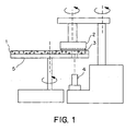
- FIG. 1 depicts a chemical-mechanical polishing (CMP) apparatus in accordance with one embodiment of the invention.
- CMP chemical-mechanical polishing
- the invention is directed to a chemical-mechanical polishing pad substrate comprising a porous material, wherein the polishing pad substrate has at least a certain degree of transparency.
- the polishing pad substrate can be a portion within a polishing pad, or the polishing pad substrate can be an entire polishing pad (e.g., the entire polishing pad or polishing top pad is transparent).
- the polishing pad substrate consists of, or consists essentially of, the porous material.
- the polishing pad substrate comprises a volume of the polishing pad that is at least 0.5 cm 3 (e.g., at least 1 cm 3 ).
- the porous material of the polishing pad substrate has an average pore size of 0.01 microns to 1 micron.
- the average pore size is 0.05 microns to 0.9 microns (e.g., 0.1 microns to 0.8 microns). While not wishing to be bound to any particular theory, it is believed that pore sizes greater than 1 micron will scatter incident radiation, while pore size less than 1 micron will scatter less incident radiation, or will not scatter the incident radiation at all, thereby providing the polishing pad substrate with a desirable degree of transparency.
- the porous material of the polishing pad substrate has a highly uniform distribution of pore sizes (i.e., cell sizes).
- pore sizes i.e., cell sizes
- 75% or more (e.g., 80% or more, or 85% or more) of the pores (e.g., cells) in the porous material have a pore size distribution of ⁇ 0.5 ⁇ m or less (e.g., ⁇ 0.3 ⁇ m or less, or ⁇ 0.2 ⁇ m or less).
- 75% or more (e.g., 80% or more, or 85% or more) of the pores in the porous material have a pore size within 0.5 ⁇ m or less (e.g., 0.3 ⁇ m or less, or 0.2 ⁇ m or less) of the average pore size.
- 90% or more (e.g., 93% or more, or 95% or more) of the pores (e.g., cells) in the porous material have a pore size distribution of ⁇ 0.5 ⁇ m or less (e.g., ⁇ 0.3 ⁇ m or less, or ⁇ 0.2 ⁇ m or less).
- the porous material of the polishing pad substrate comprises predominantly closed cells (i.e., pores); however, the porous material can also comprise open cells.
- the porous material comprises at least 10% or more (e.g., at least 20% or more) closed cells. More preferably, the porous material comprises at least 30% or more (e.g., at least 50% or more, or at least 70% or more) closed cells.
- the porous material of the polishing pad substrate can have any suitable density
- the porous material has a density of 0.2 g/cm 3 or greater (e.g., 0.3 g/cm 3 or greater, or even 0.4 g/cm 3 or greater), preferably a density of 0.5 g/cm 3 or greater (e.g., 0.7 g/cm 3 or greater, or even 0.9 g/cm 3 or greater).
- the void volume is 75% or less, (e.g. 50% or less), preferably 25% or less (e.g., 15% or less, 10% or less, or even 5% or less).
- the porous material has a cell density of 10 5 cells/cm 3 or greater (e.g., 10 6 cells/cm 3 or greater).
- the cell density is determined by analyzing a cross-sectional image (e.g., an SEM image) of a porous material with an image analysis software program such as Optimas® imaging software and ImagePro® imaging software, both by Media Cybernetics, or Clemex Vision® imaging software by Clemex Technologies.
- the porous material of the polishing pad substrate can comprise any suitable material and typically comprises a polymer resin.
- the porous material preferably comprises a polymer resin selected from the group consisting of thermoplastic elastomers, thermoplastic polyurethanes, polyolefins, polycarbonates, polyvinylalcohols, nylons, elastomeric rubbers, styrenic polymers, polyaromatics, fluoropolymers, polyimides, cross-linked polyurethanes, cross-linked polyolefins, polyethers, polyesters, polyacrylates, elastomeric polyethylenes, polytetrafluoroethylene, polyethyleneteraphthalate, polyimides, polyaramides, polyarylenes, polystyrenes, polymethylmethacrylates, copolymers and block copolymers thereof, and mixtures and blends thereof.
- the polymer resin is thermoplastic polyurethane.
- the polymer resin typically is a pre-formed polymer resin; however, the polymer resin also can be formed in situ according to any suitable method, many of which are known in the art (see, for example, Szycher's Handbook of Polyurethanes, CRC Press: New York, 1999, Chapter 3).
- thermoplastic polyurethane can be formed in situ by reaction of urethane prepolymers, such as isocyanate, di-isocyanate, and tri-isocyanate prepolymers, with a prepolymer containing an isocyanate reactive moiety.
- Suitable isocyanate reactive moieties include amines and polyols.
- the selection of the polymer resin will depend, in part, on the rheology of the polymer resin.
- Rheology is the flow behavior of a polymer melt.
- the viscosity is a constant defined by the ratio between the shear stress (i.e., tangential stress, ⁇ ) and the shear rate (i.e., velocity gradient, d ⁇ /dt).
- shear rate thickening i.e., tangential stress, ⁇
- shear rate thinning pseudo-plastic
- the viscosity decreases with increasing shear rate.
- the rheology of the polymer resins must be determined.
- the rheology can be determined by a capillary technique in which the molten polymer resin is forced under a fixed pressure through a capillary of a particular length. By plotting the apparent shear rate versus viscosity at different temperatures, the relationship between the viscosity and temperature can be determined.
- the Rheology Processing Index (RPI) is a parameter that identifies the critical range of the polymer resin.
- the RPI is the ratio of the viscosity at a reference temperature to the viscosity after a change in temperature equal to 20°C for a fixed shear rate.
- the RPI preferably is 2 to 10 (e.g., 3 to 8) when measured at a shear rate of 1501/s and a temperature of 205°C.
- MFI Melt Flow Index
- the MFI preferably is 5 or less (e.g., 4 or less) over 10 minutes at a temperature of 210°C and a load of 2160 g.
- the MFI preferably is 8 or less (e.g., 5 or less) over 10 minutes at a temperature of 210°C and a load of 2160 g.
- the rheology of the polymer resin can depend on the molecular weight, polydispersity index (PDI), the degree of long-chain branching or cross-linking, glass transition temperature (T g ), and melt temperature (T m ) of the polymer resin.
- PDI polydispersity index
- T g glass transition temperature
- T m melt temperature of the polymer resin.
- M w weight average molecular weight
- M w weight average molecular weight
- M w is typically 50,000 g/mol to 300,000 g/mol, preferably 70,000 g/mol to 150,000 g/mol, with a PDI of 1.1 to 6, preferably 2 to 4.
- the thermoplastic polyurethane has a glass transition temperature of 20°C to 110°C and a melt transition temperature of 120°C to 250°C.
- the polymer resin is an elastomeric polyolefin or a polyolefin copolymer (such as the copolymers described above)
- the weight average molecular weight (M w ) typically is 50,000 g/mol to 400,000 g/mol, preferably 70,000 g/mol to 300,000 g/mol, with a PDI of 1.1 to 12, preferably 2 to 10.
- the weight average molecular weight (M w ) typically is 50,000 g/mol to 150,000 g/mol, preferably 70,000 g/mol to 100,000 g/mol, with a PDI of 1.1 to 5, preferably 2 to 4.
- the polymer resin selected for the porous material preferably has certain mechanical properties.
- the Flexural Modulus (ASTM D790) preferably is 350 MPa ( ⁇ 50,000 psi) to 1000 MPa ( ⁇ 150,000 psi), the average % compressibility is 7 or less, the average % rebound is 35 or greater, and the Shore D hardness (ASTM D2240-95) is 40 to 90 (e.g., 50 to 80).
- the polishing pad substrate has a light transmittance of 10% or more (e.g., 20% or more) at at least one wavelength in the range of 200 nm to 35,000 nm.
- the porous material has a light transmittance of 30% or more (e.g., 40% or more, or even 50% or more) at at least one wavelength in the range of 200 nm to 35,000 nm (e.g., 200 nm to 10,000 nm, or 200 nm to 1,000 nm, or even 200 nm to 800 nm).
- the light transmittance of the polishing pad substrate is at least in part determined by controlling properties of the porous material selected from the group consisting of density, void volume, Flexural Modulus, and combinations thereof.
- the polishing pad substrate of the invention offers improved consistency of the light transmittance over the lifetime of the polishing pad substrate. This feature arises from the fact that the pores are present throughout the thickness of the polishing pad substrate. Thus, when the surface layer is removed during polishing, the subsequent layers beneath the surface have substantially similar porosity and roughness, and thus have substantially similar polishing properties and light transmittance properties to the top surface layer. In addition, the transmissivity of the polishing pad substrate is on average lower than the same material without pores because of the roughness, and so the percentage change in light scattering due to any change resulting from abrasion of the polishing pad substrate during polishing is also lessened.
- the light transmittance of the polishing pad substrate decreases by less than 20% (e.g., less than 10%, or even less than 5%) over the lifetime of the polishing pad substrate.
- the consistency in light transmittance of the polishing pad substrate of the invention can be compared to a solid, or nearly solid, polyurethane window of the prior art.
- solid polyurethane windows have consistent surface properties; however, during polishing the window becomes abraded and scratched giving rise to inconsistent surface properties. Therefore, an endpoint detection system must be constantly adjusted in response to each new pattern of scratches that arises during polishing.
- the polishing pad substrate of the invention begins with a roughened surface that remains substantially unchanged during and after abrasion during polishing such that the endpoint detection settings can remain substantially unchanged over the lifetime of the polishing pad substrate.
- the presence of pores in the polishing pad substrate of the invention can have a significant effect on the polishing properties.
- the pores are capable of absorbing and transporting polishing slurry.
- the transmissive region can have polishing properties that are more similar to the remaining portions of the polishing pad.
- the surface texture of the transmissive polishing pad substrate is sufficient to make the polishing pad substrate useful as a polishing surface without the need for a second, opaque portion of the polishing pad that is used exclusively for polishing.
- the polishing pad substrate of the invention optionally further comprises a dye, which enables the substrate to selectively transmit light of a particular wavelength(s).
- the dye acts to filter out undesired wavelengths of light (e.g., background light) and thus improve the signal to noise ratio of detection.
- the polishing pad substrate can comprise any suitable dye or may comprise a combination of dyes. Suitable dyes include polymethine dyes, di-and tri-arylmethine dyes, aza analogues of diarylmethine dyes, aza (18) annulene dyes, natural dyes, nitro dyes, nitroso dyes, azo dyes, anthraquinone dyes, sulfur dyes, and the like.
- the transmission spectrum of the dye matches or overlaps with the wavelength of light used for in situ endpoint detection.
- the dye preferably is a red dye.
- the polishing pad substrate of the invention can be produced using any suitable technique, many of which are known in the art.
- the polishing pad substrate can be produced by (a) a mucell process, (b) a sol-gel process, (c) a phase inversion process, (d) a spinodal or bimodal decomposition process, or (e) a pressurized gas injection process.
- the mucell process involves (a) combining a polymer resin with a supercritical gas to produce a single-phase solution and (b) forming a polishing pad substrate of the invention from the single-phase solution.
- the polymer resin can be any of the polymer resins described above.
- a supercritical gas is generated by subjecting a gas to an elevated temperature (e.g., 100°C to 300°C) and pressure (e.g., 5 MPa ( ⁇ 800 psi) to 40 MPa ( ⁇ 6000 psi)) sufficient to create a supercritical state in which the gas behaves like a fluid (i.e., a supercritical fluid, SCF).
- the gas can be a hydrocarbon, chlorofluorocarbon, hydrochlorofluorocarbon (e.g., freon), nitrogen, carbon dioxide, carbon monoxide, or a combination thereof.
- the gas is a non-flammable gas, for example a gas that does not contain C-H bonds.
- the single-phase solution of the polymer resin and the supercritical gas typically is prepared by blending the supercritical gas with molten polymer resin in a machine barrel. The single-phase solution then can be injected into a mold, where the gas expands to form a pore structure with high uniformity of pore size within the molten polymer resin.
- the concentration of the supercritical gas in the single-phase solution typically is 0.01% to 5% (e.g., 0.1% to 3%) of the total volume of the single-phase solution.
- the thermodynamic instability is induced at the exit of the mold or die which contains the single-phase solution.
- the porous material can be formed from the single-phase solution by any suitable technique including extrusion into a polymer sheet, co-extrusion of multilayer sheets, injection molding, compression molding, blow molding, blown film, multilayer blown film, cast film, thermoforming, and lamination.
- the polishing pad substrate e.g., the porous material
- the pore size of the porous material is at least in part controlled by the temperature, pressure, and concentration of the supercritical gas, and combinations thereof.
- the sol-gel process involves the preparation of a three-dimensional metal oxide network (e.g., siloxane network) having a controllable pore size, surface area, and pore size distribution.
- a three-dimensional metal oxide network e.g., siloxane network
- sol-gels can be prepared using a variety of methods, many of which are known in the art. Suitable methods include single-step (e.g., "one-pot") methods and two-step methods. In one method, a dilute, aqueous solution of silica (e.g., sodium silicate) is prepared which spontaneously condenses under appropriate pH and salt concentration conditions, to form the silicon-based network.
- silica e.g., sodium silicate
- M(OR) 4 metal alkoxide precursors
- R is an alkyl, aryl, or a combination thereof
- M-O-M linkages e.g., Si-O-Si siloxane linkages
- catalysts such as protic acids (e.g., HCl) and bases (e.g., ammonia) can be used to improve the kinetics of the hydrolysis and condensation reactions.
- Two-step methods typically involve the use of pre-polymerized precursors such as pre-polymerized tetraethyl orthosilicate (TEOS).
- TEOS tetraethyl orthosilicate
- a three-dimensional network is formed which contains pores that are filled with solvent (e.g., water).
- solvent e.g., water
- the solvent can be exchanged with alcohol to form a structure referred to as an alcogel.
- Simple evaporation of the solvent typically leads to considerable destruction of the solid three-dimensional network resulting in the formation of a xerogel.
- a more preferred drying technique, which does not result in substantial destruction of the solid three-dimensional network, is supercritical extraction.
- Supercritical extraction typically involves combining the solid three-dimensional network with a suitable low molecular weight expanding agent (such as an alcohol, in particular methanol, as is present in an alcogel, or CO 2 gas which is accomplished by gas/solvent exchange) and applying a temperature and pressure to the mixture that is above the critical point of the expanding agent. Under these conditions, vitrification, cross-linking, or polymerization of the solid material can occur. The pressure is then slowly lowered to allow the expanding agent to diffuse out of the vitrified structure.
- the resulting sol-gel material referred to as an aerogel, has a microcellular pore structure in which the average pore size and pore size distribution can be controlled.
- Such aerogel materials can be transparent to visible or ultraviolet light having a wavelength above 250 nm.
- Hybrid organic-inorganic sol-gel materials also can be transparent, or at least partially transparent.
- Hybrid sol-gel materials typically are prepared using chemical precursors containing both inorganic and organic groups. When a three-dimensional M-O-M network is formed from such precursors, the organic groups can become trapped inside the pore structure. The pore size can be controlled through the selection of an appropriate organic group.
- Examples of hybrid sol-gel materials include clay-polyamide hybrid materials and metal oxide-polymer hybrid materials.
- the phase inversion process involves the dispersion of extremely fine particles of a polymer resin that have been heated above the T m or T g of the polymer in a highly agitated non-solvent.
- the polymer resin can be any of the polymer resins described above.
- the non-solvent can be any suitable solvent having a high Flory-Higgins polymer-solvent interaction parameter (e.g., a Flory-Higgins interaction parameter greater than 0.5).
- Flory-Higgins polymer-solvent interaction parameter e.g., a Flory-Higgins interaction parameter greater than 0.5.
- the polymer resin is a thermoplastic polyurethane
- an aromatic ether-based polyurethane strongly polar solvents such as ethers, ketones, chloroform, dimethylformamide, and the like have interaction parameters less than 0.3 and will act as "good solvents" for the polymer.
- hydrocarbon solvents such as cyclohexane, cyclobutane, and n-alkanes have an interaction parameter greater than 0.5 and function as poor solvents or "non-solvents.”
- the Flory-Higgins interaction parameter is sensitive to temperature so a solvent that is a good solvent at high temperatures may become a non-solvent at lower temperatures.
- the non-solvent mixture is then cooled causing the non-solvent to form into discrete droplets within the three-dimensional polymer network.
- the resulting material is a polymer material having sub-micron pore sizes.
- the spinodal or binodal decomposition process involves controlling the temperature and/or volume fraction of a polymer-polymer mixture, or a polymer-solvent mixture, so as to move the mixture from a single-phase region into a two-phase region. Within the two-phase region, either spinodal decomposition or binodal decomposition of the polymer mixture can occur.
- Decomposition refers to the process by which a polymer-polymer mixture changes from a nonequilibrium phase to an equilibrium phase. In the spinodal region, the free energy of mixing curve is negative such that phase separation of the polymers (i.e., formation of a two-phase material), or phase separation of the polymer and the solvent, is spontaneous in response to small fluctuations in the volume fraction.
- the polymer mixture In the binodal region, the polymer mixture is stable with respect to small fluctuations in volume fraction and thus requires nucleation and growth to achieve a phase-separated material. Precipitation of the polymer mixture at a temperature and volume fraction within the two-phase region (i.e., the binodal or spinodal region) results in the formation of a polymer material having two phases. If the polymer mixture is laden with a solvent or a gas, the biphasic polymer material will contain sub-micron pores at the interface of the phase-separation.
- the polymers preferably comprise the polymer resins described above.
- the pressurized gas injection process involves the use of high temperatures and pressures to force a supercritical fluid gas into a solid polymer sheet comprising a polymer resin.
- the polymer resin can be any of the polymer resins described above.
- Solid extruded sheets are placed at room temperature into a pressure vessel.
- a supercritical gas e.g., N 2 or CO 2 is added to the vessel, and the vessel is pressurized to a level sufficient to force an appropriate amount of the gas into the free volume of the polymer sheet.
- the amount of gas dissolved in the polymer is directly proportional to the applied pressure according to Henry's law. Increasing the temperature of the polymer sheet increases the rate of diffusion of the gas into the polymer, but also decreases the amount of gas that can dissolve in the polymer sheet.
- the sheet is removed from the pressurized vessel.
- the resulting polymer sheet typically has cell sizes ranging from 0.5 microns to 1 micron. If desired, the polymer sheet can be quickly heated to a softened or molten state.
- the pore size of the porous material is at least in part controlled by the temperature, pressure, and concentration of the supercritical gas, and combinations thereof.
- the polishing pad substrate of the invention can be mounted into a polishing pad using any suitable technique.
- the polishing pad substrate can be mounted into a polishing pad through the use of adhesives.
- the polishing pad substrate can be mounted into the top portion of the polishing pad (e.g., the polishing surface), or can be mounted into the bottom portion of the polishing pad (e.g., the subpad).
- the polishing pad substrate can have any suitable dimensions and can be round, oval, square, rectangular, triangular, and so on.
- the polishing pad substrate can be positioned so as to be flush with the polishing surface of the polishing pad, or can be recessed from the polishing surface of the polishing pad.
- the polishing pad can comprise one or more of the polishing pad substrates of the invention.
- the polishing pad substrate(s) can be placed in any suitable position on the polishing pad relative to the center and/or periphery of the polishing pad.
- the polishing pad into which the polishing pad substrate is placed can be made of any suitable polishing pad material, many of which are known in the art.
- the polishing pad typically is opaque or only partially translucent.
- the polishing pad can comprise any suitable polymer resin.
- the polishing pad typically comprises a polymer resin selected from the group consisting of thermoplastic elastomers, thermoplastic polyurethanes, thermoplastic polyolefins, polycarbonates, polyvinylalcohols, nylons, elastomeric rubbers, elastomeric polyethylenes, polytetrafluoroethylene, polyethyleneteraphthalate, polyimides, polyaramides, polyarylenes, polystyrenes, polymethylmethacrylates, copolymers thereof, and mixtures thereof.
- the polishing pad can be produced by any suitable method including sintering, injection molding, blow molding, extrusion, and the like.
- the polishing pad can be solid and non-porous, can contain microporous closed cells, can contain open cells, or can contain a fibrous web onto which a polymer has been molded.
- Polishing pads comprising the polishing pad substrate of the invention have a polishing surface which optionally further comprises grooves, channels, and/or perforations which facilitate the lateral transport of polishing compositions across the surface of the polishing pad.
- Such grooves, channels, or perforations can be in any suitable pattern and can have any suitable depth and width.
- the polishing pad can have two or more different groove patterns, for example a combination of large grooves and small grooves as described in U.S. Patent 5,489,233 .
- the grooves can be in the form of slanted grooves, concentric grooves, spiral or circular grooves, XY crosshatch pattern, and can be continuous or non-continuous in connectivity.
- the polishing pad comprises at least small grooves produced by standard pad conditioning methods.
- Polishing pads comprising the polishing pad substrate of the invention can comprise, in addition to the polishing pad substrate, one or more other features or components.
- the polishing pad optionally can comprise regions of differing density, hardness, porosity, and chemical compositions.
- the polishing pad optionally can comprise solid particles including abrasive particles (e.g., metal oxide particles), polymer particles, water-soluble particles, water-absorbent particles, hollow particles, and the like.
- Polishing pads comprising the polishing pad substrate of the invention are particularly suited for use in conjunction with a chemical-mechanical polishing (CMP) apparatus.
- the apparatus comprises a platen 5, which, when in use, is in motion and has a velocity that results from orbital, linear, or circular motion, a polishing pad 1 comprising the polishing pad substrate of the invention in contact with platen 5 and moving with the platen when in motion, and a carrier 2 that holds a workpiece 3 to be polished by contacting and moving relative to the surface of polishing pad 1.
- CMP chemical-mechanical polishing
- the polishing of the workpiece takes place by the workpiece being placed in contact with the polishing pad and then the polishing pad moving relative to the workpiece, typically with a polishing composition therebetween, so as to abrade at least a portion of the workpiece to polish the workpiece.
- the polishing composition typically comprises a liquid carrier (e.g., an aqueous carrier), a pH adjustor, and optionally an abrasive.
- the polishing composition optionally may further comprise oxidizing agents, organic acids, complexing agents, pH buffers, surfactants, corrosion inhibitors, antifoaming agents, and the like.
- the CMP apparatus can be any suitable CMP apparatus, many of which are known in the art.
- the polishing pad comprising the polishing pad substrate of the invention also can be used with linear polishing tools.
- the CMP apparatus further comprises an in situ polishing endpoint detection system 4, many of which are known in the art.
- Techniques for inspecting and monitoring the polishing process by analyzing light or other radiation reflected from a surface of the workpiece are known in the art. Such methods are described, for example, in U.S. Patent 5,196,353 , U.S. Patent 5,433,651 , U.S. Patent 5,609,511 , U.S. Patent 5,643,046 , U.S. Patent 5,658,183 , U.S. Patent 5,730,642 , U.S. Patent 5,838,447 , U.S. Patent 5,872,633 , U.S. Patent 5,893,796 , U.S.
- Patent 5,949,927 and U.S. Patent 5,964,643 .
- the inspection or monitoring of the progress of the polishing process with respect to a workpiece being polished enables the determination of the polishing end-point, i.e., the determination of when to terminate the polishing process with respect to a particular workpiece.
- a polishing pad comprising the polishing pad substrate of the invention can be used alone or optionally can be used as one layer of a multi-layer stacked polishing pad.
- the polishing pad can be used in combination with a subpad.
- the subpad can be any suitable subpad. Suitable subpads include polyurethane foam subpads (e.g., Poron® foam subpads from Rogers Corporation), impregnated felt subpads, microporous polyurethane subpads, or sintered urethane subpads.
- the subpad typically is softer than the polishing pad comprising the polishing pad substrate of the invention and therefore is more compressible and has a lower Shore hardness value than the polishing pad.
- the subpad can have a Shore A hardness of 35 to 50. In some embodiments, the subpad is harder, is less compressible, and has a higher Shore hardness than the polishing pad.
- the subpad optionally comprises grooves, channels, hollow sections, windows, apertures, and the like.
- an intermediate backing layer such as a polyethyleneterephthalate film, coextensive with and between the polishing pad and the subpad.
- Polishing pads comprising the polishing pad substrates of the invention are suitable for use in polishing many types of workpieces (e.g., substrates or wafers) and workpiece materials.
- the polishing pads can be used to polish workpieces including memory storage devices, semiconductor substrates, and glass substrates.
- Suitable workpieces for polishing with the polishing pads include memory or rigid disks, magnetic heads, MEMS devices, semiconductor wafers, field emission displays, and other microelectronic substrates, especially microelectronic substrates comprising insulating layers (e.g., silicon dioxide, silicon nitride, or low dielectric materials) and/or metal-containing layers (e.g., copper, tantalum, tungsten, aluminum, nickel, titanium, platinum, ruthenium, rhodium, iridium or other noble metals).
- insulating layers e.g., silicon dioxide, silicon nitride, or low dielectric materials
- metal-containing layers e.g., copper, tantalum, tungsten, aluminum, nickel, titanium, platinum, ruthenium, rhodium, iridium or other noble metals.
Landscapes
- Engineering & Computer Science (AREA)
- Mechanical Engineering (AREA)
- Physics & Mathematics (AREA)
- Condensed Matter Physics & Semiconductors (AREA)
- General Physics & Mathematics (AREA)
- Manufacturing & Machinery (AREA)
- Computer Hardware Design (AREA)
- Microelectronics & Electronic Packaging (AREA)
- Power Engineering (AREA)
- Mechanical Treatment Of Semiconductor (AREA)
- Finish Polishing, Edge Sharpening, And Grinding By Specific Grinding Devices (AREA)
- Manufacture Of Porous Articles, And Recovery And Treatment Of Waste Products (AREA)
Claims (15)
- Chemisch-mechanisches Polierkissensubstrat, welches einen feinporigen Werkstoff umfasst, wobei das Polierkissensubstrat eine Lichtdurchlässigkeit von 10% oder mehr bei einer Wellenlänge von mindestens 200 nm bis 35.000 nm aufweist,
dadurch gekennzeichnet, dass
der feinporige Werkstoff eine durchschnittliche Porengröße von 0,01 Mikron bis 1 Mikron und ein Hohlraumvolumen von 75% oder weniger aufweist. - Polierkissensubstrat nach Anspruch 1,
dadurch gekennzeichnet, dass
das Polierkissensubstrat eine Lichtdurchlässigkeit von 30% oder mehr bei einer Wellenlänge von mindestens 200 nm bis 35.000 nm aufweist. - Polierkissensubstrat nach Anspruch 1,
dadurch gekennzeichnet, dass
die durchschnittliche Porengröße 0,1 Mikron bis 0,7 Mikron beträgt. - Polierkissensubstrat nach Anspruch 1,
dadurch gekennzeichnet, dass
der feinporige Werkstoff eine Dichte von 0,5 g/cm3 oder größer aufweist. - Polierkissensubstrat nach Anspruch 4,
dadurch gekennzeichnet, dass
der feinporige Werkstoff eine Dichte von 0,7 g/cm3 oder größer aufweist. - Polierkissensubstrat nach Anspruch 1,
dadurch gekennzeichnet, dass
der feinporige Werkstoff ein Hohlraumvolumen von 50% oder weniger aufweist. - Polierkissensubstrat nach Anspruch 6,
dadurch gekennzeichnet, dass
der feinporige Werkstoff ein Hohlraumvolumen von 25% oder weniger aufweist. - Polierkissensubstrat nach Anspruch 1,
dadurch gekennzeichnet, dass
der feinporige Werkstoff ein aus der aus thermoplastischen Elastomeren, thermoplastischen Polyurethanen, thermoplastischen Polyolefinen, Polykarbonaten, Polyvinylalkoholen, Nylons, Elastomergummis, Elastomerpolyethylenen, Polytetrafluorethylen, Polyethylenteraphthalat, Polyimiden, Polyaramiden, Polyarylenen, Polystyrolen, Polymethylmethakrylaten, Copolymeren davon und Mischungen davon bestehenden Gruppe ausgewähltes Polymerharz umfasst. - Polierkissensubstrat nach Anspruch 8,
dadurch gekennzeichnet, dass
das Polymerharz ein thermoplastisches Polyurethan ist. - Polierkissensubstrat nach Anspruch 1,
dadurch gekennzeichnet, dass
der feinporige Werkstoff ein dreidimensionales Metalloxidnetzwerk umfasst. - Polierkissensubstrat nach Anspruch 1,
dadurch gekennzeichnet, dass
das Substrat ein Polierkissen ist. - Polierkissensubstrat nach Anspruch 1,
dadurch gekennzeichnet, dass
das Substrat ein Polierkissenfenster ist. - Chemisch-mechanische Poliervorrichtung, die Folgendes umfasst:(a) eine sich drehende Platte (5),(b) ein Polierkissen (1) und(c) einen Träger (2), der ein zu polierendes Werkstück (3) hält, indem er ein sich drehendes Polierkissen berührt, wobei das Polierkissen das Polierkissensubstrat nach Anspruch 1 umfasst.
- Chemisch-mechanische Poliervorrichtung nach Anspruch 13,
dadurch gekennzeichnet, dass
es weiterhin ein lokales Polierendpunkterkennungssystem (4) umfasst. - Verfahren zum Polieren eines Werkstückes, welches Folgendes umfasst:(a) Bereitstellung eines Polierkissens (1),(b) Berühren eines Werkstückes (3) mit dem Polierkissen und(c) Bewegen des Polierkissens im Verhältnis zu dem Werkstück, um das Werkstück abzuschleifen und das Werkstück dadurch zu polieren, wobei das Polierkissen das Polierkissensubstrat nach Anspruch 1 umfasst.
Applications Claiming Priority (3)
| Application Number | Priority Date | Filing Date | Title |
|---|---|---|---|
| US282489 | 1994-08-01 | ||
| US10/282,489 US7435165B2 (en) | 2002-10-28 | 2002-10-28 | Transparent microporous materials for CMP |
| PCT/IB2003/004476 WO2004037490A1 (en) | 2002-10-28 | 2003-10-06 | Transparent microporous materials for cmp |
Publications (2)
| Publication Number | Publication Date |
|---|---|
| EP1567306A1 EP1567306A1 (de) | 2005-08-31 |
| EP1567306B1 true EP1567306B1 (de) | 2007-07-04 |
Family
ID=32107376
Family Applications (1)
| Application Number | Title | Priority Date | Filing Date |
|---|---|---|---|
| EP03809403A Expired - Lifetime EP1567306B1 (de) | 2002-10-28 | 2003-10-06 | Transparente mikroporöse materialien für cmp |
Country Status (10)
| Country | Link |
|---|---|
| US (1) | US7435165B2 (de) |
| EP (1) | EP1567306B1 (de) |
| JP (4) | JP2006504260A (de) |
| KR (1) | KR101065117B1 (de) |
| CN (1) | CN100589934C (de) |
| AT (1) | ATE366165T1 (de) |
| AU (1) | AU2003264819A1 (de) |
| DE (1) | DE60314772T2 (de) |
| TW (1) | TWI234505B (de) |
| WO (1) | WO2004037490A1 (de) |
Families Citing this family (56)
| Publication number | Priority date | Publication date | Assignee | Title |
|---|---|---|---|---|
| TW591089B (en) | 2001-08-09 | 2004-06-11 | Cheil Ind Inc | Slurry composition for use in chemical mechanical polishing of metal wiring |
| US6953389B2 (en) * | 2001-08-09 | 2005-10-11 | Cheil Industries, Inc. | Metal CMP slurry compositions that favor mechanical removal of oxides with reduced susceptibility to micro-scratching |
| US7267607B2 (en) * | 2002-10-28 | 2007-09-11 | Cabot Microelectronics Corporation | Transparent microporous materials for CMP |
| US7311862B2 (en) * | 2002-10-28 | 2007-12-25 | Cabot Microelectronics Corporation | Method for manufacturing microporous CMP materials having controlled pore size |
| US6984163B2 (en) * | 2003-11-25 | 2006-01-10 | Rohm And Haas Electronic Materials Cmp Holdings, Inc. | Polishing pad with high optical transmission window |
| TWI293266B (en) * | 2004-05-05 | 2008-02-11 | Iv Technologies Co Ltd | A single-layer polishing pad and a method of producing the same |
| JP4845347B2 (ja) * | 2004-05-17 | 2011-12-28 | 東洋ゴム工業株式会社 | 研磨パッドおよびその製造方法 |
| KR100699522B1 (ko) * | 2005-06-30 | 2007-03-27 | (주)제이티앤씨 | 웨이퍼용 연마패드의 제조방법 및 그 연마패드 |
| TWI378844B (en) * | 2005-08-18 | 2012-12-11 | Rohm & Haas Elect Mat | Polishing pad and method of manufacture |
| TW200709892A (en) * | 2005-08-18 | 2007-03-16 | Rohm & Haas Elect Mat | Transparent polishing pad |
| JP5110677B2 (ja) * | 2006-05-17 | 2012-12-26 | 東洋ゴム工業株式会社 | 研磨パッド |
| JP2007307639A (ja) * | 2006-05-17 | 2007-11-29 | Toyo Tire & Rubber Co Ltd | 研磨パッド |
| US7838108B2 (en) * | 2007-01-17 | 2010-11-23 | Sabic Innovative Plastics Ip B.V. | Nano-cellular polymer foam and methods for making them |
| EP2711156A3 (de) * | 2007-03-12 | 2014-09-17 | University of Washington | Schäumungsverfahren zur Herstellung von thermoplastischem zellulärem Material |
| US7842379B2 (en) * | 2007-07-05 | 2010-11-30 | Sabic Innovative Plastics Ip B.V. | Polymeric foams with nanocellular morphology and methods for making them |
| KR101431512B1 (ko) * | 2007-08-27 | 2014-08-20 | 주식회사 동진쎄미켐 | 초임계 유체를 이용한 금속층의 기계화학적 연마방법 및장치 |
| WO2009070352A1 (en) * | 2007-11-30 | 2009-06-04 | Innopad, Inc. | Chemical-mechanical planarization pad having end point detection window |
| US8908129B2 (en) * | 2007-12-28 | 2014-12-09 | Sabic Global Technologies B.V. | Reflective polymeric article and manufacture |
| JP2011507720A (ja) * | 2007-12-31 | 2011-03-10 | イノパッド,インコーポレイテッド | 化学的機械的平坦化パッド |
| US8440732B2 (en) * | 2008-03-25 | 2013-05-14 | Sabic Innovative Plastics Ip B.V. | Polymeric foams with nanocellular morphology and methods for making them |
| KR101618273B1 (ko) * | 2008-04-29 | 2016-05-04 | 세미퀘스트, 인코포레이티드 | 연마 패드 조성물, 및 이의 제조 방법 및 용도 |
| JP5336799B2 (ja) * | 2008-09-24 | 2013-11-06 | 東京エレクトロン株式会社 | 化学的機械研磨装置、化学的機械研磨方法及び制御プログラム |
| JP5748747B2 (ja) * | 2009-06-10 | 2015-07-15 | エルジー・ケム・リミテッド | 多孔性シートの製造方法及びこれにより製造された多孔性シート |
| US8283390B2 (en) * | 2009-09-10 | 2012-10-09 | Sabic Innovative Plastics Ip B.V. | Siloxane block copolymer nanoporous foams, methods of manufacture thereof and articles comprising the same |
| US8162728B2 (en) * | 2009-09-28 | 2012-04-24 | Rohm And Haas Electronic Materials Cmp Holdings, Inc. | Dual-pore structure polishing pad |
| US9017140B2 (en) | 2010-01-13 | 2015-04-28 | Nexplanar Corporation | CMP pad with local area transparency |
| US8697217B2 (en) * | 2010-01-15 | 2014-04-15 | Rohm and Haas Electronics Materials CMP Holdings, Inc. | Creep-resistant polishing pad window |
| RU2012143158A (ru) | 2010-03-10 | 2014-04-20 | ДАУ ГЛОБАЛ ТЕКНОЛОДЖИЗ ЭлЭлСи | Нанопористый пенополимер, характеризующийся высокой алотностью ячеек в отсутствие нанонаполнителя |
| US9156124B2 (en) | 2010-07-08 | 2015-10-13 | Nexplanar Corporation | Soft polishing pad for polishing a semiconductor substrate |
| US8758659B2 (en) | 2010-09-29 | 2014-06-24 | Fns Tech Co., Ltd. | Method of grooving a chemical-mechanical planarization pad |
| US9156125B2 (en) | 2012-04-11 | 2015-10-13 | Cabot Microelectronics Corporation | Polishing pad with light-stable light-transmitting region |
| DE202014007186U1 (de) * | 2014-09-09 | 2015-08-27 | Kolthoff Gabrovo Eood | Werkzeug zur Oberflächenfeinbearbeitung |
| US9873180B2 (en) | 2014-10-17 | 2018-01-23 | Applied Materials, Inc. | CMP pad construction with composite material properties using additive manufacturing processes |
| US10875153B2 (en) | 2014-10-17 | 2020-12-29 | Applied Materials, Inc. | Advanced polishing pad materials and formulations |
| US10875145B2 (en) | 2014-10-17 | 2020-12-29 | Applied Materials, Inc. | Polishing pads produced by an additive manufacturing process |
| US10821573B2 (en) | 2014-10-17 | 2020-11-03 | Applied Materials, Inc. | Polishing pads produced by an additive manufacturing process |
| US10399201B2 (en) | 2014-10-17 | 2019-09-03 | Applied Materials, Inc. | Advanced polishing pads having compositional gradients by use of an additive manufacturing process |
| US9776361B2 (en) | 2014-10-17 | 2017-10-03 | Applied Materials, Inc. | Polishing articles and integrated system and methods for manufacturing chemical mechanical polishing articles |
| KR102436416B1 (ko) | 2014-10-17 | 2022-08-26 | 어플라이드 머티어리얼스, 인코포레이티드 | 애디티브 제조 프로세스들을 이용한 복합 재료 특성들을 갖는 cmp 패드 구성 |
| US11745302B2 (en) | 2014-10-17 | 2023-09-05 | Applied Materials, Inc. | Methods and precursor formulations for forming advanced polishing pads by use of an additive manufacturing process |
| JP2018524193A (ja) | 2015-07-30 | 2018-08-30 | ジェイエイチ ローデス カンパニー, インコーポレイテッド | ポリマーラップ加工材料、ポリマーラップ加工材料を含む媒体およびシステム、およびそれらを形成し使用する方法 |
| US10618141B2 (en) | 2015-10-30 | 2020-04-14 | Applied Materials, Inc. | Apparatus for forming a polishing article that has a desired zeta potential |
| US10593574B2 (en) | 2015-11-06 | 2020-03-17 | Applied Materials, Inc. | Techniques for combining CMP process tracking data with 3D printed CMP consumables |
| TWI548683B (zh) | 2015-11-10 | 2016-09-11 | 國立臺灣科技大學 | 製造高分子奈米泡材的方法 |
| US10456886B2 (en) | 2016-01-19 | 2019-10-29 | Applied Materials, Inc. | Porous chemical mechanical polishing pads |
| US10391605B2 (en) | 2016-01-19 | 2019-08-27 | Applied Materials, Inc. | Method and apparatus for forming porous advanced polishing pads using an additive manufacturing process |
| US11471999B2 (en) | 2017-07-26 | 2022-10-18 | Applied Materials, Inc. | Integrated abrasive polishing pads and manufacturing methods |
| WO2019032286A1 (en) | 2017-08-07 | 2019-02-14 | Applied Materials, Inc. | ABRASIVE DISTRIBUTION POLISHING PADS AND METHODS OF MAKING SAME |
| WO2020050932A1 (en) | 2018-09-04 | 2020-03-12 | Applied Materials, Inc. | Formulations for advanced polishing pads |
| US11813712B2 (en) | 2019-12-20 | 2023-11-14 | Applied Materials, Inc. | Polishing pads having selectively arranged porosity |
| US11806829B2 (en) | 2020-06-19 | 2023-11-07 | Applied Materials, Inc. | Advanced polishing pads and related polishing pad manufacturing methods |
| KR102848445B1 (ko) | 2020-07-10 | 2025-08-21 | 세인트-고바인 아브라시브즈 인크. | 접합된 연마 물품 및 이의 제조 방법 |
| US11878389B2 (en) | 2021-02-10 | 2024-01-23 | Applied Materials, Inc. | Structures formed using an additive manufacturing process for regenerating surface texture in situ |
| CN113977453B (zh) * | 2021-11-08 | 2023-01-13 | 万华化学集团电子材料有限公司 | 提高抛光平坦度的化学机械抛光垫及其应用 |
| CN115464511B (zh) * | 2022-09-19 | 2023-08-01 | 厦门大学 | 一种集多通道孔径检测及纳米孔制备于一体的装置及其使用方法 |
| CN116749074A (zh) * | 2023-06-27 | 2023-09-15 | 中国地质大学(北京) | 一种改善透光晶圆厚度均匀性的方法及装置 |
Family Cites Families (60)
| Publication number | Priority date | Publication date | Assignee | Title |
|---|---|---|---|---|
| US4138228A (en) | 1977-02-02 | 1979-02-06 | Ralf Hoehn | Abrasive of a microporous polymer matrix with inorganic particles thereon |
| US4239567A (en) | 1978-10-16 | 1980-12-16 | Western Electric Company, Inc. | Removably holding planar articles for polishing operations |
| JPH01193166A (ja) | 1988-01-28 | 1989-08-03 | Showa Denko Kk | 半導体ウェハ鏡面研磨用パッド |
| US5182307A (en) | 1990-11-21 | 1993-01-26 | Board Of Regents Of The University Of Washington | Polyethylene terephthalate foams with integral crystalline skins |
| US5441598A (en) | 1993-12-16 | 1995-08-15 | Motorola, Inc. | Polishing pad for chemical-mechanical polishing of a semiconductor substrate |
| US5489233A (en) | 1994-04-08 | 1996-02-06 | Rodel, Inc. | Polishing pads and methods for their use |
| US5684055A (en) | 1994-12-13 | 1997-11-04 | University Of Washington | Semi-continuous production of solid state polymeric foams |
| US5893796A (en) | 1995-03-28 | 1999-04-13 | Applied Materials, Inc. | Forming a transparent window in a polishing pad for a chemical mechanical polishing apparatus |
| US5964643A (en) | 1995-03-28 | 1999-10-12 | Applied Materials, Inc. | Apparatus and method for in-situ monitoring of chemical mechanical polishing operations |
| US5605760A (en) | 1995-08-21 | 1997-02-25 | Rodel, Inc. | Polishing pads |
| JPH10125634A (ja) * | 1996-10-19 | 1998-05-15 | Nikon Corp | 研磨装置 |
| GB2316414B (en) | 1996-07-31 | 2000-10-11 | Tosoh Corp | Abrasive shaped article, abrasive disc and polishing method |
| WO1998008667A2 (en) | 1996-08-27 | 1998-03-05 | Trexel, Inc. | Method and apparatus for microcellular polymer extrusion |
| JPH10166262A (ja) * | 1996-12-10 | 1998-06-23 | Nikon Corp | 研磨装置 |
| WO1998028108A1 (en) | 1996-12-20 | 1998-07-02 | Unique Technology International Private Limited | Manufacture of porous polishing pad |
| US6022268A (en) | 1998-04-03 | 2000-02-08 | Rodel Holdings Inc. | Polishing pads and methods relating thereto |
| US6287185B1 (en) * | 1997-04-04 | 2001-09-11 | Rodel Holdings Inc. | Polishing pads and methods relating thereto |
| US6126532A (en) * | 1997-04-18 | 2000-10-03 | Cabot Corporation | Polishing pads for a semiconductor substrate |
| KR20010006518A (ko) | 1997-04-18 | 2001-01-26 | 매튜 네빌 | 반도체 기판용 연마 패드 |
| US6146248A (en) * | 1997-05-28 | 2000-11-14 | Lam Research Corporation | Method and apparatus for in-situ end-point detection and optimization of a chemical-mechanical polishing process using a linear polisher |
| US6235380B1 (en) | 1997-07-24 | 2001-05-22 | Trexel, Inc. | Lamination of microcellular articles |
| CA2315234A1 (en) | 1997-12-19 | 1999-07-01 | Trexel, Inc. | Microcellular foam extrusion/blow molding process and article made thereby |
| US6231942B1 (en) | 1998-01-21 | 2001-05-15 | Trexel, Inc. | Method and apparatus for microcellular polypropylene extrusion, and polypropylene articles produced thereby |
| GB2334205B (en) | 1998-02-12 | 2001-11-28 | Shinetsu Handotai Kk | Polishing method for semiconductor wafer and polishing pad used therein |
| US6248000B1 (en) * | 1998-03-24 | 2001-06-19 | Nikon Research Corporation Of America | Polishing pad thinning to optically access a semiconductor wafer surface |
| US6435947B2 (en) * | 1998-05-26 | 2002-08-20 | Cabot Microelectronics Corporation | CMP polishing pad including a solid catalyst |
| US6117000A (en) * | 1998-07-10 | 2000-09-12 | Cabot Corporation | Polishing pad for a semiconductor substrate |
| JP2918883B1 (ja) | 1998-07-15 | 1999-07-12 | 日本ピラー工業株式会社 | 研磨パッド |
| JP3685064B2 (ja) | 1998-08-28 | 2005-08-17 | 東レ株式会社 | 研磨パッド |
| WO2000060650A1 (en) * | 1999-03-31 | 2000-10-12 | Nikon Corporation | Polishing body, polisher, method for adjusting polisher, method for measuring thickness of polished film or end point of polishing, method for producing semiconductor device |
| US6322347B1 (en) | 1999-04-02 | 2001-11-27 | Trexel, Inc. | Methods for manufacturing foam material including systems with pressure restriction element |
| DE60025989T2 (de) | 1999-04-09 | 2006-11-09 | Tosoh Corp., Shinnanyo | Formschleifprodukt und Benutzung in einer Polierscheibe |
| US6656018B1 (en) | 1999-04-13 | 2003-12-02 | Freudenberg Nonwovens Limited Partnership | Polishing pads useful in chemical mechanical polishing of substrates in the presence of a slurry containing abrasive particles |
| JP2000343411A (ja) * | 1999-06-01 | 2000-12-12 | Teijin Ltd | 研磨用シート |
| US6146242A (en) | 1999-06-11 | 2000-11-14 | Strasbaugh, Inc. | Optical view port for chemical mechanical planarization endpoint detection |
| US6171181B1 (en) | 1999-08-17 | 2001-01-09 | Rodel Holdings, Inc. | Molded polishing pad having integral window |
| JP2001062703A (ja) * | 1999-08-27 | 2001-03-13 | Asahi Chem Ind Co Ltd | 多孔性樹脂窓付き研磨パッド |
| US20020090819A1 (en) | 1999-08-31 | 2002-07-11 | Cangshan Xu | Windowless belt and method for improved in-situ wafer monitoring |
| US6602064B1 (en) | 1999-08-31 | 2003-08-05 | Trexel, Inc. | Polymer processing system and apparatus |
| US6358130B1 (en) | 1999-09-29 | 2002-03-19 | Rodel Holdings, Inc. | Polishing pad |
| JP2001105299A (ja) * | 1999-10-01 | 2001-04-17 | Asahi Kasei Corp | 窓付研磨パッド |
| AU2750201A (en) | 1999-11-05 | 2001-05-30 | Trexel, Inc. | Thermoformed polyolefin foams and methods of their production |
| JP2003516872A (ja) * | 1999-12-14 | 2003-05-20 | ロデール ホールディングス インコーポレイテッド | 高分子又は高分子複合材研磨パッドの製造方法 |
| US6368200B1 (en) | 2000-03-02 | 2002-04-09 | Agere Systems Guardian Corporation | Polishing pads from closed-cell elastomer foam |
| JP4634688B2 (ja) | 2000-03-15 | 2011-02-16 | ローム アンド ハース エレクトロニック マテリアルズ シーエムピー ホウルディングス インコーポレイテッド | 調節された摩耗速度を有する窓部 |
| US6454634B1 (en) * | 2000-05-27 | 2002-09-24 | Rodel Holdings Inc. | Polishing pads for chemical mechanical planarization |
| JP3925041B2 (ja) | 2000-05-31 | 2007-06-06 | Jsr株式会社 | 研磨パッド用組成物及びこれを用いた研磨パッド |
| JP2001348271A (ja) * | 2000-06-01 | 2001-12-18 | Tosoh Corp | 研磨用成形体及びこれを用いた研磨用定盤 |
| US6685537B1 (en) | 2000-06-05 | 2004-02-03 | Speedfam-Ipec Corporation | Polishing pad window for a chemical mechanical polishing tool |
| EP1294536B1 (de) | 2000-06-30 | 2005-04-20 | Rohm and Haas Electronic Materials CMP Holdings, Inc. | Unterlage für polierscheibe |
| US6458013B1 (en) | 2000-07-31 | 2002-10-01 | Asml Us, Inc. | Method of chemical mechanical polishing |
| JP2002124491A (ja) * | 2000-08-10 | 2002-04-26 | Toray Ind Inc | 研磨パッド |
| US6641471B1 (en) * | 2000-09-19 | 2003-11-04 | Rodel Holdings, Inc | Polishing pad having an advantageous micro-texture and methods relating thereto |
| CN1468162A (zh) * | 2000-10-06 | 2004-01-14 | 包括填充的半透明区域的抛光垫 | |
| US20020072296A1 (en) | 2000-11-29 | 2002-06-13 | Muilenburg Michael J. | Abrasive article having a window system for polishing wafers, and methods |
| EP1211024A3 (de) | 2000-11-30 | 2004-01-02 | JSR Corporation | Polierverfahren |
| US20020098790A1 (en) | 2001-01-19 | 2002-07-25 | Burke Peter A. | Open structure polishing pad and methods for limiting pore depth |
| US6383065B1 (en) * | 2001-01-22 | 2002-05-07 | Cabot Microelectronics Corporation | Catalytic reactive pad for metal CMP |
| US6840843B2 (en) * | 2001-03-01 | 2005-01-11 | Cabot Microelectronics Corporation | Method for manufacturing a polishing pad having a compressed translucent region |
| JP2002265873A (ja) * | 2001-03-08 | 2002-09-18 | Nihon Micro Coating Co Ltd | 研磨塗料及びその製造方法 |
-
2002
- 2002-10-28 US US10/282,489 patent/US7435165B2/en not_active Expired - Lifetime
-
2003
- 2003-10-06 AU AU2003264819A patent/AU2003264819A1/en not_active Abandoned
- 2003-10-06 WO PCT/IB2003/004476 patent/WO2004037490A1/en not_active Ceased
- 2003-10-06 AT AT03809403T patent/ATE366165T1/de not_active IP Right Cessation
- 2003-10-06 JP JP2004546252A patent/JP2006504260A/ja active Pending
- 2003-10-06 EP EP03809403A patent/EP1567306B1/de not_active Expired - Lifetime
- 2003-10-06 DE DE60314772T patent/DE60314772T2/de not_active Expired - Lifetime
- 2003-10-06 CN CN200380102155A patent/CN100589934C/zh not_active Expired - Fee Related
- 2003-10-06 KR KR1020057007277A patent/KR101065117B1/ko not_active Expired - Fee Related
- 2003-10-09 TW TW092128094A patent/TWI234505B/zh not_active IP Right Cessation
-
2010
- 2010-03-23 JP JP2010066030A patent/JP5675136B2/ja not_active Expired - Fee Related
-
2013
- 2013-06-03 JP JP2013116652A patent/JP5882947B2/ja not_active Expired - Fee Related
-
2015
- 2015-06-19 JP JP2015123439A patent/JP5986268B2/ja not_active Expired - Fee Related
Also Published As
| Publication number | Publication date |
|---|---|
| AU2003264819A1 (en) | 2004-05-13 |
| TWI234505B (en) | 2005-06-21 |
| EP1567306A1 (de) | 2005-08-31 |
| TW200420382A (en) | 2004-10-16 |
| US7435165B2 (en) | 2008-10-14 |
| JP2010166078A (ja) | 2010-07-29 |
| JP2015193077A (ja) | 2015-11-05 |
| KR101065117B1 (ko) | 2011-09-16 |
| DE60314772T2 (de) | 2007-10-31 |
| JP5986268B2 (ja) | 2016-09-06 |
| JP2006504260A (ja) | 2006-02-02 |
| JP5882947B2 (ja) | 2016-03-09 |
| DE60314772D1 (de) | 2007-08-16 |
| JP5675136B2 (ja) | 2015-02-25 |
| ATE366165T1 (de) | 2007-07-15 |
| US20040082276A1 (en) | 2004-04-29 |
| CN1708377A (zh) | 2005-12-14 |
| KR20050061569A (ko) | 2005-06-22 |
| CN100589934C (zh) | 2010-02-17 |
| JP2013201452A (ja) | 2013-10-03 |
| WO2004037490A1 (en) | 2004-05-06 |
Similar Documents
| Publication | Publication Date | Title |
|---|---|---|
| EP1567306B1 (de) | Transparente mikroporöse materialien für cmp | |
| EP1915233B1 (de) | Transparente mikroporöse materialien für cmp | |
| US7311862B2 (en) | Method for manufacturing microporous CMP materials having controlled pore size | |
| KR101109324B1 (ko) | 미세다공성 영역을 갖는 연마 패드 | |
| US6998166B2 (en) | Polishing pad with oriented pore structure | |
| KR20080037719A (ko) | 표면-텍스쳐화 미공질 연마 패드 | |
| WO2004069470A2 (en) | Cmp pad with composite transparent window |
Legal Events
| Date | Code | Title | Description |
|---|---|---|---|
| PUAI | Public reference made under article 153(3) epc to a published international application that has entered the european phase |
Free format text: ORIGINAL CODE: 0009012 |
|
| 17P | Request for examination filed |
Effective date: 20050525 |
|
| AK | Designated contracting states |
Kind code of ref document: A1 Designated state(s): AT BE BG CH CY CZ DE DK EE ES FI FR GB GR HU IE IT LI LU MC NL PT RO SE SI SK TR |
|
| AX | Request for extension of the european patent |
Extension state: AL LT LV MK |
|
| DAX | Request for extension of the european patent (deleted) | ||
| GRAP | Despatch of communication of intention to grant a patent |
Free format text: ORIGINAL CODE: EPIDOSNIGR1 |
|
| GRAS | Grant fee paid |
Free format text: ORIGINAL CODE: EPIDOSNIGR3 |
|
| GRAA | (expected) grant |
Free format text: ORIGINAL CODE: 0009210 |
|
| AK | Designated contracting states |
Kind code of ref document: B1 Designated state(s): AT BE BG CH CY CZ DE DK EE ES FI FR GB GR HU IE IT LI LU MC NL PT RO SE SI SK TR |
|
| REG | Reference to a national code |
Ref country code: GB Ref legal event code: FG4D |
|
| REG | Reference to a national code |
Ref country code: CH Ref legal event code: EP |
|
| REG | Reference to a national code |
Ref country code: IE Ref legal event code: FG4D |
|
| REF | Corresponds to: |
Ref document number: 60314772 Country of ref document: DE Date of ref document: 20070816 Kind code of ref document: P |
|
| ET | Fr: translation filed | ||
| REG | Reference to a national code |
Ref country code: CH Ref legal event code: PL |
|
| PG25 | Lapsed in a contracting state [announced via postgrant information from national office to epo] |
Ref country code: SI Free format text: LAPSE BECAUSE OF FAILURE TO SUBMIT A TRANSLATION OF THE DESCRIPTION OR TO PAY THE FEE WITHIN THE PRESCRIBED TIME-LIMIT Effective date: 20070704 Ref country code: PT Free format text: LAPSE BECAUSE OF FAILURE TO SUBMIT A TRANSLATION OF THE DESCRIPTION OR TO PAY THE FEE WITHIN THE PRESCRIBED TIME-LIMIT Effective date: 20071204 Ref country code: FI Free format text: LAPSE BECAUSE OF FAILURE TO SUBMIT A TRANSLATION OF THE DESCRIPTION OR TO PAY THE FEE WITHIN THE PRESCRIBED TIME-LIMIT Effective date: 20070704 Ref country code: ES Free format text: LAPSE BECAUSE OF FAILURE TO SUBMIT A TRANSLATION OF THE DESCRIPTION OR TO PAY THE FEE WITHIN THE PRESCRIBED TIME-LIMIT Effective date: 20071015 Ref country code: BG Free format text: LAPSE BECAUSE OF FAILURE TO SUBMIT A TRANSLATION OF THE DESCRIPTION OR TO PAY THE FEE WITHIN THE PRESCRIBED TIME-LIMIT Effective date: 20071004 |
|
| PG25 | Lapsed in a contracting state [announced via postgrant information from national office to epo] |
Ref country code: AT Free format text: LAPSE BECAUSE OF FAILURE TO SUBMIT A TRANSLATION OF THE DESCRIPTION OR TO PAY THE FEE WITHIN THE PRESCRIBED TIME-LIMIT Effective date: 20070704 Ref country code: LI Free format text: LAPSE BECAUSE OF FAILURE TO SUBMIT A TRANSLATION OF THE DESCRIPTION OR TO PAY THE FEE WITHIN THE PRESCRIBED TIME-LIMIT Effective date: 20070704 Ref country code: CH Free format text: LAPSE BECAUSE OF FAILURE TO SUBMIT A TRANSLATION OF THE DESCRIPTION OR TO PAY THE FEE WITHIN THE PRESCRIBED TIME-LIMIT Effective date: 20070704 |
|
| PG25 | Lapsed in a contracting state [announced via postgrant information from national office to epo] |
Ref country code: BE Free format text: LAPSE BECAUSE OF FAILURE TO SUBMIT A TRANSLATION OF THE DESCRIPTION OR TO PAY THE FEE WITHIN THE PRESCRIBED TIME-LIMIT Effective date: 20070704 |
|
| PG25 | Lapsed in a contracting state [announced via postgrant information from national office to epo] |
Ref country code: GR Free format text: LAPSE BECAUSE OF FAILURE TO SUBMIT A TRANSLATION OF THE DESCRIPTION OR TO PAY THE FEE WITHIN THE PRESCRIBED TIME-LIMIT Effective date: 20071005 Ref country code: DK Free format text: LAPSE BECAUSE OF FAILURE TO SUBMIT A TRANSLATION OF THE DESCRIPTION OR TO PAY THE FEE WITHIN THE PRESCRIBED TIME-LIMIT Effective date: 20070704 |
|
| PLBE | No opposition filed within time limit |
Free format text: ORIGINAL CODE: 0009261 |
|
| STAA | Information on the status of an ep patent application or granted ep patent |
Free format text: STATUS: NO OPPOSITION FILED WITHIN TIME LIMIT |
|
| PG25 | Lapsed in a contracting state [announced via postgrant information from national office to epo] |
Ref country code: SK Free format text: LAPSE BECAUSE OF FAILURE TO SUBMIT A TRANSLATION OF THE DESCRIPTION OR TO PAY THE FEE WITHIN THE PRESCRIBED TIME-LIMIT Effective date: 20070704 Ref country code: MC Free format text: LAPSE BECAUSE OF NON-PAYMENT OF DUE FEES Effective date: 20071031 Ref country code: CZ Free format text: LAPSE BECAUSE OF FAILURE TO SUBMIT A TRANSLATION OF THE DESCRIPTION OR TO PAY THE FEE WITHIN THE PRESCRIBED TIME-LIMIT Effective date: 20070704 |
|
| 26N | No opposition filed |
Effective date: 20080407 |
|
| PG25 | Lapsed in a contracting state [announced via postgrant information from national office to epo] |
Ref country code: SE Free format text: LAPSE BECAUSE OF FAILURE TO SUBMIT A TRANSLATION OF THE DESCRIPTION OR TO PAY THE FEE WITHIN THE PRESCRIBED TIME-LIMIT Effective date: 20071004 Ref country code: RO Free format text: LAPSE BECAUSE OF FAILURE TO SUBMIT A TRANSLATION OF THE DESCRIPTION OR TO PAY THE FEE WITHIN THE PRESCRIBED TIME-LIMIT Effective date: 20070704 |
|
| PG25 | Lapsed in a contracting state [announced via postgrant information from national office to epo] |
Ref country code: EE Free format text: LAPSE BECAUSE OF FAILURE TO SUBMIT A TRANSLATION OF THE DESCRIPTION OR TO PAY THE FEE WITHIN THE PRESCRIBED TIME-LIMIT Effective date: 20070704 |
|
| PG25 | Lapsed in a contracting state [announced via postgrant information from national office to epo] |
Ref country code: CY Free format text: LAPSE BECAUSE OF FAILURE TO SUBMIT A TRANSLATION OF THE DESCRIPTION OR TO PAY THE FEE WITHIN THE PRESCRIBED TIME-LIMIT Effective date: 20070704 |
|
| PG25 | Lapsed in a contracting state [announced via postgrant information from national office to epo] |
Ref country code: LU Free format text: LAPSE BECAUSE OF NON-PAYMENT OF DUE FEES Effective date: 20071006 |
|
| PG25 | Lapsed in a contracting state [announced via postgrant information from national office to epo] |
Ref country code: HU Free format text: LAPSE BECAUSE OF FAILURE TO SUBMIT A TRANSLATION OF THE DESCRIPTION OR TO PAY THE FEE WITHIN THE PRESCRIBED TIME-LIMIT Effective date: 20080105 Ref country code: TR Free format text: LAPSE BECAUSE OF FAILURE TO SUBMIT A TRANSLATION OF THE DESCRIPTION OR TO PAY THE FEE WITHIN THE PRESCRIBED TIME-LIMIT Effective date: 20070704 |
|
| REG | Reference to a national code |
Ref country code: FR Ref legal event code: PLFP Year of fee payment: 14 |
|
| PGFP | Annual fee paid to national office [announced via postgrant information from national office to epo] |
Ref country code: NL Payment date: 20161007 Year of fee payment: 14 |
|
| PGFP | Annual fee paid to national office [announced via postgrant information from national office to epo] |
Ref country code: IT Payment date: 20161017 Year of fee payment: 14 |
|
| REG | Reference to a national code |
Ref country code: FR Ref legal event code: PLFP Year of fee payment: 15 |
|
| REG | Reference to a national code |
Ref country code: NL Ref legal event code: MM Effective date: 20171101 |
|
| PG25 | Lapsed in a contracting state [announced via postgrant information from national office to epo] |
Ref country code: NL Free format text: LAPSE BECAUSE OF NON-PAYMENT OF DUE FEES Effective date: 20171101 |
|
| REG | Reference to a national code |
Ref country code: FR Ref legal event code: PLFP Year of fee payment: 16 |
|
| PG25 | Lapsed in a contracting state [announced via postgrant information from national office to epo] |
Ref country code: IT Free format text: LAPSE BECAUSE OF NON-PAYMENT OF DUE FEES Effective date: 20171006 |
|
| REG | Reference to a national code |
Ref country code: DE Ref legal event code: R081 Ref document number: 60314772 Country of ref document: DE Owner name: CMC MATERIALS, INC., AURORA, US Free format text: FORMER OWNER: CABOT MICROELECTRONICS CORP., AURORA, ILL., US |
|
| PGFP | Annual fee paid to national office [announced via postgrant information from national office to epo] |
Ref country code: IE Payment date: 20210927 Year of fee payment: 19 Ref country code: FR Payment date: 20210921 Year of fee payment: 19 |
|
| PGFP | Annual fee paid to national office [announced via postgrant information from national office to epo] |
Ref country code: GB Payment date: 20210929 Year of fee payment: 19 |
|
| PGFP | Annual fee paid to national office [announced via postgrant information from national office to epo] |
Ref country code: DE Payment date: 20210916 Year of fee payment: 19 |
|
| REG | Reference to a national code |
Ref country code: DE Ref legal event code: R119 Ref document number: 60314772 Country of ref document: DE |
|
| GBPC | Gb: european patent ceased through non-payment of renewal fee |
Effective date: 20221006 |
|
| P01 | Opt-out of the competence of the unified patent court (upc) registered |
Effective date: 20230530 |
|
| PG25 | Lapsed in a contracting state [announced via postgrant information from national office to epo] |
Ref country code: FR Free format text: LAPSE BECAUSE OF NON-PAYMENT OF DUE FEES Effective date: 20221031 Ref country code: DE Free format text: LAPSE BECAUSE OF NON-PAYMENT OF DUE FEES Effective date: 20230503 |
|
| PG25 | Lapsed in a contracting state [announced via postgrant information from national office to epo] |
Ref country code: IE Free format text: LAPSE BECAUSE OF NON-PAYMENT OF DUE FEES Effective date: 20221006 Ref country code: GB Free format text: LAPSE BECAUSE OF NON-PAYMENT OF DUE FEES Effective date: 20221006 |