EP1566956A1 - Optische Abtastvorrichtung und Bilderzeugungsgerät - Google Patents
Optische Abtastvorrichtung und Bilderzeugungsgerät Download PDFInfo
- Publication number
- EP1566956A1 EP1566956A1 EP05002255A EP05002255A EP1566956A1 EP 1566956 A1 EP1566956 A1 EP 1566956A1 EP 05002255 A EP05002255 A EP 05002255A EP 05002255 A EP05002255 A EP 05002255A EP 1566956 A1 EP1566956 A1 EP 1566956A1
- Authority
- EP
- European Patent Office
- Prior art keywords
- light beam
- movable member
- deflection mirror
- mirror surface
- optical scanning
- Prior art date
- Legal status (The legal status is an assumption and is not a legal conclusion. Google has not performed a legal analysis and makes no representation as to the accuracy of the status listed.)
- Granted
Links
- 230000003287 optical effect Effects 0.000 title claims abstract description 42
- 230000001154 acute effect Effects 0.000 claims abstract description 6
- XUIMIQQOPSSXEZ-UHFFFAOYSA-N Silicon Chemical compound [Si] XUIMIQQOPSSXEZ-UHFFFAOYSA-N 0.000 claims description 9
- 229910052710 silicon Inorganic materials 0.000 claims description 9
- 239000010703 silicon Substances 0.000 claims description 9
- 239000013078 crystal Substances 0.000 claims description 4
- 230000020169 heat generation Effects 0.000 abstract description 2
- 238000000034 method Methods 0.000 description 8
- 239000000758 substrate Substances 0.000 description 8
- 238000005549 size reduction Methods 0.000 description 5
- 238000010586 diagram Methods 0.000 description 4
- 230000006870 function Effects 0.000 description 4
- 239000003086 colorant Substances 0.000 description 3
- 239000004065 semiconductor Substances 0.000 description 3
- 238000003384 imaging method Methods 0.000 description 2
- 238000005459 micromachining Methods 0.000 description 2
- 238000012986 modification Methods 0.000 description 2
- 230000004048 modification Effects 0.000 description 2
- 230000004044 response Effects 0.000 description 2
- 238000001179 sorption measurement Methods 0.000 description 2
- 230000009471 action Effects 0.000 description 1
- XAGFODPZIPBFFR-UHFFFAOYSA-N aluminium Chemical compound [Al] XAGFODPZIPBFFR-UHFFFAOYSA-N 0.000 description 1
- 229910052782 aluminium Inorganic materials 0.000 description 1
- 230000015572 biosynthetic process Effects 0.000 description 1
- 230000009189 diving Effects 0.000 description 1
- 238000005530 etching Methods 0.000 description 1
- 239000011521 glass Substances 0.000 description 1
- 210000003041 ligament Anatomy 0.000 description 1
- 238000004519 manufacturing process Methods 0.000 description 1
- 238000004904 shortening Methods 0.000 description 1
- 238000003860 storage Methods 0.000 description 1
Images






Classifications
-
- H—ELECTRICITY
- H04—ELECTRIC COMMUNICATION TECHNIQUE
- H04N—PICTORIAL COMMUNICATION, e.g. TELEVISION
- H04N1/00—Scanning, transmission or reproduction of documents or the like, e.g. facsimile transmission; Details thereof
- H04N1/04—Scanning arrangements, i.e. arrangements for the displacement of active reading or reproducing elements relative to the original or reproducing medium, or vice versa
- H04N1/113—Scanning arrangements, i.e. arrangements for the displacement of active reading or reproducing elements relative to the original or reproducing medium, or vice versa using oscillating or rotating mirrors
- H04N1/1135—Scanning arrangements, i.e. arrangements for the displacement of active reading or reproducing elements relative to the original or reproducing medium, or vice versa using oscillating or rotating mirrors for the main-scan only
-
- G—PHYSICS
- G02—OPTICS
- G02B—OPTICAL ELEMENTS, SYSTEMS OR APPARATUS
- G02B26/00—Optical devices or arrangements for the control of light using movable or deformable optical elements
- G02B26/08—Optical devices or arrangements for the control of light using movable or deformable optical elements for controlling the direction of light
- G02B26/0816—Optical devices or arrangements for the control of light using movable or deformable optical elements for controlling the direction of light by means of one or more reflecting elements
- G02B26/0833—Optical devices or arrangements for the control of light using movable or deformable optical elements for controlling the direction of light by means of one or more reflecting elements the reflecting element being a micromechanical device, e.g. a MEMS mirror, DMD
-
- G—PHYSICS
- G02—OPTICS
- G02B—OPTICAL ELEMENTS, SYSTEMS OR APPARATUS
- G02B26/00—Optical devices or arrangements for the control of light using movable or deformable optical elements
- G02B26/08—Optical devices or arrangements for the control of light using movable or deformable optical elements for controlling the direction of light
- G02B26/10—Scanning systems
- G02B26/105—Scanning systems with one or more pivoting mirrors or galvano-mirrors
-
- H—ELECTRICITY
- H04—ELECTRIC COMMUNICATION TECHNIQUE
- H04N—PICTORIAL COMMUNICATION, e.g. TELEVISION
- H04N1/00—Scanning, transmission or reproduction of documents or the like, e.g. facsimile transmission; Details thereof
- H04N1/04—Scanning arrangements, i.e. arrangements for the displacement of active reading or reproducing elements relative to the original or reproducing medium, or vice versa
- H04N1/12—Scanning arrangements, i.e. arrangements for the displacement of active reading or reproducing elements relative to the original or reproducing medium, or vice versa using the sheet-feed movement or the medium-advance or the drum-rotation movement as the slow scanning component, e.g. arrangements for the main-scanning
-
- H—ELECTRICITY
- H04—ELECTRIC COMMUNICATION TECHNIQUE
- H04N—PICTORIAL COMMUNICATION, e.g. TELEVISION
- H04N2201/00—Indexing scheme relating to scanning, transmission or reproduction of documents or the like, and to details thereof
- H04N2201/0077—Types of the still picture apparatus
- H04N2201/0082—Image hardcopy reproducer
Definitions
- the present invention relates to an optical scanning apparatus which makes a light beam scan on a surface-to-be-scanned in a main scanning direction and an image forming apparatus which forms an electrostatic latent image using such an optical scanning apparatus.
- An apparatus which uses this type of optical scanning apparatus is an image forming apparatus such as a laser printer, a copier machine and a facsimile machine.
- an image forming apparatus such as a laser printer, a copier machine and a facsimile machine.
- a laser beam modulated in accordance with image data impinges upon a deflector via a collimator lens, a first cylindrical lens and a reflection mirror and is hence deflected.
- the specific structure of the apparatus described in Japanese Patent Application Laid-Open Gazette No. 63-279220 is as follows.
- a laser beam emitted from a semiconductor laser passes through a collimator lens and a cylindrical lens, and the laser beam is accordingly shaped into such a laser beam whose cross sectional shape is a sideways-elongated elliptic shape which elongates in the main scanning direction.
- This laser beam impinges upon a reflecting mirror of a deflector along a main scanning surface.
- this apparatus uses a deflector which is manufactured utilizing a micro machining technique.
- a substrate of crystal, glass, silicon or the like is processed into an optical deflection element in which a drive coil, a reflecting mirror and a ligament are formed integral with a frame.
- the deflector comprising this optical deflection element deflects a laser beam which is incident upon the reflecting mirror, as a voltage is applied upon the drive coil and the reflecting mirror can consequently pivot about a pivot axis which is approximately orthogonal to the main scanning direction.
- the laser beam deflected by the deflector is imaged on an image forming member (which corresponds to the "latent image carrier" of the present invention) via a scanning lens and a second cylindrical lens.
- An electrostatic latent image which corresponds to image data is formed on the image forming member in this manner.
- the conventional apparatus since the conventional apparatus has the structure that the laser beam is incident upon the reflecting mirror along a main-scanning surface, even when a pivot angle ⁇ of the reflecting mirror is zero, the laser beam impinges at an angle within the main-scanning surface with respect to the normal line to the reflecting mirror.
- the reflecting mirror slices the laser beam diagonally, and therefore, a larger reflecting surface than the diameter of the beam in the main scanning direction is necessary for the purpose of reflection of the entire beam.
- an even larger reflecting surface would be necessary. This is one of major obstacles against endeavors toward a higher speed.
- the longer length of the reflecting mirror in the main scanning direction gives rise not only to a problem that the reflecting mirror becomes heavier but also to a problem that the moment of inertia of the reflecting mirror driven to pivot about a pivot axis increases. This is another obstacle against high-speed pivoting of the reflecting mirror.
- an object of the present invention is to provide a compact-size optical scanning apparatus which makes a light beam scan on a surface-to-be-scanned at a high speed and an image forming apparatus which uses such an optical scanning apparatus.
- an optical scanning apparatus in which a light beam scans on a surface-to-be-scanned in a main scanning direction, comprising: a deflector which comprises a movable member which has a deflection mirror surface which reflects an incident light beam toward the surface-to-be-scanned, first adjacent portions which are fixedly disposed adjacent to the movable member over a first distance from the movable member on the both sides of the movable member in a direction of a pivot axis which is approximately orthogonal to the main scanning direction, second adjacent portions which are fixedly disposed adjacent to the movable member over a second distance from the movable member in the main scanning direction, and beams which elongate in the direction of the pivot axis and link the movable member to the first adjacent portions to thereby hold the movable member such that the movable member can freely pivot about the pivot axis, the deflector making the movable member pivot about the pivot axis, thereby deflect
- an image forming apparatus comprising: the optical scanning apparatus; and a latent image carrier, wherein the optical scanning apparatus makes the light beam scan on a surface of the latent image carrier, thereby forming an electrostatic latent image on the latent image carrier.
- Fig. 1 is a drawing which shows an embodiment of an image forming apparatus according to the present invention.
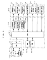
- Fig. 2 is a block diagram which shows the electric structure of the image forming apparatus which is shown in Fig. 1.
- This image forming apparatus is a color printer of the so-called 4-cycle type.
- an engine controller 10 controls respective portions of an engine part EG in accordance with the print instruction received from the main controller 11 of a CPU 111, and an image which corresponds to the print instruction is formed on a sheet which may be a copy paper, a transfer paper, a plain paper or a transparency for an overhead projector.
- a photosensitive member 2 is disposed so that the photosensitive member 2 can freely rotate in the arrow direction (sub scanning direction) shown in Fig. 1.
- a charger unit 3 Around the photosensitive member 2, a charger unit 3, a rotary developer unit 4 and a cleaner (not shown) are disposed along the direction in which the photosensitive member rotates.
- a charging controller 103 is electrically connected with the charger unit 3, for application of a predetermined charging bias upon the charger unit 3.
- the bias application uniformly charges an outer circumferential surface of the photosensitive member 2 to a predetermined surface potential.
- the photosensitive member 2, the charger unit 3 and the cleaner form one integrated photosensitive member cartridge which can be freely attached to and detached from a main body 5 as one integrated unit.
- An exposure unit 6 emits a light beam L toward the outer circumferential surface of the photosensitive member 2 thus charged by the charger unit 3.
- the exposure unit 6 makes the light beam L scan on the photosensitive member 2 based on an electric signal from an exposure controller which will be described later, whereby an electrostatic image which reflects an image signal is formed.
- the exposure unit 6 is thus an optical scanning apparatus according to the present invention, and the structure and operations of the exposure unit will be described in detail later.
- the developer unit 4 develops thus formed electrostatic latent image with toner.
- the developer unit 4 comprises a support frame 40 which is axially disposed for free rotations, and also a yellow developer 4Y, a magenta developer 4M, a cyan developer 4C and a black developer 4K which house toner of the respective colors and are formed as cartridges which are freely attachable to and detachable from the support frame 40.
- the developer unit 4 is driven into rotations in response to a control command given from a developer controller 104 of the engine controller 10.
- toner of the color corresponding to the selected developer is supplied onto the surface of the photosensitive member 2 by a developer roller 44 which carries the toner of the selected color.
- a developer roller 44 which carries the toner of the selected color.
- a toner image developed by the developer unit 4 in the manner above is primarily transferred onto an intermediate transfer belt 71 of a transfer unit 7 in a primary transfer region TR1.
- the transfer unit 7 comprises the intermediate transfer belt 71 which runs across a plurality of rollers 72, 73, etc., and a driver (not shown) which drives the roller 73 into rotations to thereby rotate the intermediate transfer belt 71 in a predetermined rotation direction.
- the density sensor 76 is disposed facing a surface of the intermediate transfer belt 71 and measures the optical density of a patch image formed on an outer circumferential surface of the intermediate transfer belt 71.
- the vertical synchronization sensor 77 is a sensor which detects a reference position of the intermediate transfer belt 71, and serves as a vertical synchronization sensor for obtaining a synchronizing signal outputted in relation to rotations of the intermediate transfer belt 71 in the sub scanning direction, namely, a vertical synchronizing signal Vsync.
- the respective portions of the apparatus operate under the control of the vertical synchronizing signal Vsync.
- the toner images of the respective colors formed on the photosensitive member 2 are overlaid each other on the intermediate transfer belt 71, thereby forming color images which will then be secondarily transferred onto sheets taken out one by one from a cassette 8 and transported on a transportation path F to a secondary transfer region TR2.
- the timing of feeding the sheet to the secondary transfer region TR2 is controlled.
- a gate roller 81 disposed in front of the secondary transfer region TR2 on the transportation path F, and as the gate roller 81 rotates in synchronization to the timing of rotations of the intermediate transfer belt 71, the sheet is fed into the secondary transfer region TR2 at predetermined timing.
- the sheet now bearing the color image is transported to a discharge tray part 51, which is disposed to a top surface portion of the main body 5, through a fixing unit 9 and a discharge roller 82.
- the discharge roller 82 moves the sheet seating an image on its one surface in the manner above in a switch back motion.
- the sheet is therefore transported along a reverse transportation path FR. While the sheet is returned back to the transportation path F again before arriving at the gate roller 81, the surface of the sheet which abuts on the intermediate transfer belt 71 in the secondary transfer region TR2 and is to receive a transferred image is, at this stage, the opposite surface to the surface which already bears the image. In this fashion, it is possible to form images on the both surfaces of the sheet.
- 113 is an image memory disposed in the main controller 11 for storage of image data fed from an external apparatus such as a host computer via an interface 112.
- Denoted at 106 is a ROM which stores a computation program executed by a CPU 101, control data for control of the engine part EG, etc.
- Denoted at 107 is a RAM which temporarily stores a computation result derived by the CPU 101, other data, etc.
- Fig. 3 is a main-scanning cross sectional view showing the structure of the exposure unit which is disposed in the image forming apparatus which is shown in Fig. 1.
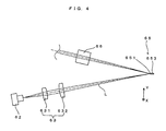
- Fig. 4 is a sub-scanning cross sectional view of the exposure unit.
- Fig. 5 is a perspective view which shows imaging of a scanning light beam.
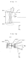
- Figs. 6 and 7 are drawings of a deflector which is one of components which form the exposure unit.
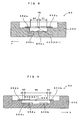
- Fig. 8 is a cross sectional view taken on line A - A of Fig. 7, and
- Fig. 9 is a cross sectional view taken on line B - B of Fig. 7.
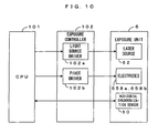
- Fig. 10 is a block diagram which shows the structures of the exposure unit and the exposure controller. The structure and operations of the exposure unit 6 will now be described in detail with reference to these drawings.
- the exposure unit 6 comprises an exposure housing 61.
- a single laser source 62 is fixed to the exposure housing 61, permitting emission of a light beam from the laser source 62.
- the laser source 62 is electrically connected with a light source driver 102a of an exposure controller 102 as shown in Fig. 10.
- the light source driver 102a controls ON and OFF of the laser source 62 in accordance with image data, and the laser source 62 emits a light beam modulated in accordance with the image data.
- the laser source 62 thus functions as the "light source" of the present invention.
- a collimator lens 631, a cylindrical lens 632, a mirror 64, a deflector 65, a scanning lens 66 and a return mirror 67 are disposed inside the exposure housing 61.
- the light beam from the laser source 62 impinges upon the cylindrical lens 632 which has power only in a sub scanning direction Y
- This collimated light is then converged only in the sub scanning direction Y and imaged in the shape of a line in the vicinity of a deflection mirror surface 651 of the deflector 65.
- the collimator lens 631 and the cylindrical lens 632 thus function as a first optical system 63 which shapes the light beam from the laser source 62 into an elongated cross sectional shape which is long in a main scanning direction X and makes the light beam impinge upon the deflection mirror surface 651.
- the deflector 65 is made using a micro machining technique which is an application of semiconductor manufacturing techniques and which aims at forming an integrated micro machine on a semiconductor substrate, and therefore, the deflector 65 is capable of deflecting a light beam reflected by the deflection mirror surface 651 in the main scanning direction X.
- the deflector 65 has the following structure.
- a frame member is formed which is obtained by processing a part of a single crystal substrate of silicon (hereinafter referred to a "silicon substrate") 652, the frame member being a combination of two horizontal side portions 652a and two vertical side portions 652b.
- the silicon substrate 652 is attached to a frame 650 in such a manner that the side portions 652a and 652b of the frame member cover the circumferential edge portion of the opening of a concave 650c which is formed in the frame 650 of the deflector 65.
- a movable plate 653 is disposed to the frame member so that the movable plate 653 can freely pivot about a pivot axis AX which elongates in the sub scanning direction Y which is approximately orthogonal to the main scanning direction X.
- the horizontal side portions 652a are apart by a first distance R1 from the movable plate 653 respectively on the both sides of the movable plate 653 in the direction Y of the pivot axis (Fig. 8), and the movable plate 653 is elastically supported to the horizontal side portions 652a of the silicon substrate 652 by torsion springs (beams) 654.
- the movable plate 653 is apart by a second distance R2 from the vertical side portions 652b (Fig. 9).
- the horizontal side portions 652a and the vertical side portions 652b correspond to the "first adjacent portions” and the “second adjacent portions” of the present invention respectively, and the movable plate 653 as it is apart from these can freely pivot about the pivot axis AX.
- a film of aluminum or the like is coated as the deflection mirror surface 651.
- the first distance R1 is longer than the second distance R2.
- the movable plate 653 has an elongated shape which is long in the main scanning direction X as shown in Fig. 6, and the width Hb of the movable plate 653 in the direction of the pivot axis (sub scanning direction) is shorter than the first distance R1. This will be described later.
- electrodes 658a and 658b are fixed at locations opposed against the both ends of the movable plate 653 (Figs. 8 and 9). These two electrodes 658a and 658b function as electrodes which are for driving the movable plate 653 into the pivoting action about the pivot axis AX.
- the electrodes 658a and 658b are electrically connected with a pivot driver 102b of the exposure controller 102, and when a voltage is applied to the electrode, electrostatic adsorption force acts between the electrode and the deflection mirror surface 651 so that one edge portion of the deflection mirror surface 651 is pulled toward the electrode.
- the electrodes 658a and 658b contributes to driving of the deflection mirror surface 651, and the edge portions of the deflection mirror surface 651 and the both electrodes disposed on a flat surface accordingly make it possible to more stably maintain the vibrations.
- an electrostatic adsorption force reciprocally vibrates the deflection mirror surface 651 according to this embodiment
- other diving method such as an electromagnetic force for instance may be used to vibrate the deflection mirror surface 651.
- Driving of the deflection mirror surface 651 by means of electromagnetic force is already a well known technique, and hence, will not be described here.
- the exposure unit 6 will be further described, referring back to Figs. 3 and 4.
- the scanning light beam which is made scan by the deflector 65 as described above is emitted from the deflector 65 toward the photosensitive member 2, and this scanning light beam is imaged on the photosensitive member 2 via the scanning lens 66 and the return mirror 67 which correspond to the "second optical system" of the present invention, and a spot of the light beam is consequently formed on the surface of the photosensitive member.
- the scanning light beam in this manner scans parallel to the main scanning direction X and a line-like latent image which elongates in the main scanning direction X is formed at a scan position 21 on the photosensitive member 2 as shown in Fig. 5.
- the synchronization sensor 60 functions as a horizontal synchronization reading sensor which is for obtaining a synchronizing signal in the main scanning direction X, namely, a horizontal synchronizing signal.
- first distance R1 and the second distance R2 The relationship between the first distance R1 and the second distance R2 will now be described. To begin with, needless to mention, shortening the first distance R1 and the second distance R2 is effective in reducing the size of the apparatus.
- heat develops around the movable plate 653 with the pivoting operation as described above.
- different countermeasures are taken in the direction of the pivot axis and in the main scanning direction in order to obviate the influence of the heat.
- the light beam L from the first optical system 63 is incident upon the deflection mirror surface 651 from the front side of the deflection mirror surface 651 and along the direction Y of the pivot axis at an acute angle with respect to the surface normal NL to the deflection mirror surface 651. Owing to this, the light beam L travels in the space other than the surrounding space SA mentioned above, namely, the space in the vicinity of the central section of the deflection mirror surface. This realizes scanning with the light beam without thermal influence.
- the size of the deflection mirror surface 651 along the main scanning direction X which is needed to cover a predetermined range of scanning is smaller than that in the conventional apparatus, and as a result, the length Ha of the movable plate 653 in the main scanning direction X is relatively short.
- the light beam L which is incident upon the deflection mirror surface 651 is shaped into an elongated cross sectional shape which elongates in the main scanning direction X by the first optical system 63, and the movable plate 653 is finished as an elongated strip which elongates in the main scanning direction X.
- the width Hb of the movable plate 653 in the direction of the pivot axis (the sub scanning direction Y) which is approximately orthogonal to the main scanning direction X is remarkably narrow.
- the weight of the movable plate 653 is lightened and the movable plate 653 can pivot stably at a faster speed than in the conventional apparatus. This allows that the light beam L scans on the surface of the photosensitive member 2 stably at a high speed and a latent image is formed in a stable manner.
- the present invention is not limited to the embodiment above, but may be modified in various manners in addition to the preferred embodiments above, to the extent not deviating from the object of the invention.
- the horizontal side portions (first adjacent portions) 652a, the vertical side portions (second adjacent portions) 652b, the movable plate 653 and the torsion springs (beams) 654 are made of the silicon substrate 652 in single-piece in the embodiment described above, the structure of the movable plate 653 and the torsion springs 654 is not limited to this.
- the present invention may be applicable to an exposure unit which comprises the deflector 65 in which the movable plate 653 and the torsion springs 654 are formed in single-piece and the single-piece unit is attached to the frame 650 as shown in Figs. 13 through 16 for instance.
- the respective torsion springs 654 are fixed to horizontal side portions 650a of the frame 650.
- the horizontal side portions 650a correspond to the "first adjacent portions” of the present invention while vertical side portions 650b of the frame 650 correspond to the "second adjacent portions" of the present invention.
- a magnetic force source such as a permanent magnet and an electromagnet is often disposed next to the movable plate 653 in the main scanning direction X.
- the magnetic force source corresponds to the "second adjacent portion" of the present invention.
- the light beam L is incident upon the deflection mirror surface 651 from below along the direction Y of the pivot axis, the light beam L may be incident from above along the direction of the pivot axis.
- the optical scanning apparatus according to the present invention is used as an exposure unit of a color image forming apparatus
- the present invention is not limited to this.
- the optical scanning apparatus according to the present invention may be used as an exposure unit of an image forming apparatus in which a light beam scans on a latent image carrier such as a photosensitive member to thereby form an electrostatic latent image, the electrostatic latent image is developed with toner and a toner image is formed.
- the application of the optical scanning apparatus is not limited to an exposure unit which is disposed to an image forming apparatus, but generally includes any optical scanning apparatus which makes a light beam scan on a surface-to-be-scanned.
Landscapes
- Physics & Mathematics (AREA)
- General Physics & Mathematics (AREA)
- Optics & Photonics (AREA)
- Engineering & Computer Science (AREA)
- Multimedia (AREA)
- Signal Processing (AREA)
- Facsimile Scanning Arrangements (AREA)
- Laser Beam Printer (AREA)
- Mechanical Optical Scanning Systems (AREA)
- Micromachines (AREA)
Applications Claiming Priority (2)
| Application Number | Priority Date | Filing Date | Title |
|---|---|---|---|
| JP2004029319 | 2004-02-05 | ||
| JP2004029319A JP2005221749A (ja) | 2004-02-05 | 2004-02-05 | 光走査装置および画像形成装置 |
Publications (2)
| Publication Number | Publication Date |
|---|---|
| EP1566956A1 true EP1566956A1 (de) | 2005-08-24 |
| EP1566956B1 EP1566956B1 (de) | 2007-11-21 |
Family
ID=34709074
Family Applications (1)
| Application Number | Title | Priority Date | Filing Date |
|---|---|---|---|
| EP05002255A Expired - Lifetime EP1566956B1 (de) | 2004-02-05 | 2005-02-03 | Optische Abtastvorrichtung und Bilderzeugungsgerät |
Country Status (5)
| Country | Link |
|---|---|
| US (1) | US7123396B2 (de) |
| EP (1) | EP1566956B1 (de) |
| JP (1) | JP2005221749A (de) |
| CN (1) | CN1323313C (de) |
| DE (1) | DE602005003381T2 (de) |
Cited By (1)
| Publication number | Priority date | Publication date | Assignee | Title |
|---|---|---|---|---|
| EP1821130A3 (de) * | 2006-02-15 | 2008-08-06 | Canon Kabushiki Kaisha | Optische Abtastvorrichtung und Bilderzeugungsvorrichtung damit |
Families Citing this family (8)
| Publication number | Priority date | Publication date | Assignee | Title |
|---|---|---|---|---|
| US7442918B2 (en) * | 2004-05-14 | 2008-10-28 | Microvision, Inc. | MEMS device having simplified drive |
| US7636101B2 (en) * | 2005-02-09 | 2009-12-22 | Microvision, Inc. | MEMS scanner adapted to a laser printer |
| EP1767982B1 (de) * | 2005-09-24 | 2009-11-11 | TRUMPF Laser GmbH + Co. KG | Ein-Spiegel-Scannervorrichtung für Hochleistungslaseranwendungen |
| JP4816026B2 (ja) * | 2005-11-22 | 2011-11-16 | セイコーエプソン株式会社 | 光走査装置および該装置を装備する画像形成装置 |
| JP5907048B2 (ja) * | 2012-12-07 | 2016-04-20 | ブラザー工業株式会社 | 光走査装置 |
| CN109477961B (zh) * | 2016-07-19 | 2021-02-26 | 麦克赛尔株式会社 | 投射型影像显示装置 |
| JP6880625B2 (ja) | 2016-09-29 | 2021-06-02 | セイコーエプソン株式会社 | 光スキャナー、画像表示装置、ヘッドマウントディスプレイおよびヘッドアップディスプレイ |
| CN112726449B (zh) * | 2020-12-17 | 2022-09-30 | 聊城市瀚格智能科技有限公司 | 一种具有自清洁功能的山路弯道球面镜 |
Citations (2)
| Publication number | Priority date | Publication date | Assignee | Title |
|---|---|---|---|---|
| JPS63279220A (ja) * | 1987-05-11 | 1988-11-16 | Konica Corp | 画像形成装置 |
| US20020163704A1 (en) * | 2001-03-01 | 2002-11-07 | Yoshinori Hayashi | Optical deflecting unit, optical scanning unit, image forming apparatus, and method of producing optical unit |
Family Cites Families (8)
| Publication number | Priority date | Publication date | Assignee | Title |
|---|---|---|---|---|
| US5010353A (en) * | 1986-07-04 | 1991-04-23 | Konica Corporation | Laser recorder with integrally molded deflector |
| US5629790A (en) * | 1993-10-18 | 1997-05-13 | Neukermans; Armand P. | Micromachined torsional scanner |
| JP3011144B2 (ja) * | 1997-07-31 | 2000-02-21 | 日本電気株式会社 | 光スキャナとその駆動方法 |
| US6331909B1 (en) * | 1999-08-05 | 2001-12-18 | Microvision, Inc. | Frequency tunable resonant scanner |
| JP4144840B2 (ja) * | 2001-02-22 | 2008-09-03 | キヤノン株式会社 | 揺動体装置、光偏向器、及び光偏向器を用いた光学機器 |
| JP2003222817A (ja) | 2002-01-30 | 2003-08-08 | Ricoh Co Ltd | 光走査装置、光走査モジュール及び画像形成装置 |
| JP2003315724A (ja) | 2002-04-26 | 2003-11-06 | Ricoh Co Ltd | 振動ミラーとその製造方法、光走査装置、画像形成装置 |
| US6972883B2 (en) * | 2002-02-15 | 2005-12-06 | Ricoh Company, Ltd. | Vibration mirror, optical scanning device, and image forming using the same, method for making the same, and method for scanning image |
-
2004
- 2004-02-05 JP JP2004029319A patent/JP2005221749A/ja not_active Withdrawn
-
2005
- 2005-01-17 CN CNB2005100023131A patent/CN1323313C/zh not_active Expired - Fee Related
- 2005-02-03 DE DE602005003381T patent/DE602005003381T2/de not_active Expired - Lifetime
- 2005-02-03 EP EP05002255A patent/EP1566956B1/de not_active Expired - Lifetime
- 2005-02-03 US US11/050,661 patent/US7123396B2/en not_active Expired - Fee Related
Patent Citations (2)
| Publication number | Priority date | Publication date | Assignee | Title |
|---|---|---|---|---|
| JPS63279220A (ja) * | 1987-05-11 | 1988-11-16 | Konica Corp | 画像形成装置 |
| US20020163704A1 (en) * | 2001-03-01 | 2002-11-07 | Yoshinori Hayashi | Optical deflecting unit, optical scanning unit, image forming apparatus, and method of producing optical unit |
Non-Patent Citations (1)
| Title |
|---|
| PATENT ABSTRACTS OF JAPAN vol. 013, no. 098 (P - 840) 8 March 1989 (1989-03-08) * |
Cited By (2)
| Publication number | Priority date | Publication date | Assignee | Title |
|---|---|---|---|---|
| EP1821130A3 (de) * | 2006-02-15 | 2008-08-06 | Canon Kabushiki Kaisha | Optische Abtastvorrichtung und Bilderzeugungsvorrichtung damit |
| US7646523B2 (en) | 2006-02-15 | 2010-01-12 | Canon Kabushiki Kaisha | Optical scanning apparatus and image forming apparatus using same |
Also Published As
| Publication number | Publication date |
|---|---|
| CN1323313C (zh) | 2007-06-27 |
| JP2005221749A (ja) | 2005-08-18 |
| US7123396B2 (en) | 2006-10-17 |
| CN1651970A (zh) | 2005-08-10 |
| DE602005003381T2 (de) | 2008-09-25 |
| US20050179974A1 (en) | 2005-08-18 |
| EP1566956B1 (de) | 2007-11-21 |
| DE602005003381D1 (de) | 2008-01-03 |
Similar Documents
| Publication | Publication Date | Title |
|---|---|---|
| US7570279B2 (en) | Optical scanning apparatus and image forming apparatus | |
| EP1553752B1 (de) | Optische Abtastvorrichtung und Bilderzeugungsgerät | |
| EP1566956B1 (de) | Optische Abtastvorrichtung und Bilderzeugungsgerät | |
| US7116457B2 (en) | Optical scanning apparatus and image forming apparatus | |
| EP1557710B1 (de) | Optische Abtastvorrichtung und Bilderzeugungsgerät | |
| JP2002131664A (ja) | 光走査装置及びそれを用いた画像形成装置 | |
| US7102805B2 (en) | Scanner having scan angle multiplier | |
| JP2011013331A (ja) | 光走査装置 | |
| JP4701593B2 (ja) | 光走査装置および画像形成装置 | |
| JP4075365B2 (ja) | 光走査装置 | |
| JP4483300B2 (ja) | 光走査装置および画像形成装置 | |
| JP4576816B2 (ja) | 光走査装置および画像形成装置 | |
| JP2009042494A (ja) | 光走査装置 | |
| JP4506087B2 (ja) | 画像形成装置 | |
| JP4453317B2 (ja) | 光走査装置および画像形成装置 | |
| JP2005115211A (ja) | 光走査装置および画像形成装置 | |
| JP2005062358A (ja) | 光走査装置および画像形成装置 | |
| JP4465967B2 (ja) | 画像形成装置 | |
| JP4483301B2 (ja) | 光走査装置および画像形成装置 | |
| JP2005181811A (ja) | 光走査装置および画像形成装置 | |
| JP2006337417A (ja) | 光走査装置および画像形成装置 | |
| JP2005208462A (ja) | 光走査装置および画像形成装置 | |
| JPH11183827A (ja) | 光偏向走査装置 | |
| JP2005070205A (ja) | 光走査装置および画像形成装置 |
Legal Events
| Date | Code | Title | Description |
|---|---|---|---|
| PUAI | Public reference made under article 153(3) epc to a published international application that has entered the european phase |
Free format text: ORIGINAL CODE: 0009012 |
|
| 17P | Request for examination filed |
Effective date: 20050627 |
|
| AK | Designated contracting states |
Kind code of ref document: A1 Designated state(s): AT BE BG CH CY CZ DE DK EE ES FI FR GB GR HU IE IS IT LI LT LU MC NL PL PT RO SE SI SK TR |
|
| AX | Request for extension of the european patent |
Extension state: AL BA HR LV MK YU |
|
| AKX | Designation fees paid |
Designated state(s): AT BE BG CH CY CZ DE DK EE ES FI FR GB GR HU IE IS IT LI LT LU MC NL PL PT RO SE SI SK TR |
|
| GRAP | Despatch of communication of intention to grant a patent |
Free format text: ORIGINAL CODE: EPIDOSNIGR1 |
|
| GRAS | Grant fee paid |
Free format text: ORIGINAL CODE: EPIDOSNIGR3 |
|
| GRAA | (expected) grant |
Free format text: ORIGINAL CODE: 0009210 |
|
| AK | Designated contracting states |
Kind code of ref document: B1 Designated state(s): AT BE BG CH CY CZ DE DK EE ES FI FR GB GR HU IE IS IT LI LT LU MC NL PL PT RO SE SI SK TR |
|
| REG | Reference to a national code |
Ref country code: GB Ref legal event code: FG4D |
|
| REG | Reference to a national code |
Ref country code: IE Ref legal event code: FG4D |
|
| REG | Reference to a national code |
Ref country code: CH Ref legal event code: EP |
|
| REF | Corresponds to: |
Ref document number: 602005003381 Country of ref document: DE Date of ref document: 20080103 Kind code of ref document: P |
|
| PG25 | Lapsed in a contracting state [announced via postgrant information from national office to epo] |
Ref country code: SE Free format text: LAPSE BECAUSE OF FAILURE TO SUBMIT A TRANSLATION OF THE DESCRIPTION OR TO PAY THE FEE WITHIN THE PRESCRIBED TIME-LIMIT Effective date: 20080221 Ref country code: CH Free format text: LAPSE BECAUSE OF FAILURE TO SUBMIT A TRANSLATION OF THE DESCRIPTION OR TO PAY THE FEE WITHIN THE PRESCRIBED TIME-LIMIT Effective date: 20071121 Ref country code: NL Free format text: LAPSE BECAUSE OF FAILURE TO SUBMIT A TRANSLATION OF THE DESCRIPTION OR TO PAY THE FEE WITHIN THE PRESCRIBED TIME-LIMIT Effective date: 20071121 Ref country code: LI Free format text: LAPSE BECAUSE OF FAILURE TO SUBMIT A TRANSLATION OF THE DESCRIPTION OR TO PAY THE FEE WITHIN THE PRESCRIBED TIME-LIMIT Effective date: 20071121 Ref country code: ES Free format text: LAPSE BECAUSE OF FAILURE TO SUBMIT A TRANSLATION OF THE DESCRIPTION OR TO PAY THE FEE WITHIN THE PRESCRIBED TIME-LIMIT Effective date: 20080304 |
|
| NLV1 | Nl: lapsed or annulled due to failure to fulfill the requirements of art. 29p and 29m of the patents act | ||
| PG25 | Lapsed in a contracting state [announced via postgrant information from national office to epo] |
Ref country code: BG Free format text: LAPSE BECAUSE OF FAILURE TO SUBMIT A TRANSLATION OF THE DESCRIPTION OR TO PAY THE FEE WITHIN THE PRESCRIBED TIME-LIMIT Effective date: 20080221 Ref country code: IS Free format text: LAPSE BECAUSE OF FAILURE TO SUBMIT A TRANSLATION OF THE DESCRIPTION OR TO PAY THE FEE WITHIN THE PRESCRIBED TIME-LIMIT Effective date: 20080321 Ref country code: FI Free format text: LAPSE BECAUSE OF FAILURE TO SUBMIT A TRANSLATION OF THE DESCRIPTION OR TO PAY THE FEE WITHIN THE PRESCRIBED TIME-LIMIT Effective date: 20071121 Ref country code: SI Free format text: LAPSE BECAUSE OF FAILURE TO SUBMIT A TRANSLATION OF THE DESCRIPTION OR TO PAY THE FEE WITHIN THE PRESCRIBED TIME-LIMIT Effective date: 20071121 Ref country code: LT Free format text: LAPSE BECAUSE OF FAILURE TO SUBMIT A TRANSLATION OF THE DESCRIPTION OR TO PAY THE FEE WITHIN THE PRESCRIBED TIME-LIMIT Effective date: 20071121 Ref country code: PL Free format text: LAPSE BECAUSE OF FAILURE TO SUBMIT A TRANSLATION OF THE DESCRIPTION OR TO PAY THE FEE WITHIN THE PRESCRIBED TIME-LIMIT Effective date: 20071121 |
|
| REG | Reference to a national code |
Ref country code: CH Ref legal event code: PL |
|
| ET | Fr: translation filed | ||
| PG25 | Lapsed in a contracting state [announced via postgrant information from national office to epo] |
Ref country code: AT Free format text: LAPSE BECAUSE OF FAILURE TO SUBMIT A TRANSLATION OF THE DESCRIPTION OR TO PAY THE FEE WITHIN THE PRESCRIBED TIME-LIMIT Effective date: 20071121 |
|
| PG25 | Lapsed in a contracting state [announced via postgrant information from national office to epo] |
Ref country code: DK Free format text: LAPSE BECAUSE OF FAILURE TO SUBMIT A TRANSLATION OF THE DESCRIPTION OR TO PAY THE FEE WITHIN THE PRESCRIBED TIME-LIMIT Effective date: 20071121 Ref country code: CZ Free format text: LAPSE BECAUSE OF FAILURE TO SUBMIT A TRANSLATION OF THE DESCRIPTION OR TO PAY THE FEE WITHIN THE PRESCRIBED TIME-LIMIT Effective date: 20071121 |
|
| PG25 | Lapsed in a contracting state [announced via postgrant information from national office to epo] |
Ref country code: SK Free format text: LAPSE BECAUSE OF FAILURE TO SUBMIT A TRANSLATION OF THE DESCRIPTION OR TO PAY THE FEE WITHIN THE PRESCRIBED TIME-LIMIT Effective date: 20071121 Ref country code: BE Free format text: LAPSE BECAUSE OF FAILURE TO SUBMIT A TRANSLATION OF THE DESCRIPTION OR TO PAY THE FEE WITHIN THE PRESCRIBED TIME-LIMIT Effective date: 20071121 Ref country code: RO Free format text: LAPSE BECAUSE OF FAILURE TO SUBMIT A TRANSLATION OF THE DESCRIPTION OR TO PAY THE FEE WITHIN THE PRESCRIBED TIME-LIMIT Effective date: 20071121 |
|
| PLBE | No opposition filed within time limit |
Free format text: ORIGINAL CODE: 0009261 |
|
| STAA | Information on the status of an ep patent application or granted ep patent |
Free format text: STATUS: NO OPPOSITION FILED WITHIN TIME LIMIT |
|
| PG25 | Lapsed in a contracting state [announced via postgrant information from national office to epo] |
Ref country code: PT Free format text: LAPSE BECAUSE OF FAILURE TO SUBMIT A TRANSLATION OF THE DESCRIPTION OR TO PAY THE FEE WITHIN THE PRESCRIBED TIME-LIMIT Effective date: 20080421 |
|
| 26N | No opposition filed |
Effective date: 20080822 |
|
| PG25 | Lapsed in a contracting state [announced via postgrant information from national office to epo] |
Ref country code: MC Free format text: LAPSE BECAUSE OF NON-PAYMENT OF DUE FEES Effective date: 20080228 |
|
| PG25 | Lapsed in a contracting state [announced via postgrant information from national office to epo] |
Ref country code: IE Free format text: LAPSE BECAUSE OF NON-PAYMENT OF DUE FEES Effective date: 20080204 Ref country code: GR Free format text: LAPSE BECAUSE OF FAILURE TO SUBMIT A TRANSLATION OF THE DESCRIPTION OR TO PAY THE FEE WITHIN THE PRESCRIBED TIME-LIMIT Effective date: 20080222 Ref country code: EE Free format text: LAPSE BECAUSE OF FAILURE TO SUBMIT A TRANSLATION OF THE DESCRIPTION OR TO PAY THE FEE WITHIN THE PRESCRIBED TIME-LIMIT Effective date: 20071121 |
|
| PG25 | Lapsed in a contracting state [announced via postgrant information from national office to epo] |
Ref country code: CY Free format text: LAPSE BECAUSE OF FAILURE TO SUBMIT A TRANSLATION OF THE DESCRIPTION OR TO PAY THE FEE WITHIN THE PRESCRIBED TIME-LIMIT Effective date: 20071121 |
|
| PG25 | Lapsed in a contracting state [announced via postgrant information from national office to epo] |
Ref country code: LU Free format text: LAPSE BECAUSE OF NON-PAYMENT OF DUE FEES Effective date: 20080203 Ref country code: HU Free format text: LAPSE BECAUSE OF FAILURE TO SUBMIT A TRANSLATION OF THE DESCRIPTION OR TO PAY THE FEE WITHIN THE PRESCRIBED TIME-LIMIT Effective date: 20080522 |
|
| PG25 | Lapsed in a contracting state [announced via postgrant information from national office to epo] |
Ref country code: TR Free format text: LAPSE BECAUSE OF FAILURE TO SUBMIT A TRANSLATION OF THE DESCRIPTION OR TO PAY THE FEE WITHIN THE PRESCRIBED TIME-LIMIT Effective date: 20071121 |
|
| PG25 | Lapsed in a contracting state [announced via postgrant information from national office to epo] |
Ref country code: IT Free format text: LAPSE BECAUSE OF NON-PAYMENT OF DUE FEES Effective date: 20080229 |
|
| PGFP | Annual fee paid to national office [announced via postgrant information from national office to epo] |
Ref country code: DE Payment date: 20140129 Year of fee payment: 10 |
|
| PGFP | Annual fee paid to national office [announced via postgrant information from national office to epo] |
Ref country code: FR Payment date: 20140211 Year of fee payment: 10 |
|
| PGFP | Annual fee paid to national office [announced via postgrant information from national office to epo] |
Ref country code: GB Payment date: 20140129 Year of fee payment: 10 |
|
| REG | Reference to a national code |
Ref country code: DE Ref legal event code: R119 Ref document number: 602005003381 Country of ref document: DE |
|
| GBPC | Gb: european patent ceased through non-payment of renewal fee |
Effective date: 20150203 |
|
| REG | Reference to a national code |
Ref country code: FR Ref legal event code: ST Effective date: 20151030 |
|
| PG25 | Lapsed in a contracting state [announced via postgrant information from national office to epo] |
Ref country code: DE Free format text: LAPSE BECAUSE OF NON-PAYMENT OF DUE FEES Effective date: 20150901 Ref country code: GB Free format text: LAPSE BECAUSE OF NON-PAYMENT OF DUE FEES Effective date: 20150203 |
|
| PG25 | Lapsed in a contracting state [announced via postgrant information from national office to epo] |
Ref country code: FR Free format text: LAPSE BECAUSE OF NON-PAYMENT OF DUE FEES Effective date: 20150302 |