EP1566835B1 - Isolationsfilmmaterial mit organischer silan- oder organischersiloxanzusammensetzung, verfahren zu seiner herstellung und halbleiterbauelement - Google Patents
Isolationsfilmmaterial mit organischer silan- oder organischersiloxanzusammensetzung, verfahren zu seiner herstellung und halbleiterbauelement Download PDFInfo
- Publication number
- EP1566835B1 EP1566835B1 EP03775970A EP03775970A EP1566835B1 EP 1566835 B1 EP1566835 B1 EP 1566835B1 EP 03775970 A EP03775970 A EP 03775970A EP 03775970 A EP03775970 A EP 03775970A EP 1566835 B1 EP1566835 B1 EP 1566835B1
- Authority
- EP
- European Patent Office
- Prior art keywords
- insulating film
- atom
- group
- hydrocarbon group
- formula
- Prior art date
- Legal status (The legal status is an assumption and is not a legal conclusion. Google has not performed a legal analysis and makes no representation as to the accuracy of the status listed.)
- Expired - Lifetime
Links
- 0 CCC(C)(*(*)*)[N+]I Chemical compound CCC(C)(*(*)*)[N+]I 0.000 description 1
Classifications
-
- H—ELECTRICITY
- H01—ELECTRIC ELEMENTS
- H01B—CABLES; CONDUCTORS; INSULATORS; SELECTION OF MATERIALS FOR THEIR CONDUCTIVE, INSULATING OR DIELECTRIC PROPERTIES
- H01B3/00—Insulators or insulating bodies characterised by the insulating materials; Selection of materials for their insulating or dielectric properties
- H01B3/18—Insulators or insulating bodies characterised by the insulating materials; Selection of materials for their insulating or dielectric properties mainly consisting of organic substances
- H01B3/30—Insulators or insulating bodies characterised by the insulating materials; Selection of materials for their insulating or dielectric properties mainly consisting of organic substances plastics; resins; waxes
- H01B3/46—Insulators or insulating bodies characterised by the insulating materials; Selection of materials for their insulating or dielectric properties mainly consisting of organic substances plastics; resins; waxes silicones
-
- H10P14/6922—
-
- C—CHEMISTRY; METALLURGY
- C07—ORGANIC CHEMISTRY
- C07F—ACYCLIC, CARBOCYCLIC OR HETEROCYCLIC COMPOUNDS CONTAINING ELEMENTS OTHER THAN CARBON, HYDROGEN, HALOGEN, OXYGEN, NITROGEN, SULFUR, SELENIUM OR TELLURIUM
- C07F7/00—Compounds containing elements of Groups 4 or 14 of the Periodic Table
- C07F7/02—Silicon compounds
- C07F7/08—Compounds having one or more C—Si linkages
- C07F7/18—Compounds having one or more C—Si linkages as well as one or more C—O—Si linkages
- C07F7/1804—Compounds having Si-O-C linkages
- C07F7/1872—Preparation; Treatments not provided for in C07F7/20
- C07F7/1876—Preparation; Treatments not provided for in C07F7/20 by reactions involving the formation of Si-C linkages
-
- C—CHEMISTRY; METALLURGY
- C07—ORGANIC CHEMISTRY
- C07F—ACYCLIC, CARBOCYCLIC OR HETEROCYCLIC COMPOUNDS CONTAINING ELEMENTS OTHER THAN CARBON, HYDROGEN, HALOGEN, OXYGEN, NITROGEN, SULFUR, SELENIUM OR TELLURIUM
- C07F7/00—Compounds containing elements of Groups 4 or 14 of the Periodic Table
- C07F7/02—Silicon compounds
- C07F7/21—Cyclic compounds having at least one ring containing silicon, but no carbon in the ring
-
- C—CHEMISTRY; METALLURGY
- C23—COATING METALLIC MATERIAL; COATING MATERIAL WITH METALLIC MATERIAL; CHEMICAL SURFACE TREATMENT; DIFFUSION TREATMENT OF METALLIC MATERIAL; COATING BY VACUUM EVAPORATION, BY SPUTTERING, BY ION IMPLANTATION OR BY CHEMICAL VAPOUR DEPOSITION, IN GENERAL; INHIBITING CORROSION OF METALLIC MATERIAL OR INCRUSTATION IN GENERAL
- C23C—COATING METALLIC MATERIAL; COATING MATERIAL WITH METALLIC MATERIAL; SURFACE TREATMENT OF METALLIC MATERIAL BY DIFFUSION INTO THE SURFACE, BY CHEMICAL CONVERSION OR SUBSTITUTION; COATING BY VACUUM EVAPORATION, BY SPUTTERING, BY ION IMPLANTATION OR BY CHEMICAL VAPOUR DEPOSITION, IN GENERAL
- C23C16/00—Chemical coating by decomposition of gaseous compounds, without leaving reaction products of surface material in the coating, i.e. chemical vapour deposition [CVD] processes
- C23C16/22—Chemical coating by decomposition of gaseous compounds, without leaving reaction products of surface material in the coating, i.e. chemical vapour deposition [CVD] processes characterised by the deposition of inorganic material, other than metallic material
- C23C16/30—Deposition of compounds, mixtures or solid solutions, e.g. borides, carbides, nitrides
- C23C16/40—Oxides
- C23C16/401—Oxides containing silicon
-
- B—PERFORMING OPERATIONS; TRANSPORTING
- B05—SPRAYING OR ATOMISING IN GENERAL; APPLYING FLUENT MATERIALS TO SURFACES, IN GENERAL
- B05D—PROCESSES FOR APPLYING FLUENT MATERIALS TO SURFACES, IN GENERAL
- B05D1/00—Processes for applying liquids or other fluent materials
- B05D1/62—Plasma-deposition of organic layers
-
- H10P14/6336—
-
- H10P14/665—
-
- H10P14/6682—
-
- H10P14/6686—
Definitions
- the present invention relates to a low dielectric constant interlayer insulating film material used in multilayer interconnect technology in logic ULSI. Particularly, it relates to a material for insulating film composed of organosilicon compound of an organosilane compound for plasma polymerization, and its use.
- the low dielectric constant interlayer insulating film material various ones have been proposed.
- the inorganic system silicon dioxide (SiO 2 ), silicon nitride and phosphosilicate glass, and as the organic system, polyimides have been employed.
- a method of forming the insulating film there are two methods including a coating method comprising coating an insulating film polymer solution by e.g. spin coating to carry out film formation and a CVD method comprising plasma polymerization mainly in a plasma CVD equipment to carry out film formation.
- JP-A-2002-110670 proposes a method of forming an oxidized trimethylsilane thin film from trimethylsilane and oxygen by the plasma CVD method.
- JP-A-11-288931 proposes a method of forming an oxidized alkylsilane thin film from an alkoxysilane having a straight chain alkyl group such as methyl, ethyl or n-propyl, an alkynyl group such as vinyl phenyl and an aryl group, by the plasma CVD method.
- An insulating film formed by such conventional plasma CVD material has favorable adhesion properties to a barrier metal and a copper wiring material which is a wiring material, on the contrary, uniformity of the film may be problematic, or the film deposition rate or the dielectric constant may be insufficient in some cases.
- the film formed by the coating method has favorable uniformity, however, three steps of coating, solvent removal and heat treatment are required, such being economically disadvantageous as compared with a film formed by the CVD method. Further, adhesion properties to a barrier metal and a copper wiring material which is a wiring material, and uniform coating itself of the coating liquid to a miniaturized substrate structure tend to be problematic in many cases.
- a method of making materials be porous has been proposed so as to achieve an ultra low-k material having a dielectric constant of at most 2.5, more preferably at most 2.0.
- a method of dispersing organic component fine particles which are easily pyrolyzed into an organic or inorganic material matrix, followed by heat treatment to make the material be porous, and a method of depositing SiO 2 ultrafine particles formed by evaporation of silicon and oxygen in a gas, to form a thin film of SiO 2 ultrafine particles, may, for example, be mentioned.
- the market further requires a well-balanced material which satisfies all the requirements such as a low dielectric constant, an adequate mechanical strength, adhesion properties to a barrier metal, prevention of copper dispersion, plasma ashing resistance and moisture absorption resistance.
- a well-balanced material which satisfies all the requirements such as a low dielectric constant, an adequate mechanical strength, adhesion properties to a barrier metal, prevention of copper dispersion, plasma ashing resistance and moisture absorption resistance.
- an organosilane type material having an increased proportion of carbon in the organic substituent to silane, thereby having characteristics intermediate between the organic polymer and the inorganic polymer has been proposed.
- JP-A-2000-302791 proposes a method to obtain an interlayer insulating film not being porous and having a dielectric constant of at most 2.4, by using a coating solution obtained by hydrolysis and polycondensation of a silicon compound having an adamantyl group by a sol-gel method in the presence of an aqueous acid solution.
- this material is a material for the coating method, and there are still problems of the above-described film formation method by the film coating method.
- Tamao Kohei et al., Tetrahedron Letters, Vo. 25, No. 18, pp 1905-1908 (1984 ) discuss the reactivity of vinylsilane by the structural analysis of the LUMO of the vinyl group, with the aim to attain the addition of n-alkyl Grignard reagents to silafunctional vinylsilane, but have observed that when reacting vinyltriethoxysilane with isopropyl Grignard reagent, unfortunately substitution predominates, thus leading to formation of isopropylvinyldiethoxysilane.
- a material containing an organic silicon Compound for use in making an interlager insulating film is disclosed in EP-A-0826791 .
- the present invention has been made to solve the above problems, and it is an object of the present invention to provide a novel low dielectric constant material, particularly a material for a low dielectric constant insulating film, containing organosilicon compound of an organosilane compound , suitable for a PECVD equipment, and to provide an insulating film employing it, and a semiconductor device containing such an insulating film.
- organosilicon compound of an organosilane compound having such a structure that a secondary hydrocarbon group and an alkenyl group is directly bonded to a silicon atom is suitable as a material for an insulating film, particularly a low dielectric constant interlayer insulating film for a semiconductor device, and accomplished the present invention.
- the present invention resides in a material for insulating film comprising an organosilicon compound , from which an insulating film is formed by chemical vapor deposition of the organosilicon compound, wherein said organosilicon compound is an organosilane compound represented by the following formula (1) having such a structure that a secondary hydrocarbon group and an alkenyl group are directly bonded to a silicon atom: wherein each of R 1 and R 2 represents a C 1-20 hydrocarbon group, R 3 represents a C 1-20 hydrocarbon group having at least one alkenyl group, or an alkenyl group and an aryl group, R 4 represents a C 1-10 hydrocarbon group or a hydrogen atom, m represents an integer of from 1 to 2, n represents an integer of from 1 to 2, and m+n represents an integer of from 2 to 3.
- organosilicon compound is an organosilane compound represented by the following formula (1) having such a structure that a secondary hydrocarbon group and an alkenyl group are directly bonded to a silicon atom
- each of R 1 and R 2 is a C 1-20 saturated or unsaturated hydrocarbon group, and may have any of straight chain, branched chain and cyclic structures. Further, a structure that groups bond to each other is included in the present invention. If the carbon number exceeds 20, it tends to be difficult to obtain a material such as a corresponding organic halide, or even if it can be obtained, the purity tends to be low in some cases.
- a C 1-10 hydrocarbon group is particularly preferred from such a viewpoint that the vapor pressure of the organosilane compound will not be too low.
- Examples of the hydrocarbon group for each of R 1 and R 2 are not particularly limited, and a C 1-20 , preferably C 1-10 , alkyl group, an aryl group, an arylalkyl group and an alkylaryl group may be mentioned.
- R 1 and R 2 may be the same or different.
- a secondary hydrocarbon group may be mentioned wherein R 1 and R 2 are at least one member or at least two members selected from the group consisting of methyl, ethyl, n-propyl, isopropyl, n-butyl, i-butyl, sec-butyl, tert-butyl, n-pentyl, tert-amyl, n-hexyl, cyclohexyl, phenyl and toluyl groups.
- a secondary hydrocarbon group in a group in which R 1 and R 2 are bonded to each other and bonded to Si by means of secondary carbon examples of a secondary hydrocarbon group in a group in which R 1 and R 2 are bonded to each other and bonded to Si by means of secondary carbon
- cyclobutyl, cyclobutenyl, cyclopentyl, cyclopentadienyl, cyclohexyl, cyclohexenyl, cyclooctenyl and cyclooctadienyl groups may be mentioned as typical examples.
- R 1 and R 2 an iso-propyl group wherein R 1 and R 2 are both methyl, a sec-butyl group wherein R 1 and R 2 are methyl and ethyl, and cyclopentyl, cyclopentadienyl, cyclohexyl and cyclohexenyl groups wherein R 1 and R 2 are bonded to each other, are preferred from an economical viewpoint.
- R 3 is a C 1-20 hydrocarbon group having at least one alkenyl group, or an alkenyl group and an aryl group.
- alkenyl group vinyl, 1-propenyl, 1-butenyl, 1-pentenyl, 1-hexenyl, 2-propenyl, 2-butenyl, 2-pentenyl and 2-hexenyl may be mentioned as typical examples.
- the alkenyl group is preferably a vinyl group.
- the hydrocarbon group other than the alkenyl group a C 1-20 hydrocarbon group other than an aryl group, such as the same group as R 1 and R 2 may be mentioned.
- R 4 represents a C 1-10 hydrocarbon group or a hydrogen atom, and the hydrocarbon group may be a saturated or unsaturated hydrocarbon group, and may have any of straight chain, branched chain and cyclic structures. If the carbon number exceeds 10, the vapor pressure of the formed organosilane tends to be low and its use in a PECVD equipment may be difficult in some cases, such being unfavorable.
- R 4 is preferably methyl, ethyl, n-propyl, isopropyl, n-butyl, i-butyl, sec-butyl or tert-butyl which is a C 1-4 hydrocarbon group in view of preparation of the material.
- n represents an integer of from 1 to 3
- m+n represents an integer of 3 or under.
- a mixture thereof is included in the present invention.
- organosilane compound represented by the above formula (1) examples include:
- the method for producing the organosilane compound of the above formula (1) is not particularly limited.
- the organosilane compound represented by the formula (1) can be produced by reacting an organic compound represented by the following formula (5): wherein R 1 and R 2 are as defined above, and X represents a hydrogen atom, a chlorine atom, a bromine atom or an iodine atom, with organolithium or metal lithium granule to produce a compound in which a secondary hydrocarbon group and a lithium atom are directly bonded, and reacting this compound with a halogenated organosilane or a halogenated organoalkoxysilane represented by the following formula (6): X' p SiR 3 q (OR 4 ) 4-(p+q) formula (6) wherein X' represents a fluorine atom, a chlorine atom, a bromine atom or an iodine atom, R 3 and R 4 are as defined above, p represents an integer of from 0 to 4,
- organosilane compound represented by the formula (1) can be produced by using metal magnesium instead of the organolithium or the metal lithium granule in the above production method.
- Examples of the organic compound represented by the formula (5) wherein X is a chlorine atom, a bromine atom or an iodine atom include isopropyl chloride, isopropyl bromide, isopropyl iodide, sec-butyl chloride, sec-butyl bromide, sec-butyl iodide, cyclopentyl chloride, cyclopentyl bromide, cyclopentyl iodide, cyclohexyl chloride, cyclohexyl bromide and cyclohexyl iodide.
- examples of the organic compound represented by the formula (5) wherein X is a hydrogen atom include cyclopentadiene, pentamethylcyclopentadiene and 1,2,3,4-tetramethyl-1,3-cyclopentadiene.
- organolithium such as n-butyl lithium or tert-butyl lithium
- a compound in which a secondary hydrocarbon group and a lithium atom are directly bonded can be produced.
- halogenated organosilane, halogenated organoalkoxysilane or tetraalkoxysilane represented by the formula (6) examples include vinyltriethoxysilane, vinyltrimethoxysilane, divinyldimethoxysilane, divinyldiethoxysilane, vinylmethyldimethoxysilane, vinylethyldimethoxysilane, vinyl n-propyldimethoxysilane, vinyl n-butyldimethoxysilane, vinylmethyldimethoxysilane, vinylethyldimethoxysilane, vinyl n-propyldimethoxysilane, vinyl n-butyldimethoxysilane, vinyltrichlorosilane, divinyldichlorosilane, vinylmethyldichlorosilane, vinylethyldichlorosilane, vinylmethyldichlorosilane, vinylethyldichlorosilane, vinylmethyl
- alkali metal alkoxide represented by the formula (7) examples include lithium methoxide, lithium ethoxide, lithium-i-propoxide, sodium methoxide, sodium ethoxide, sodium-i-propoxide, potassium methoxide, potassium ethoxide, potassium-i-propoxide and potassium-tert-butoxide.
- the organosilane compound represented by the formula (1) with a high purity can be obtained with a high yield while suppressing formation of by-products.
- the conditions for production of the compound in which a secondary hydrocarbon group and a lithium atom are directly bonded are not particularly limited, and one example is shown below.
- a lithium wire, a lithium ribbon or a lithium shot may, for example, be employed, and it is preferred to employ lithium fine particles having a particle size of at most 500 ⁇ m in view of reaction efficiency.
- a magnesium ribbon, magnesium granule or a magnesium powder may, for example, be employed.
- n-hexane solution of n-butyl lithium or a n-pentane solution of tert-butyl lithium may, for example, be employed.
- the solvent to be used for the reaction is not particularly limited so long as it is used for said technical field.
- a saturated hydrocarbon such as n-pentane, i-pentane, n-hexane, cyclohexane, n-heptane or n-decane, an unsaturated hydrocarbon such as toluene, xylene or decene-1, or an ether such as diethyl ether, dipropyl ether, tert-butyl methyl ether, dibutyl ether or cyclopentyl methyl ether, may be used.
- a mixed solvent thereof may also be used.
- the reaction temperature for the above reaction is preferably such a temperature range that the formed compound in which a secondary carbon atom and a lithium atom are bonded, or compound in which a secondary hydrocarbon group and a magnesium atom are directly bonded, will not decompose.
- the reaction is preferably carried out usually at a temperature of from -100 to 200°C which is industrially employed, preferably at a temperature of from -85 to 150°C.
- the pressure condition of the reaction the reaction may be carried out under elevated pressure, normal pressure or reduced pressure.
- the prepared compound in which a secondary hydrocarbon group and a lithium atom are directly bonded or compound in which a secondary hydrocarbon group and a magnesium atom are directly bonded may be used as it is after the production, or it may be used after unreacted organic halide, metal lithium or metal magnesium, and lithium halide or magnesium halide as a reaction by-product are removed.
- the conditions of the reaction of the compound in which a secondary hydrocarbon group and a lithium atom are directly bonded or compound in which a secondary hydrocarbon group and a magnesium atom are directly bonded thus obtained, and the halogenated organosilane or the halogenated organoalkoxysilane of the above formula (6), are not particularly limited, and one example is shown below.
- reaction solvent to be used the same solvents as the solvents which can be used for the production of the above compound in which a secondary hydrocarbon group and a lithium atom (or a magnesium atom) are directly bonded may be used.
- the reaction temperature is preferably such a temperature range that the compound in which a secondary hydrocarbon group and/or an alkenyl group and a lithium atom (or a magnesium atom) are directly bonded, will not decompose.
- the reaction is preferably carried out usually at a temperature of from -100 to 200°C which is industrially employed, preferably at a temperature of from -85 to 150°C.
- the pressure condition of the reaction the reaction may be carried out under elevated pressure, normal pressure or reduced pressure.
- the moisture content is less than 50 ppm and that the content of impurity elements other than silicon, carbon, oxygen and hydrogen, derived from reactant materials, is less than 10 ppb. Accordingly, it is preferred to purify such an organosilicon compound by means of filtration using e.g. a glass filter or a sintered porous body, distillation under normal pressure or under reduced pressure, or column separation using silica, alumina or a polymer gel, to remove lithium salts or magnesium salts as by-products. In such a case, as the case requires, the above purification means may be used in combination.
- hydroxyl groups of the silanol are treated with e.g. sodium hydride or potassium hydride so that the by-product is precipitated in a form of a sodium salt or a potassium salt, and then the alkoxysilane substituted by a hydrocarbon group as the main product can be isolated by distillation.
- the operation is in accordance with a method in the field of said organometal compound synthesis. Namely, it is preferred that the reaction is carried out in an atmosphere of dehydrated and deoxidized nitrogen or argon, and a solvent, a column packing material for purification, etc., to be used are preliminarily subjected to dehydration operation. Further, it is preferred that impurities such as metal residue and particles are removed.
- the organosilane compounds represented by the formula (1) of the present invention are materials suitable as a material for low dielectric constant insulating film formation by a PECVD equipment.
- the method for forming the insulating film material of the present invention is not particularly limited.
- a PECVD equipment which is commonly used in the field of said technology such as a semiconductor production field or a liquid crystal display production field, is used to form an insulating film.
- the PECVD equipment means an equipment in which a material for insulating film such as an organosilane is vaporized by a vaporizer and introduced to the inside of a film formation chamber, and a voltage is applied to an electrode in the film formation chamber by a high frequency power source to generate plasma, to form a plasma polymerization film on e.g. a silicon substrate in the film formation chamber.
- a gas such as argon or helium or an oxidizing agent such as oxygen or nitrous oxide may be introduced.
- a thin film suitable as a low dielectric constant material (low-k material) for a semiconductor device can be formed.
- a porous low dielectric constant insulating film can be obtained also by forming the material of the formula (1) into a film by CVD, and then subjecting the film to a heat treatment at a temperature of 350 deg.°C or over at which bond between one of the secondary hydrocarbon group, the alkenyl group, the alkyl group and the aryl group and the silicon atom is broken.
- the heat treatment temperature is preferably 350 deg.°C or over at which formation into a porous body is completed, and 500 deg.°C or under at which a semiconductor device will not deteriorate.
- the low dielectric-constant material of the present invention is suitable for production of ULSI employing multilayer interconnect, and a semiconductor device employing it is also included in the present invention.
- the isolated isopropylvinyldimethoxysilane was analyzed by 1 H-NMR, 13 C -NMR and GC-MS, and the results were as follows.
- the isolated divinyl di-tert-butoxysilane was analyzed by 1 H-NMR and GC-MS, and the results were as follows.
- the film was a thin film having a high proportion of carbon (organic substituent) relative to silicon, suitable as a material for insulating film.
- Example 3 except that dimethyldimethoxysilane was used as the monomer to be polymerized. The results are shown below.
- the film formation rate was low and the proportion of carbon (organic substituent) relative to silicon was low as compared with Example 3, and only a thin film unsuitable as a material for insulating film was obtained.
- Film formation by plasma polymerization was carried out on a silicon substrate in the same manner as in Example 3 except that isopropylvinyldimethoxysilane was used as the monomer to be polymerized. The results are shown below.
- the obtained film was a thin film having a high proportion of carbon (organic substituent) relative to silicon, suitable as a material for insulating film.
- a material having a low dielectric constant and high mechanical strength can be provided as a low dielectric constant material for an interlayer insulating film of a semiconductor device, by using an organosilane compound having such a structure that a secondary hydrocarbon group and an alkenyl group is directly bonded to a silicon atom of the present invention.
- an organosilane compound having such a structure that a secondary hydrocarbon group and an alkenyl group is directly bonded to a silicon atom useful as a material for interlayer insulating film by a PECVD method, can be efficiently produced with high purity.
Landscapes
- Chemical & Material Sciences (AREA)
- Organic Chemistry (AREA)
- Chemical Kinetics & Catalysis (AREA)
- Materials Engineering (AREA)
- General Chemical & Material Sciences (AREA)
- Engineering & Computer Science (AREA)
- Inorganic Chemistry (AREA)
- Mechanical Engineering (AREA)
- Metallurgy (AREA)
- Physics & Mathematics (AREA)
- Spectroscopy & Molecular Physics (AREA)
- Formation Of Insulating Films (AREA)
- Chemical Vapour Deposition (AREA)
Claims (15)
- Material für Isolierfolie, umfassend eine Organosiliziumverbindung, aus dem die Isolierfolie durch chemische Gasphasenabscheidung der Organosiliziumverbindung ausgebildet ist,
wobei die Organosiliziumverbindung eine Organosilanverbindung ist, die durch Formel (1) dargestellt ist und eine derartige Struktur aufweist, dass eine sekundäre Kohlenwasserstoffgruppe und eine Alkenylgruppe direkt an ein Siliziumatom gebunden sind:
mit der Maßgabe, dass die Organosiliziumverbindung nicht Isopropylvinyldiethoxysilan ist. - Material für Isolierfolie nach Anspruch 1, wobei die sekundäre Kohlenwasserstoffgruppe in der Formel (1) Isopropyl, Sec-Butyl, Cyclopentyl, Cyclohexyl, Cyclohexenyl oder Cyclopentadienyl ist.
- Material für Isolierfolie nach Anspruch 2, wobei eine Vinylgruppe und eine Isopropylgruppe an dasselbe Siliziumatom in der Formel (1) gebunden sind.
- Material für Isolierfolie nach Anspruch 1, wobei die Organosiliziumverbindung der Formel (1) Isopropylvinyldimethoxysilan ist.
- Material für Isolierfolie nach Anspruch 1, das einen Unreinheitsgehalt, der sich aus Reaktionspartnermaterialien ableitet, welches Elemente außer Silizium, Kohlenstoff, Sauerstoff und Wasserstoff sind, von weniger als 10 ppb aufweist und einen Feuchtigkeitsgehalt von weniger als 50 ppm aufweist.
- Material für Isolierfolie nach Anspruch 1, wobei die chemische Gasphasenabscheidung plasmaunterstützte chemische Gasphasenabscheidung (PECVD) ist.
- Verfahren zum Erzeugen der Organosiliziumverbindung, die durch die Formel (1) dargestellt ist, wie in Anspruch 1 definiert:


X' pSiR3 q (OR4)4-(p+q) Formel (6)
wobei X' ein Fluoratom, ein Chloratom, ein Bromatom oder ein Iodatom darstellt, R3 und R4 wie obenstehend definiert sind, p eine Ganzzahl von 0 bis 4 darstellt, q eine Ganzzahl von 1 bis 2 darstellt, und p+q eine Ganzzahl von 4 oder darunter darstellt, und wenn ein Halogenatom direkt an Silizium gebunden verbleibt, ein Alkalimetallalkoxid, das durch die folgende Formel (7) dargestellt ist, zur Reaktion damit bringen:
R4OM Formel (7)
wobei M ein Alkalimetall ist, und R4 wie obenstehend definiert ist, und Ausführen von Reinigung durch Filtration, Destillation oder Spaltentrennung umfasst. - Isolierfolie, die durch eine PECVD-Ausrüstung unter Benutzung eines Materials für Isolierfolie ausgebildet ist, umfassend eine Organosiliziumverbindung, aus dem eine Isolierfolie durch chemische Gasphasenabscheidung der Organosiliziumverbindung ausgebildet ist,
wobei die Organosiliziumverbindung eine Organosilanverbindung ist, die durch Formel (1) dargestellt ist und eine derartige Struktur aufweist, dass eine sekundäre Kohlenwasserstoffgruppe und eine Alkenylgruppe direkt an ein Siliziumatom gebunden sind: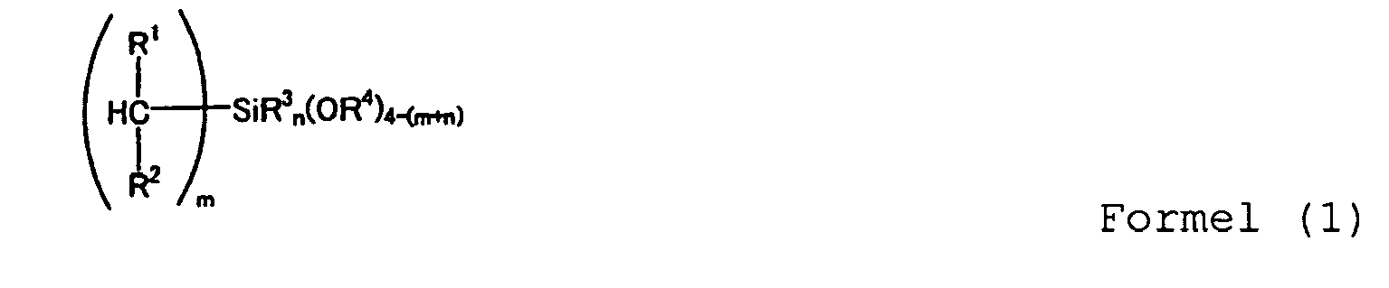
- Isolierfolie nach Anspruch 8, wobei die sekundäre Kohlenwasserstoffgruppe in der Formel (1) Isopropyl, Sec-butyl, Cyclopentyl, Cyclohexyl, Cyclohexenyl oder Cyclopentadienyl ist.
- Isolierfolie nach Anspruch 8, wobei eine Vinylgruppe und eine Isopropylgruppe an dasselbe Siliziumatom in der Formel (1) gebunden sind.
- Isolierfolie nach Anspruch 8, wobei die Organosiliziumverbindung der Formel (1) Isopropylvinyldimethoxysilan ist.
- Isolierfolie nach Anspruch 8, wobei das Material für Isolierfolie einen Unreinheitsgehalt, der sich aus Reaktionspartnermaterialien ableitet, welches Elemente außer Silizium, Kohlenstoff, Sauerstoff und Wasserstoff sind, von weniger als 10 ppb aufweist und einen Feuchtigkeitsgehalt von weniger als 50 ppm aufweist.
- Isolierfolie nach einem der Ansprüche 8 bis 12, die durch Unterziehen der Isolierfolie einer Wärmebehandlung auf einer Temperatur von zumindest einer Temperatur zu einem porösen Körper ausgebildet ist, auf der die Bindung zwischen einem Siliziumatom und einem von einer sekundären Kohlenwasserstoffgruppe, einer Alkylgruppe, einer Alkenylgruppe und einer Arylgruppe gebrochen wird.
- Halbleiterbauelement unter Benutzung der Isolierfolie wie in einem der Ansprüche 8 bis 13 definiert.
- Verbindung, die aus der Gruppe von Isopropylvinyldimethoxysilan, Isopropylvinyl-di-tert-butoxysilan, Diisopropylvinylmethoxysilan, Diisopropylvinylethoxysilan, Diisopropylvinyl-tert-butoxysilan, Sec-butylvinyldimethoxysilan, Secbutylvinyldiethoxysilan, Sec-butylvinyl-di-tert-butoxysilan, Di-sec-butylvinylmethoxysilan, Di-secbutylvinylethoxysilan, Di-sec-butylvinyl-tert-butoxysilan ausgewählt ist.
Priority Applications (1)
| Application Number | Priority Date | Filing Date | Title |
|---|---|---|---|
| EP10191051.1A EP2278612B1 (de) | 2002-11-28 | 2003-11-28 | Isolationsfilmmmaterial mit organischer Silan oder organischer Siloxanverbindung, Verfahren zur Herstellung und Halbleiteranordnung |
Applications Claiming Priority (5)
| Application Number | Priority Date | Filing Date | Title |
|---|---|---|---|
| JP2002346226 | 2002-11-28 | ||
| JP2002346226 | 2002-11-28 | ||
| JP2003198654 | 2003-07-17 | ||
| JP2003198654 | 2003-07-17 | ||
| PCT/JP2003/015281 WO2004049422A1 (ja) | 2002-11-28 | 2003-11-28 | 有機シラン、有機シロキサン化合物を含んでなる絶縁膜用材料、その製造方法および半導体デバイス |
Related Child Applications (2)
| Application Number | Title | Priority Date | Filing Date |
|---|---|---|---|
| EP10191051.1A Division EP2278612B1 (de) | 2002-11-28 | 2003-11-28 | Isolationsfilmmmaterial mit organischer Silan oder organischer Siloxanverbindung, Verfahren zur Herstellung und Halbleiteranordnung |
| EP10191051.1 Division-Into | 2010-11-12 |
Publications (3)
| Publication Number | Publication Date |
|---|---|
| EP1566835A1 EP1566835A1 (de) | 2005-08-24 |
| EP1566835A4 EP1566835A4 (de) | 2008-02-20 |
| EP1566835B1 true EP1566835B1 (de) | 2012-08-01 |
Family
ID=32396297
Family Applications (2)
| Application Number | Title | Priority Date | Filing Date |
|---|---|---|---|
| EP10191051.1A Expired - Lifetime EP2278612B1 (de) | 2002-11-28 | 2003-11-28 | Isolationsfilmmmaterial mit organischer Silan oder organischer Siloxanverbindung, Verfahren zur Herstellung und Halbleiteranordnung |
| EP03775970A Expired - Lifetime EP1566835B1 (de) | 2002-11-28 | 2003-11-28 | Isolationsfilmmaterial mit organischer silan- oder organischersiloxanzusammensetzung, verfahren zu seiner herstellung und halbleiterbauelement |
Family Applications Before (1)
| Application Number | Title | Priority Date | Filing Date |
|---|---|---|---|
| EP10191051.1A Expired - Lifetime EP2278612B1 (de) | 2002-11-28 | 2003-11-28 | Isolationsfilmmmaterial mit organischer Silan oder organischer Siloxanverbindung, Verfahren zur Herstellung und Halbleiteranordnung |
Country Status (7)
| Country | Link |
|---|---|
| US (1) | US7935425B2 (de) |
| EP (2) | EP2278612B1 (de) |
| JP (1) | JP5003722B2 (de) |
| KR (1) | KR101156633B1 (de) |
| AU (1) | AU2003284500A1 (de) |
| TW (1) | TWI282124B (de) |
| WO (1) | WO2004049422A1 (de) |
Families Citing this family (22)
| Publication number | Priority date | Publication date | Assignee | Title |
|---|---|---|---|---|
| JP4434146B2 (ja) * | 2003-11-28 | 2010-03-17 | 日本電気株式会社 | 多孔質絶縁膜及びその製造方法並びに多孔質絶縁膜を用いた半導体装置 |
| US7491658B2 (en) * | 2004-10-13 | 2009-02-17 | International Business Machines Corporation | Ultra low k plasma enhanced chemical vapor deposition processes using a single bifunctional precursor containing both a SiCOH matrix functionality and organic porogen functionality |
| US8513448B2 (en) | 2005-01-31 | 2013-08-20 | Tosoh Corporation | Cyclic siloxane compound, a material for forming Si-containing film, and its use |
| KR101237354B1 (ko) * | 2005-01-31 | 2013-02-28 | 토소가부시키가이샤 | 환상 실록산 화합물, Si함유 막 형성 재료 및 그 용도 |
| FR2887891B1 (fr) * | 2005-07-01 | 2007-09-21 | Commissariat Energie Atomique | Materiau a base de polysiloxane et a faible hysteresis de mouillage et procede de depot d'un tel materiau. |
| US20090110891A1 (en) * | 2005-09-01 | 2009-04-30 | Sumitomo Electric Industries, Ltd. | Transparent thin film, optical device and method for manufacturing the same |
| JP4641933B2 (ja) * | 2005-11-28 | 2011-03-02 | 三井化学株式会社 | 薄膜形成方法 |
| US7531458B2 (en) * | 2006-07-31 | 2009-05-12 | Rohm And Haas Electronics Materials Llp | Organometallic compounds |
| JP2008274365A (ja) * | 2007-05-01 | 2008-11-13 | Shin Etsu Chem Co Ltd | Si含有膜形成材料、Si含有膜及びその製造方法、並びに半導体デバイス |
| WO2009008424A1 (ja) * | 2007-07-10 | 2009-01-15 | Jsr Corporation | ケイ素化合物の製造方法 |
| JP5015705B2 (ja) * | 2007-09-18 | 2012-08-29 | ルネサスエレクトロニクス株式会社 | 層間絶縁膜形成方法、層間絶縁膜、半導体デバイス、および半導体製造装置 |
| KR100962044B1 (ko) * | 2007-12-06 | 2010-06-08 | 성균관대학교산학협력단 | 저유전 플라즈마 중합체 박막 및 그 제조 방법 |
| JP4379637B1 (ja) | 2009-03-30 | 2009-12-09 | Jsr株式会社 | 有機ケイ素化合物の製造方法 |
| TWI550121B (zh) | 2010-02-17 | 2016-09-21 | 液態空氣喬治斯克勞帝方法研究開發股份有限公司 | SiCOH低K膜之氣相沈積法 |
| JP6007662B2 (ja) | 2011-09-05 | 2016-10-12 | 東ソー株式会社 | 成膜材料、それを用いた封止膜、及びその用途 |
| JP5904866B2 (ja) * | 2012-05-08 | 2016-04-20 | ルネサスエレクトロニクス株式会社 | 半導体装置の製造方法および半導体装置 |
| KR20150036114A (ko) * | 2012-07-20 | 2015-04-07 | 레르 리키드 쏘시에떼 아노님 뿌르 레뜌드 에렉스뿔라따시옹 데 프로세데 조르즈 클로드 | Ald/cvd 규소-함유 필름 애플리케이션을 위한 유기실란 전구체 |
| US20170130195A1 (en) * | 2014-06-10 | 2017-05-11 | Korea Advanced Institute Of Science And Technology | Cell culture substrate, manufacturing method therefor, and use thereof |
| US20170358445A1 (en) | 2016-06-13 | 2017-12-14 | Gvd Corporation | Methods for plasma depositing polymers comprising cyclic siloxanes and related compositions and articles |
| US11679412B2 (en) | 2016-06-13 | 2023-06-20 | Gvd Corporation | Methods for plasma depositing polymers comprising cyclic siloxanes and related compositions and articles |
| MX2019015062A (es) * | 2017-06-29 | 2020-02-13 | Dow Global Technologies Llc | Composicion de poliolefina. |
| KR20220061162A (ko) * | 2019-09-13 | 2022-05-12 | 버슘머트리얼즈 유에스, 엘엘씨 | 모노알콕시실란 및 이로부터 제조된 고밀도 오가노실리카 필름 |
Family Cites Families (39)
| Publication number | Priority date | Publication date | Assignee | Title |
|---|---|---|---|---|
| GB1014156A (en) * | 1963-01-14 | 1965-12-22 | Dow Corning | Organosilicon compounds |
| US3763212A (en) * | 1972-02-04 | 1973-10-02 | Gen Electric | Hydrolysis of alkylalkenyldichlorosilane |
| DE3304822C1 (de) * | 1983-02-11 | 1984-06-20 | Dr. O. Martens & Co Nachf., 8021 Baierbrunn | Geruchsverbesserer und Verfahren zu seiner Herstellung |
| DE3311642A1 (de) * | 1983-02-11 | 1984-10-11 | Dr. O. Martens & Co Nachf., 8021 Baierbrunn | Geruchsverbesserer, verfahren zu seiner herstellung und verwendung des geruchsverbesserers |
| JPH02192729A (ja) | 1989-01-20 | 1990-07-30 | Fujitsu Ltd | 絶縁層の製造方法 |
| US5120680A (en) * | 1990-07-19 | 1992-06-09 | At&T Bell Laboratories | Method for depositing dielectric layers |
| JPH05279856A (ja) | 1992-03-31 | 1993-10-26 | Nec Corp | 気相成長方法 |
| JP3383998B2 (ja) * | 1992-08-06 | 2003-03-10 | 東ソー株式会社 | ポリオレフィンの製造方法 |
| US5334688A (en) * | 1993-04-19 | 1994-08-02 | Hercules Incorporated | Fully substituted cyclopolysiloxanes and their use for making organosilicon polymers |
| JP2795135B2 (ja) * | 1993-06-07 | 1998-09-10 | 信越化学工業株式会社 | オルガノアルコキシシラン化合物の製造方法 |
| JPH07115091A (ja) | 1993-10-18 | 1995-05-02 | Sony Corp | 半導体装置における絶縁膜形成方法及びcvd装置 |
| JP2757767B2 (ja) | 1994-03-30 | 1998-05-25 | 日本電気株式会社 | 半導体装置の製造方法 |
| US5693735A (en) * | 1995-07-12 | 1997-12-02 | Shin-Etsu Chemical Co., Ltd. | Trimethylsiloxy group-containing polysiloxane and a process for producing the same |
| JP3440714B2 (ja) | 1995-12-11 | 2003-08-25 | ソニー株式会社 | シリコン化合物系絶縁膜の成膜方法 |
| JPH09227685A (ja) * | 1995-12-19 | 1997-09-02 | Pola Chem Ind Inc | 新規フッ素変性シリコーン |
| US5989998A (en) * | 1996-08-29 | 1999-11-23 | Matsushita Electric Industrial Co., Ltd. | Method of forming interlayer insulating film |
| JP3226479B2 (ja) | 1996-08-29 | 2001-11-05 | 松下電器産業株式会社 | 層間絶縁膜の形成方法 |
| US6030706A (en) | 1996-11-08 | 2000-02-29 | Texas Instruments Incorporated | Integrated circuit insulator and method |
| JP3726226B2 (ja) | 1998-02-05 | 2005-12-14 | 日本エー・エス・エム株式会社 | 絶縁膜及びその製造方法 |
| US6593247B1 (en) | 1998-02-11 | 2003-07-15 | Applied Materials, Inc. | Method of depositing low k films using an oxidizing plasma |
| JP2000302791A (ja) | 1999-04-20 | 2000-10-31 | Fujitsu Ltd | シリコン化合物、絶縁膜形成材料及び半導体装置 |
| JP2001274153A (ja) * | 2000-03-24 | 2001-10-05 | Hitachi Kokusai Electric Inc | 絶縁膜の製造方法 |
| TWI291728B (en) * | 2000-04-28 | 2007-12-21 | Lg Chem Investment Ltd | A process for preparing insulating material having low dielectric constant |
| JP2002179687A (ja) * | 2000-12-18 | 2002-06-26 | Dow Corning Toray Silicone Co Ltd | オルガノアルコキシシランの製造方法 |
| JP2002176835A (ja) * | 2000-12-18 | 2002-06-25 | Yanmar Agricult Equip Co Ltd | コンバイン |
| JP2002201416A (ja) * | 2000-12-28 | 2002-07-19 | Hitachi Chem Co Ltd | 半導体用シリカ系被膜形成用塗布液、半導体用シリカ系被膜及び半導体装置 |
| US6562470B2 (en) * | 2001-01-10 | 2003-05-13 | General Electric Company | Method for making coated substrates and articles made thereby |
| SG98468A1 (en) * | 2001-01-17 | 2003-09-19 | Air Prod & Chem | Organosilicon precursors for interlayer dielectric films with low dielectric constants |
| US6583048B2 (en) * | 2001-01-17 | 2003-06-24 | Air Products And Chemicals, Inc. | Organosilicon precursors for interlayer dielectric films with low dielectric constants |
| US6936537B2 (en) * | 2001-06-19 | 2005-08-30 | The Boc Group, Inc. | Methods for forming low-k dielectric films |
| KR100778947B1 (ko) | 2001-08-30 | 2007-11-22 | 동경 엘렉트론 주식회사 | 성막 방법 및 성막 장치 |
| WO2003038143A1 (en) * | 2001-10-30 | 2003-05-08 | Massachusetts Institute Of Technology | Fluorocarbon-organosilicon copolymers and coatings prepared by hot-filament chemical vapor deposition |
| WO2003040156A1 (en) * | 2001-11-08 | 2003-05-15 | Hokko Chemical Industry Co., Ltd. | Production processes for triorganomonoalkoxysilanes and triorganomonochlorosilanes |
| KR101227664B1 (ko) * | 2002-01-31 | 2013-01-29 | 도소 가부시키가이샤 | 유기실란화합물을 포함하여 구성되는 절연막용 재료, 그 제조방법 및 반도체장치 |
| JP4217870B2 (ja) * | 2002-07-15 | 2009-02-04 | 日本電気株式会社 | 有機シロキサン共重合体膜、その製造方法、成長装置、ならびに該共重合体膜を用いた半導体装置 |
| US7011890B2 (en) * | 2003-03-03 | 2006-03-14 | Applied Materials Inc. | Modulated/composited CVD low-k films with improved mechanical and electrical properties for nanoelectronic devices |
| US7288292B2 (en) * | 2003-03-18 | 2007-10-30 | International Business Machines Corporation | Ultra low k (ULK) SiCOH film and method |
| JP4434146B2 (ja) * | 2003-11-28 | 2010-03-17 | 日本電気株式会社 | 多孔質絶縁膜及びその製造方法並びに多孔質絶縁膜を用いた半導体装置 |
| JP2008274365A (ja) * | 2007-05-01 | 2008-11-13 | Shin Etsu Chem Co Ltd | Si含有膜形成材料、Si含有膜及びその製造方法、並びに半導体デバイス |
-
2003
- 2003-11-27 TW TW092133418A patent/TWI282124B/zh not_active IP Right Cessation
- 2003-11-28 EP EP10191051.1A patent/EP2278612B1/de not_active Expired - Lifetime
- 2003-11-28 EP EP03775970A patent/EP1566835B1/de not_active Expired - Lifetime
- 2003-11-28 WO PCT/JP2003/015281 patent/WO2004049422A1/ja not_active Ceased
- 2003-11-28 AU AU2003284500A patent/AU2003284500A1/en not_active Abandoned
- 2003-11-28 KR KR1020057004905A patent/KR101156633B1/ko not_active Expired - Lifetime
- 2003-11-28 US US10/536,352 patent/US7935425B2/en active Active
-
2009
- 2009-05-19 JP JP2009120571A patent/JP5003722B2/ja not_active Expired - Fee Related
Also Published As
| Publication number | Publication date |
|---|---|
| EP2278612A2 (de) | 2011-01-26 |
| TW200423256A (en) | 2004-11-01 |
| KR20050084821A (ko) | 2005-08-29 |
| WO2004049422A1 (ja) | 2004-06-10 |
| US7935425B2 (en) | 2011-05-03 |
| EP1566835A4 (de) | 2008-02-20 |
| US20060151884A1 (en) | 2006-07-13 |
| EP2278612B1 (de) | 2014-12-10 |
| AU2003284500A1 (en) | 2004-06-18 |
| TWI282124B (en) | 2007-06-01 |
| EP1566835A1 (de) | 2005-08-24 |
| EP2278612A3 (de) | 2011-03-02 |
| JP2009179640A (ja) | 2009-08-13 |
| KR101156633B1 (ko) | 2012-07-03 |
| JP5003722B2 (ja) | 2012-08-15 |
Similar Documents
| Publication | Publication Date | Title |
|---|---|---|
| EP1566835B1 (de) | Isolationsfilmmaterial mit organischer silan- oder organischersiloxanzusammensetzung, verfahren zu seiner herstellung und halbleiterbauelement | |
| JP4438385B2 (ja) | 絶縁膜用材料、有機シラン化合物の製造方法、絶縁膜、及びそれを用いた半導体デバイス | |
| US7413775B2 (en) | Insulating film material containing an organic silane compound, its production method and semiconductor device | |
| US6572923B2 (en) | Asymmetric organocyclosiloxanes and their use for making organosilicon polymer low-k dielectric film | |
| JP4591651B2 (ja) | 有機シラン化合物を含んでなる絶縁膜用材料、その製造方法および半導体デバイス | |
| JP4479190B2 (ja) | アルケニル基含有有機シラン化合物を含んでなる絶縁膜用材料、それを用いた絶縁膜および半導体デバイス | |
| JP4333480B2 (ja) | Si含有膜形成材料、およびその用途 | |
| JP4863182B2 (ja) | 有機シラン化合物を含んでなる絶縁膜用材料、その製造方法および半導体デバイス | |
| CN100444330C (zh) | 含有有机硅烷、有机硅氧烷化合物形成的绝缘膜用材料、其制造方法和半导体器件 | |
| JP4385616B2 (ja) | 有機シラン化合物を含んでなる絶縁膜用材料、その製造方法および半導体デバイス | |
| JP4957037B2 (ja) | 有機シラン化合物、それを含むSi含有膜形成材料、製造方法および用途 | |
| CN100415752C (zh) | 含有机硅烷化合物的绝缘膜用材料及其制法及半导体装置 | |
| JP4341560B2 (ja) | Si含有膜形成材料、Si含有膜、Si含有膜の製法、及び、半導体デバイス | |
| JP4259217B2 (ja) | エステル基含有有機シラン化合物を含んでなる絶縁膜用材料およびそれを用いた絶縁膜 | |
| JP5040162B2 (ja) | アルケニル基含有有機シラン化合物から成るSi含有膜形成材料およびその用途 |
Legal Events
| Date | Code | Title | Description |
|---|---|---|---|
| PUAI | Public reference made under article 153(3) epc to a published international application that has entered the european phase |
Free format text: ORIGINAL CODE: 0009012 |
|
| 17P | Request for examination filed |
Effective date: 20050525 |
|
| AK | Designated contracting states |
Kind code of ref document: A1 Designated state(s): AT BE BG CH CY CZ DE DK EE ES FI FR GB GR HU IE IT LI LU MC NL PT RO SE SI SK TR |
|
| AX | Request for extension of the european patent |
Extension state: AL LT LV MK |
|
| DAX | Request for extension of the european patent (deleted) | ||
| RBV | Designated contracting states (corrected) |
Designated state(s): DE FR GB IT NL |
|
| RIN1 | Information on inventor provided before grant (corrected) |
Inventor name: YOSHIDA, KEISUKE Inventor name: HARA, DAIJI |
|
| A4 | Supplementary search report drawn up and despatched |
Effective date: 20080117 |
|
| 17Q | First examination report despatched |
Effective date: 20100616 |
|
| GRAP | Despatch of communication of intention to grant a patent |
Free format text: ORIGINAL CODE: EPIDOSNIGR1 |
|
| GRAS | Grant fee paid |
Free format text: ORIGINAL CODE: EPIDOSNIGR3 |
|
| GRAA | (expected) grant |
Free format text: ORIGINAL CODE: 0009210 |
|
| AK | Designated contracting states |
Kind code of ref document: B1 Designated state(s): DE FR GB IT NL |
|
| REG | Reference to a national code |
Ref country code: GB Ref legal event code: FG4D |
|
| REG | Reference to a national code |
Ref country code: DE Ref legal event code: R096 Ref document number: 60341685 Country of ref document: DE Effective date: 20120927 |
|
| REG | Reference to a national code |
Ref country code: NL Ref legal event code: T3 |
|
| PLBE | No opposition filed within time limit |
Free format text: ORIGINAL CODE: 0009261 |
|
| STAA | Information on the status of an ep patent application or granted ep patent |
Free format text: STATUS: NO OPPOSITION FILED WITHIN TIME LIMIT |
|
| 26N | No opposition filed |
Effective date: 20130503 |
|
| REG | Reference to a national code |
Ref country code: DE Ref legal event code: R097 Ref document number: 60341685 Country of ref document: DE Effective date: 20130503 |
|
| PG25 | Lapsed in a contracting state [announced via postgrant information from national office to epo] |
Ref country code: IT Free format text: LAPSE BECAUSE OF NON-PAYMENT OF DUE FEES Effective date: 20121128 |
|
| REG | Reference to a national code |
Ref country code: FR Ref legal event code: PLFP Year of fee payment: 13 |
|
| PGFP | Annual fee paid to national office [announced via postgrant information from national office to epo] |
Ref country code: GB Payment date: 20151125 Year of fee payment: 13 Ref country code: DE Payment date: 20151125 Year of fee payment: 13 |
|
| PGFP | Annual fee paid to national office [announced via postgrant information from national office to epo] |
Ref country code: FR Payment date: 20151008 Year of fee payment: 13 Ref country code: NL Payment date: 20151110 Year of fee payment: 13 |
|
| REG | Reference to a national code |
Ref country code: DE Ref legal event code: R119 Ref document number: 60341685 Country of ref document: DE |
|
| REG | Reference to a national code |
Ref country code: NL Ref legal event code: MM Effective date: 20161201 |
|
| GBPC | Gb: european patent ceased through non-payment of renewal fee |
Effective date: 20161128 |
|
| REG | Reference to a national code |
Ref country code: FR Ref legal event code: ST Effective date: 20170731 |
|
| PG25 | Lapsed in a contracting state [announced via postgrant information from national office to epo] |
Ref country code: NL Free format text: LAPSE BECAUSE OF NON-PAYMENT OF DUE FEES Effective date: 20161201 |
|
| PG25 | Lapsed in a contracting state [announced via postgrant information from national office to epo] |
Ref country code: FR Free format text: LAPSE BECAUSE OF NON-PAYMENT OF DUE FEES Effective date: 20161130 |
|
| PG25 | Lapsed in a contracting state [announced via postgrant information from national office to epo] |
Ref country code: GB Free format text: LAPSE BECAUSE OF NON-PAYMENT OF DUE FEES Effective date: 20161128 Ref country code: DE Free format text: LAPSE BECAUSE OF NON-PAYMENT OF DUE FEES Effective date: 20170601 |
|
| P01 | Opt-out of the competence of the unified patent court (upc) registered |
Effective date: 20230523 |