EP1560331A1 - VERSTûRKERSCHALTUNG MIT VARIABLER VERSTûRKUNG UND FUNKMASCHINE - Google Patents
VERSTûRKERSCHALTUNG MIT VARIABLER VERSTûRKUNG UND FUNKMASCHINE Download PDFInfo
- Publication number
- EP1560331A1 EP1560331A1 EP04702042A EP04702042A EP1560331A1 EP 1560331 A1 EP1560331 A1 EP 1560331A1 EP 04702042 A EP04702042 A EP 04702042A EP 04702042 A EP04702042 A EP 04702042A EP 1560331 A1 EP1560331 A1 EP 1560331A1
- Authority
- EP
- European Patent Office
- Prior art keywords
- amplifier circuit
- variable gain
- common
- gain amplifier
- emitter
- Prior art date
- Legal status (The legal status is an assumption and is not a legal conclusion. Google has not performed a legal analysis and makes no representation as to the accuracy of the status listed.)
- Withdrawn
Links
Images


Classifications
-
- H—ELECTRICITY
- H03—ELECTRONIC CIRCUITRY
- H03G—CONTROL OF AMPLIFICATION
- H03G3/00—Gain control in amplifiers or frequency changers
- H03G3/001—Digital control of analog signals
-
- H—ELECTRICITY
- H03—ELECTRONIC CIRCUITRY
- H03G—CONTROL OF AMPLIFICATION
- H03G1/00—Details of arrangements for controlling amplification
- H03G1/0005—Circuits characterised by the type of controlling devices operated by a controlling current or voltage signal
- H03G1/0017—Circuits characterised by the type of controlling devices operated by a controlling current or voltage signal the device being at least one of the amplifying solid-state elements
- H03G1/0023—Circuits characterised by the type of controlling devices operated by a controlling current or voltage signal the device being at least one of the amplifying solid-state elements in emitter-coupled or cascode amplifiers
-
- H—ELECTRICITY
- H03—ELECTRONIC CIRCUITRY
- H03G—CONTROL OF AMPLIFICATION
- H03G1/00—Details of arrangements for controlling amplification
- H03G1/0005—Circuits characterised by the type of controlling devices operated by a controlling current or voltage signal
- H03G1/0017—Circuits characterised by the type of controlling devices operated by a controlling current or voltage signal the device being at least one of the amplifying solid-state elements
- H03G1/0029—Circuits characterised by the type of controlling devices operated by a controlling current or voltage signal the device being at least one of the amplifying solid-state elements using field-effect transistors [FET]
-
- H—ELECTRICITY
- H03—ELECTRONIC CIRCUITRY
- H03G—CONTROL OF AMPLIFICATION
- H03G1/00—Details of arrangements for controlling amplification
- H03G1/0005—Circuits characterised by the type of controlling devices operated by a controlling current or voltage signal
- H03G1/0088—Circuits characterised by the type of controlling devices operated by a controlling current or voltage signal using discontinuously variable devices, e.g. switch-operated
-
- H—ELECTRICITY
- H03—ELECTRONIC CIRCUITRY
- H03F—AMPLIFIERS
- H03F2203/00—Indexing scheme relating to amplifiers with only discharge tubes or only semiconductor devices as amplifying elements covered by H03F3/00
- H03F2203/45—Indexing scheme relating to differential amplifiers
- H03F2203/45362—Indexing scheme relating to differential amplifiers the AAC comprising multiple transistors parallel coupled at their gates and drains only, e.g. in a cascode dif amp, only those forming the composite common source transistor
-
- H—ELECTRICITY
- H03—ELECTRONIC CIRCUITRY
- H03F—AMPLIFIERS
- H03F2203/00—Indexing scheme relating to amplifiers with only discharge tubes or only semiconductor devices as amplifying elements covered by H03F3/00
- H03F2203/45—Indexing scheme relating to differential amplifiers
- H03F2203/45504—Indexing scheme relating to differential amplifiers the CSC comprising more than one switch
-
- H—ELECTRICITY
- H03—ELECTRONIC CIRCUITRY
- H03F—AMPLIFIERS
- H03F2203/00—Indexing scheme relating to amplifiers with only discharge tubes or only semiconductor devices as amplifying elements covered by H03F3/00
- H03F2203/45—Indexing scheme relating to differential amplifiers
- H03F2203/45616—Indexing scheme relating to differential amplifiers the IC comprising more than one switch, which are not cross coupled
-
- H—ELECTRICITY
- H03—ELECTRONIC CIRCUITRY
- H03F—AMPLIFIERS
- H03F2203/00—Indexing scheme relating to amplifiers with only discharge tubes or only semiconductor devices as amplifying elements covered by H03F3/00
- H03F2203/72—Indexing scheme relating to gated amplifiers, i.e. amplifiers which are rendered operative or inoperative by means of a control signal
- H03F2203/7203—Indexing scheme relating to gated amplifiers, i.e. amplifiers which are rendered operative or inoperative by means of a control signal the gated amplifier being switched on or off by a switch in the bias circuit of the amplifier controlling a bias current in the amplifier
Definitions
- the present invention relates to a variable gain amplifier circuit and a radio communication apparatus fitted with the same.
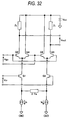
- FIG. 32 Conventional variable gain amplifier circuits are shown in Figs. 32 - 34 by way of example.
- the conventional variable gain amplifier circuit shown in Fig. 32 as a first example is formed with a pair of common-emitter amplifier circuits having bipolar transistors Q1 and Q2, and differential pairs of bipolar transistors Q3 and Q4 and bipolar transistors Q5 and Q6.
- an input signal Vin is fed into the bases of the bipolar transistors Q1 and Q2 and the output current of the common-emitter amplifier circuit branches out in accordance with a gain control voltage Vgc fed into the bases of the bipolar transistors Q3 - Q6 forming the differential pair.
- the voltage gain Av2 of the variable gain amplifier circuit is expressed by an equation 1 a below and controlled by the gain control voltage Vgc under the assumption of ideal bipolar transistors.
- Av2 gm2 ⁇ ZL ⁇ exp(Vgc/Vt)/(exp(Vgc/Vt) + 1) provided gm2 is expressed by an equation 1 b below:
- gm2 1/(Vt/IO) + (Re)) where Vt is thermal voltage (about 26 mV at room temperature (see Non-Patent Document 1, for example).
- the conventional variable gain amplifier circuit shown in Fig. 33 as a second example employs bipolar transistors Q3 and Q4 as constant current sources and controls the gain of a set of common-emitter amplifier circuits having bipolar transistors Q1 and Q2 by varying a collector current IO in accordance with the gain control voltage Vgc.
- the voltage gain Av3 of the variable gain amplifier circuit is expressed by an equation 2a below and controlled by the gain control voltage Vgc under the assumption of ideal bipolar transistors.
- Is denotes the saturation currents of the bipolar transistors Q3 and Q4, and log () a natural logarithmic function (see Patent Document 1, for example).
- variable gain amplifier circuit shown in Fig. 34 as a third example is similar in configuration to the conventional example 2 shown in Fig. 33, wherein though a voltage gain Av4 is controlled by varying the collector current IO likewise, the way to vary the collector current IO differs.
- the voltage gain Av4 of the variable gain amplifier circuit is expressed by an equation 3a below:
- gm4 1/((Vt/IO) +(Re)) (Non-Patent Document 1) Robert G Meyer, and William D.
- Patent Document 1 JP-T-10-503917 (Fig. 1)
- Patent Document 2 JP-UM-A-1-179620 (Fig. 1)
- the conventional variable gain amplifier circuit shown in Fig. 32 as the first example always consumes a constant collector current IO irrespective of the gain control voltage Vgc as seen from Eq. 1 a and Eq. 1 b.
- ⁇ refers to an absolute value.
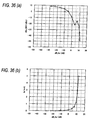
- approximation based on the approach that midpoint ground of a differential amplifier circuit is valid has been used for the sake of brevity. As a signal grows larger, the signal deviates from the approximation, whereupon the IM3 deteriorates further.
- Figs. 35(a) and (b) show the relation between the suppression ratio IM3 and the collector current IO with respect to a voltage gain Av when the voltage gain Av is controlled by varying the gain control voltage Vgc calculated from the Eqs. 1 a and 1 b and Eq. 4 (the voltage gain being Av2 in the equation).
- the suppression ratio IM3 and the voltage gain Av are not antilogarithms but those expressed in dBc or dB as a unit. Therefore, the problem is that because the conventional variable gain amplifier circuit as the first example always consumes a relatively large current irrespective of the voltage gain, the current consumed thereby never decreases even though the voltage gain is lowered.
- the conventional variable gain amplifier circuits respectively shown in Fig. 33 and Fig. 34 as the second and third examples reveal that as seen from Eqs. 2a and 2b and Eqs. 3a and 3b, the collector current decreases when the voltage gain is lowered.
- An object of the invention made to solve the foregoing problems is to provide an excellent variable gain amplifier circuit which causes an electric current to decrease when a voltage gain is lowered and is substantially free of a deterioration in distortion characteristics represented by the suppression ratio, and a radio communication apparatus using the same.
- a variable gain amplifier circuit is provided with a plurality of common-emitter amplifier circuits which are different in voltage gain and employ bipolar transistors and switch means for selecting the plurality of amplifier circuits, wherein: the bases of the bipolar transistors are connected in common with each other; and the switch means are connected to the respective emitter sides of the bipolar transistors.
- the current decreases when the voltage gain is lowered and a deterioration in distortion characteristics represented by the suppression ratio can substantially be obviated.
- a variable gain amplifier circuit is provided with a plurality of amplifier circuits which are different in voltage gain and employ bipolar transistors and formed with an common-emitter and common-base cascade connection and switch means for selecting the plurality of amplifier circuits, wherein: the bases of the common-emitter bipolar transistors are connected in common with each other; and the switch means are connected to the respective emitter sides of the bipolar transistors.
- the current decreases when the voltage gain is lowered and it is possible to achieve the effect of enlarging the dynamic range of gain control in addition to the effect of substantially obviating a deterioration in distortion characteristics represented by the suppression ratio.
- a collector current ratio between the plurality of amplifier circuits is inversely proportional to an emitter degeneration resistance ratio.
- an emitter area ratio between common-emitter transistors in the plurality of amplifier circuits is inversely proportional to the emitter degeneration resistance ratio.
- the emitter area ratio inversely proportional to the emitter degeneration resistance ratio, that is, making the emitter area ratio equal to the ratio of the reciprocal of the emitter degeneration resistance whereby to selectively switch the plurality of amplifier circuits different in voltage gain with the switch means.
- the emitter area ratio between the common-emitter transistors in the plurality of amplifier circuits is in powers of 2.
- the area ratio is readily attainable with accuracy when the physical configuration of the element is taken into consideration.
- the variable gain amplifier circuit as IC or LSI, for example, two of the bipolar transistors having the same configuration are connected in parallel, whereby the emitter area can be doubled with accuracy.
- the emitter degeneration resistance ratio between the plurality of amplifier circuits is in powers of 2.
- the emitter degeneration resistance ratio is readily attainable with accuracy when the physical configuration of the element is taken into consideration.
- the variable gain amplifier circuit as IC or LSI, for example, two of the resistance elements having the same configuration are connected in parallel, whereby the resistance value can be halved with accuracy.
- a variable gain amplifier circuit is provided with a plurality of common-source amplifier circuits which are different in voltage gain and employ field effect transistors and switch means for selecting the plurality of amplifier circuits, wherein: the gates of the field effect transistors are connected in common with each other; and the switch means are connected to the respective source sides of the field effect transistors.
- the circuit can be operated with a lower supply voltage by employing the field effect transistors.
- a variable gain amplifier circuit is provided with a plurality of amplifier circuits which are different in voltage gain and employ field effect transistors and formed with a common-source and common-gate cascade connection and switch means for selecting the plurality of amplifier circuits, wherein: the gates of the common-source field effect transistors are connected in common with each other; and the switch means are connected to the respective source sides of the field effect transistors.
- the current decreases when the voltage gain is lowered and it is possible to achieve the effect of enlarging the dynamic range of gain control in addition to the effect of substantially obviating a deterioration in distortion characteristics represented by the suppression ratio.
- the circuit can be operated with a lower supply voltage by employing the field effect transistors.
- a drain current ratio between the plurality of amplifier circuits is inversely proportional to a source degeneration resistance ratio.
- a gate width ratio between common-source transistors in the plurality of amplifier circuits is inversely proportional to the source degeneration resistance ratio.
- the gate width ratio between the common-source transistors in the plurality of amplifier circuits is in powers of 2.
- the gate width ratio is readily attainable with accuracy when the physical configuration of the element is taken into consideration.
- the variable gain amplifier circuit as IC or LSI, for example, two of the MOS transistors having the same configuration are connected in parallel, whereby the gate width can be doubled with accuracy.
- the source degeneration resistance ratio between the plurality of amplifier circuits is in powers of 2.
- the source degeneration resistance ratio is readily attainable with accuracy when the physical configuration of the element is taken into consideration.
- the variable gain amplifier circuit as IC or LSI, for example, two of the resistance elements having the same configuration are connected in parallel, whereby the resistance value can be halved with accuracy.
- the switch means is a current source.
- the plurality of amplifier circuits can be selected so as to control the voltage gain by setting the collector current or the drain current in each of the plurality of amplifier circuits with the current source, the current decreases when the voltage gain is lowered and a deterioration in distortion characteristics can substantially be obviated.
- the switch means is a transistor.
- the transistor switch means when the plurality of amplifier circuits different in voltage gain are selected by the transistor switch means, switching these amplifier circuits is made such that the emitter or source side of an amplifier circuit to be selected is held at the ground potential, whereas the emitter or source side of what is not to be selected is opened, so that the voltage gain becomes controllable.
- the current decreases when the voltage gain is lowered and a deterioration in distortion characteristics can substantially be obviated.
- the on-resistance of the transistor is minimized or the on-resistance ratio is set equal to the emitter degeneration resistance ratio or the source degeneration resistance ratio, whereby the voltage gain is made controllable with accuracy.
- a circuit can easily be integrated into LSI by using transistors.
- the switch means is an inverter.
- the inverter switch means when the plurality of amplifier circuits different in voltage gain are selected by the inverter switch means, switching these amplifier circuits is made such that the emitter or source side of an amplifier circuit not to be selected is held at a positive power supply voltage, so that the voltage gain becomes controllable.
- the current decreases when the voltage gain is lowered and a deterioration in distortion characteristics can substantially be obviated.
- a circuit can easily be integrated into LSI by using inverter.
- variable gain amplifier circuits Any one of the variable gain amplifier circuits above has bias circuits respectively corresponding to the plurality of amplifier circuits.
- the collector or drain current ratio can accurately be realized by providing the bias circuits when the voltage gain is controlled.
- variable gain amplifier circuits has a decoder as decoding means for receiving and decoding a digital signal and selecting any one of the plurality of amplifier circuits by its output corresponding to the digital signal received.
- the voltage gain of the variable gain amplifier circuit is made controllable by using the decoder in every unit of predetermined quantities, depending on the value of an input signal to the decoder.
- variable gain amplifier circuits has a decoder as decoding means for receiving and decoding a digital signal and selecting any combination of amplifier circuits by its output corresponding to the digital signal received.
- the voltage gain of the variable gain amplifier circuit is made controllable by using the decoder in each smaller predetermined unit over a predetermined range depending on the input signal value to the decoder.
- variable gain amplifier circuits has decoding means for receiving and decoding a digital signal, including a first decoder for selecting one of the plurality of amplifier circuits by its output corresponding to the digital signal received and a second decoder for selecting any combination of amplifier circuits by its output corresponding to the digital signal received.
- variable gain amplifier circuit using the first decoder and the variable gain amplifier circuit using the second decoder are connected in series, for example, whereby the voltage gains of the variable gain amplifier circuits become controllable in each smaller predetermined unit over a predetermined range depending on the input signal value to the decoder.
- radio communication apparatus having any one of the variable gain amplifier circuits above as an amplifier circuit is provided by the invention.
- variable gain amplifier circuit bodies denote variable gain amplifier circuit bodies; 12, 22, decoders; 104, a transmission RF variable gain amplifier circuit; 107, a reception RF variable gain amplifier circuit; Q1 - Q6 and Qb1 - Qb6, bipolar transistors; Mn0 - Mn2, Mp0 - Mp2, Mp20 - Mp22, Mp200 and M1 - M8, MOS transistors; Re, and Re0 - Re2, emitter degeneration resistors; Rec0 - Rec2, emitter degeneration resistors in phase; Rs0 - Rs2, source degeneration resistors; Rsc0 - Rsc2, source degeneration resistors in phase; SW0, SW1 and SW2, switches; Ic10 and 10, collector currents; and gain_state_1 and gain_state_2, digital signals.
- Fig. 1 is a circuit diagram showing a variable gain amplifier circuit according to a first embodiment of the invention.
- the variable gain amplifier circuit according to the first embodiment of the invention is formed such that the bases of bipolar transistors Q1, Q3 and Q5 and the bases of bipolar transistors Q2, Q4 and Q6 are connected in common with each other, these bipolar transistors forming a plurality of common-emitter amplifier circuits; a switch SW2 is connected to the emitter sides of the bipolar transistors Q1 and Q2; a switch SW1 to the emitter sides of bipolar transistors Q3 and Q4; and a switch SW0 to the emitter sides of the bipolar transistors Q5 and Q6.
- the desired common-emitter amplifier circuit can be selected by each of the switches SW2, SW1 and SW0.
- the emitter area ratio between the bipolar transistors forming the common-emitter amplifier circuit is in powers of 2 and the resistance value ratio between the emitter degeneration resistors Re0, Re1 and Re2 is inversely proportional to the emitter area ratio between the bipolar transistors.
- the reason for setting the emitter area ratio between the bipolar transistors in powers of 2 is that the area ratio is readily realizable with accuracy when the physical configuration of the element is taken into consideration.
- the circuit according to this embodiment of the invention as IC or LSI, for example, two of the resistance elements or bipolar transistors having the same configuration are connected in parallel, whereby the resistance value of each resistance element can accurately be halved or the emitter area of each can accurately be doubled.
- the emitter degeneration resistance ratio is so arranged as to be preferably in powers of 2. Even though the area ratio of the bipolar transistor is not set to powers of 2 but to any given ratio, the same circuit operation is made possible thereby, provided the ratio of the emitter degeneration resistance value is inversely proportional to the emitter area ratio of the bipolar transistor.
- the ratio of a collector current IO is also in powers of 2.
- the collector current ratio in the amplifier circuit by mean of the bipolar transistor becomes inversely proportional to the emitter degeneration resistance ratio.
- the gain_state is defined as being 0, 1 or 2.
- the voltage gain Av1 of the variable gain amplifier circuit according to the first embodiment of the invention is made controllable according to the gain_state as expressed by an equation 7a below under the assumption of ideal bipolar transistors.
- Av1 gm1 ⁇ ZL provided gm1
- Re and IO are expressed by equations 7b, 7c and 7d below.
- gm1 1/(Re + (Vt/IO)
- Re Re5/(2 gain_state )
- IO Ic10 ⁇ (2 gain_state ) wherein 2 gain_state denotes 2 to the power of gain_state; and 1c10 denotes the collector current IO when the gain_state is 0.
- the bias voltages of the bases of the bipolar transistors Q1 and Q2 are set constant for the sake of brevity as described above, the bias voltages of the bases are not necessarily constant in that similar gain control is made possible by devising an alternative bias circuit so that the collector current 10 is changed in a manner inversely proportional to the emitter resistant Re.
- Fig. 2 is a circuit diagram showing a variable gain amplifier circuit configuration including bias circuits for exactly realizing the ratio of the collector current IO above as an application example of the first embodiment of the invention.
- variable gain amplifier circuit as the application example is provided with bias circuits respectively corresponding to a plurality of common-emitter amplifier circuits, whereby the ratio of the collector current IO becomes exactly attainable even though the collector current IO is changed by the gain_state.
- the collector current decreases when the voltage gain is lowered in this variable gain amplifier circuit.
- a suppression ratio IM3 becomes equal to what results from Eq. 3 and Eq. 4 and is expressed by an equation 8 below under the assumption of ideal bipolar transistors.
- IM3 (3/4) ⁇
- FIGs. 3(a) and (b) show the relation between the suppression ratio IM3 and the collector current 10 with respect to a voltage gain Av when the voltage gain Av is controlled by varying the gain_state calculated from the Eqs. 7a - 7d (the voltage gain being Av1 in the equations).
- the bases of the bipolar transistor pairs forming the plurality of common-emitter amplifier circuits are set for common use and the switches are provided on the respective emitter sides of the bipolar transistor pairs forming the common-emitter amplifier circuits whereby to use the switch for selecting any one of the common-emitter amplifier circuits.
- the current decreases when the voltage gain is lowered, so that a variable gain amplifier circuit substantially free of a deterioration in distortion characteristics can be realized.
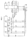
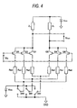
- Fig. 4 is a circuit diagram showing a variable gain amplifier circuit configuration as a modified example of the first embodiment of the invention.
- a positive power supply voltage Vcc is usable without holding the emitter side of the bipolar transistor at the ground potential gnd by switching the switches SW2, SW1 and SW0.
- Fig. 5 is a circuit diagram showing a variable gain amplifier circuit configuration according to a second embodiment of the invention.
- variable gain amplifier circuit is such that the differential type circuit in the differential form shown in Fig. 1 according to the first embodiment of the invention is changed to a single-ended type one.
- This variable gain amplifier circuit is formed such that the bases of bipolar transistors Q1, Q3 and Q5 forming a plurality of common-emitter amplifier circuits are connected in common with each other and that switches SW2, SW1 and SW0 are connected to the respective emitter sides thereof.
- the circuit operation is the same as what is described in the first embodiment of the invention.
- the bipolar transistor When the emitter side of any bipolar transistor is held at the ground potential gnd in the configuration of Fig. 5 by switching the switches SW2, SW1 and SW0, the bipolar transistor operates as an common-emitter amplifier circuit and does not operate as the amplifier circuit when the emitter side thereof is not held at the ground potential gnd because no collector current flows.
- the voltage gain is made controllable by switching the switches SW2, SW1 and SW0 to select any one the amplifier circuits different in the voltage gain.
- the bases of the bipolar transistor forming the plurality of common-emitter amplifier circuits are connected in common with each other and the switches are provided on the respective emitter sides of the bipolar transistor forming the common-emitter amplifier circuits whereby to use the switch for selecting any one of the common-emitter amplifier circuits.
- the current decreases when the voltage gain is lowered, so that a variable gain amplifier circuit substantially free of a deterioration in distortion characteristics can be realized.
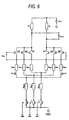
- Fig. 6 is a circuit diagram showing a variable gain amplifier circuit configuration according to a third embodiment of the invention.
- the third embodiment of the invention refers to a partially modified example of the first embodiment of the invention above.
- the difference in configuration between the third embodiment of the invention and the first embodiment thereof is that emitter degeneration resistors Rec0, Rec1 and Rec2 in phase are added to the respective bipolar transistor pairs; the rest is configured as in the first embodiment thereof.
- the resistance value ratio of each of the emitter degeneration resistors Rec0, Rec1 and Rec2 in phase is set inversely proportional to the emitter area ratio like the emitter degeneration resistors Re0, Re1 and Re2 so as to satisfy the relation of an equation 6c below.
- the collector current ratio can thus be kept constant.
- the voltage gain of the in-phase signal is made reducible by adding the emitter degeneration resistors Rec0, Rec1 and Rec2 in phase, the effect of reinforcing resistance to noise from the outside becomes newly achievable.
- the relation between the voltage gain of the differential signal, the collector current and the suppression ratio is the same as that in the first embodiment of the invention, so that the same effect still becomes achievable thereby.
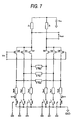
- Fig. 7 is a circuit diagram showing a modified example of the third embodiment of the invention; an emitter degeneration resistor connecting configuration is different in this modified example thereof.
- this modified example is considered to be an amplifier circuit similar to the variable gain amplifier circuit of Fig. 6, so that the same effect is also made achievable by this modified example.
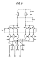
- Figs. 8 and 9 are circuit diagrams showing variable gain amplifier circuit configurations according to a fourth embodiment of the invention.
- the fourth embodiment of the invention refers to partially modified examples of the first embodiment of the invention above.
- the difference in configuration between the fourth embodiment of the invention and the first embodiment thereof is that current sources 41, 42 and 43 are used as switches; the rest is configured as in the first embodiment thereof.
- the examples shown in Figs. 8 and 9 are different in the arrangement for connecting the emitter degeneration resistors Re0, Re1 and Re2 and the current sources 41, 42 and 43.
- the collector current ratio set at each of the current sources 41, 42 and 43 is set by Eq. 7d likewise in the variable gain amplifier circuit according to the fourth embodiment of the invention, the relation between the voltage gain, the collector current and the suppression ratio is the same as that in the first embodiment of the invention, so that the same effect becomes achievable thereby.
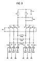
- Fig. 10 is a circuit diagram showing a variable gain amplifier circuit configuration according to a fifth embodiment of the invention.
- the fifth embodiment of the invention refers to a partially modified example of the first embodiment of the invention above.
- the difference in configuration between the fifth embodiment of the invention and the first embodiment thereof is that MOS transistors Mn0, Mn1 and Mn2 are used as switches; the rest is configured as in the first embodiment thereof.
- MOS transistors Mn0, Mn1 and Mn2 are used as switches; the rest is configured as in the first embodiment thereof.
- the relation between the voltage gain, the collector current and the suppression ratio is the same as that in the first embodiment of the invention, so that the same effect becomes achievable thereby.
- the voltage gain is made controllable more precisely by making the gate width as large as possible to make the on-resistance as small as possible or making the on-resistance ratio equal to the emitter degeneration resistance ratio.
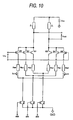
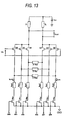
- Figs. 11 - 13 are circuit diagrams showing variable gain amplifier circuit configurations as modified examples of the fifth embodiment of the invention.
- the MOS transistors are alternatively employed as switches in a manner corresponding to the arrangements made according to the second and third embodiments of the invention as shown in Figs. 5 - 7, whereupon the same effect is also achievable by each of the modified examples above.
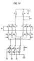
- Fig. 14 is a circuit diagram showing a variable gain amplifier circuit configuration according to a sixth embodiment of the invention.
- the sixth embodiment of the invention refers to a partially modified example of the fifth embodiment of the invention above.
- MOS inverters formed with MOS transistors Mn0, Mn1, Mn2, Mp0, Mp1 and Mp2 are used as switches so that when no common-emitter amplifier circuit is selected, the emitter side of the bipolar transistor is not opened but held at the potential of the positive power supply voltage; the rest is configured as in the first embodiment thereof.
- the bipolar transistor When the bipolar transistor is saturated by holding the emitter side of the bipolar transistor at the potential of the positive power supply voltage, it ceases to operate as an amplifier circuit, so that the same gain control as that in the first and fifth embodiments of the invention is performable. Consequently, even in this variable gain amplifier circuit configuration according to the fifth embodiment of the invention, the relation between the voltage gain, the collector current and the suppression ratio is the same as that in the first and fifth embodiments of the invention, so that the same effect becomes achievable thereby.
- the voltage gain is made controllable more precisely by making the gate width as large as possible to make the on-resistance as small as possible or making the on-resistance ratio equal to the emitter degeneration resistance ratio.
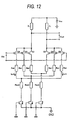
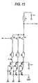
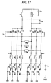
- Figs. 15 - 17 are circuit diagrams showing variable gain amplifier circuit configurations as modified examples of the sixth embodiment of the invention.
- the MOS inverters are alternatively employed as switches in a manner corresponding to the arrangements made according to the second and third embodiments of the invention as shown in Figs. 5 - 7, whereupon the same effect is also achievable by each of the modified examples above.
- the MOS inverters are employed as inverters by way of example, it is possible to have the same operation performed by using inverters different in configuration and the same effect is also achievable then.
- Fig. 18 is a circuit diagram showing a variable gain amplifier circuit configuration according to a seventh embodiment of the invention.
- the seventh embodiment of the invention refers to a partially modified example of the first embodiment of the invention above.
- the difference in configuration between the seventh embodiment of the invention and the first embodiment thereof is that common-base bipolar transistors Q7 and Q8 are added with an common-emitter and common-base cascade connection; the rest is configured as in the first embodiment thereof.
- a parasitic capacitance between the input Vin and the output Vout grows greater because a capacitance Cjc between the bases and collectors of the bipolar transistors Q1 and Q2 works directly according to the first embodiment of the invention, whereas the parasitic capacitance between the input Vin and the output Vout can be reduced by adding the common-base bipolar transistors Q7 and Q8.
- the operation of the circuit is basically the same as that in the first embodiment of the invention and the voltage gain Av and the suppression ratio IM3 are equal to Eqs. 7a - 7d and Eq. 8 under the assumption of ideal bipolar transistors.
- the voltage gain can be controlled according to Eqs. 7a - 7d in an ideal case where the parasitic capacitance can be disregarded in the variable gain amplifier circuit according to any embodiment of the invention.
- the dynamic range of the gain control can be enlarged.
- variable gain amplifier circuit is arranged with the common-emitter and common-base cascade connection according to the seventh embodiment of the invention whereby to make achievable the effect of enlarging the dynamic range of the gain control, in addition to the effect of the first embodiment thereof.
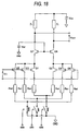
- Fig. 19 is a circuit diagram showing a variable gain amplifier circuit configuration as a first modified example of the seventh embodiment of the invention.
- This modified example refers to the variable gain amplifier circuit having the common-emitter and common-base cascade connection in a manner corresponding to the arrangement made according to the modified example of the sixth embodiment of the invention as shown in Fig. 16, whereupon the same effect is also achievable thereby.
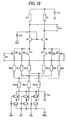
- Fig. 20 is a circuit diagram showing a variable gain amplifier circuit configuration as a second modified example of the seventh embodiment of the invention.
- This modified example corresponds to the configuration of the modified example according to the first embodiment of the invention as shown in Fig. 4 in that the emitter sides of the bipolar transistors are held at the ground potential gnd by switching the switches SW2, SW1 and SW0 and moreover held at the positive power supply voltage Vcc when not held at the ground potential gnd.
- the same effect is also achievable.
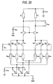
- Fig. 21 is a circuit diagram showing a variable gain amplifier circuit configuration according to an eighth embodiment of the invention.
- the eighth embodiment of the invention refers to a partially modified example of the first embodiment of the invention above.
- the difference in configuration between the eighth embodiment of the invention and the first embodiment thereof is that MOS transistors in place of bipolar transistors are employed.
- the variable gain amplifier circuit in this case is formed such that the gates of MOS transistors M1, M3 and M5 and the gates of MOS transistors M2, M4 and M6 are connected in common with each other, these MOS transistors forming a plurality of common-source amplifier circuits; a switch SW2 is connected to the source sides of the MOS transistors M1 and M2; a switch SW1 to the source sides of MOS transistors M3 and M4; and a switch SW0 to the source sides of the MOS transistors M5 and M6.
- the ratio of each of the resistance values Rs0, Rs1 and Rs2 of the source degeneration resistors in the plurality of common-source amplifier circuits is set inversely proportional to the ratio of the gate width of the MOS transistor.
- the ratio of the gate width of each MOS transistor and the ratio of the resistance value of the source degeneration resistor are in powers of 2.
- the drain current ratio is set inversely proportional to the source degeneration resistance ratio in the plurality of common-source amplifier circuits.
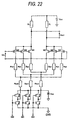
- FIG. 22 is a circuit diagram showing a variable gain amplifier circuit configuration as a modified example of the eighth embodiment of the invention. This modified example is so configured as to employ the MOS transistors in place of the bipolar transistors in a manner corresponding to the configuration of the modified example according to the sixth embodiment of the invention as shown in Fig. 16 and the same effect is also achievable.
- MOS transistors as field effect transistors according to this embodiment of the invention
- elements for use are not limited to MOS transistors but include other field effect transistors such as GaAs MESFETs using compound semiconductors with the same effect achievable.
- Figs. 23 and 24 are circuit diagrams showing variable gain amplifier circuits according to a ninth embodiment of the invention.
- the ninth embodiment of the invention refers to partially modified examples of the seventh embodiment thereof.
- the difference in configuration between the ninth embodiment of the invention and the seventh embodiment thereof is that MOS transistors in place of bipolar transistors are employed.
- the common-gate MOS transistors like M7 and M8 are added to the configuration according to the eighth embodiment of the invention so that an amplifier circuit having a common-source and common-gate cascade connection is formed.
- the arrangement according to the ninth embodiment thereof makes achievable the effect of operating the circuit with a lower power supply voltage, in addition to the effect of the seventh embodiment thereof.
- MOS transistors as field effect transistors according to this embodiment of the invention
- elements for use are not limited to MOS transistors but include other field effect transistors such as GaAs MESFETs using compound semiconductors with the same effect achievable.
- Fig. 25 is a block diagram showing a variable gain amplifier circuit configuration according to a tenth embodiment of the invention.
- variable gain amplifier circuit is formed with the variable gain amplifier circuit referred to in the first - ninth embodiments thereof as a variable gain amplifier circuit body (VGA1) 11, and a decoder (DECODER 1) 12 as an additional element.
- VGA1 variable gain amplifier circuit body
- DECODER 1 decoder
- the decoder 12 performs digital signal processing as shown in Table 1 whereby to feed '1' into any one of the inputs of SW2, SW1 and SW0 of the variable gain amplifier circuit body 11 in response to a digital signal gain_state_1 for setting the gain state and selects one of a plurality of amplifier circuits contained in the variable gain amplifier circuit body 11.
- gain_state_1 SW0 SW1 SW2 Voltage gain Av (dB) dB_Av (dBc) dBc_IM3 IO(mA) 2 0 0 1 3.623 11.182 -47.998 5.000 1 0 1 0 1.812 5.161 -47.998 2.500 0 1 0 0 0.906 -0.859 -47.998 1.250
- the method of inputting the digital signal gain_state_1 As a method of inputting the digital signal gain_state_1 according to the tenth embodiment of the invention, there is a method of inputting serial data by using a clock terminal clk, a data terminal data and a strobe terminal stb.
- the method of inputting the digital signal gain_state_1 is not limited to the above-mentioned but may include various modified examples to be taken into consideration.
- Fig. 26 is a graph showing the relation of a voltage gain Av (displayed in dB) to a digital signal gain_state_1 corresponding to Table 1.
- the voltage gain of the variable gain amplifier circuit is made controllable by using the decoder in every unit of predetermined quantities, for example, about 6 dB depending on the value of an input signal to the decoder.
- the gain control range may be enlarged further by increasing the number of bits.
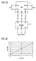
- Fig. 27 is a block diagram showing a variable gain amplifier circuit configuration according to an eleventh embodiment of the invention.
- variable gain amplifier circuit is formed with the variable gain amplifier circuit referred to in the first - ninth embodiments thereof as a variable gain amplifier circuit body (VGA2) 21, and a decoder circuit (DECODER 2) 22 as an additional element.
- VGA2 variable gain amplifier circuit body
- DECODER 2 decoder circuit
- the decoder 22 always feeds '1' into SW2 corresponding to an amplifier circuit having the largest voltage gain within the variable gain amplifier circuit body 21 and performs digital signal processing as shown in Table 2 by receiving a digital signal gain_state_2 for setting the gain state whereby to feed '1' or '2' into the input of each of SW0 and SW1 of the variable gain amplifier circuit body 22 in order to select any combination of amplifier circuits out of those corresponding to SW0 and SW1.
- the method of inputting the digital signal gain_state_2 there is a method of inputting serial data by using a clock terminal clk, a data terminal data and a strobe terminal stb.
- the method of inputting the digital signal gain_state_2 is not limited to the above-mentioned but may include various modified examples to be taken into consideration.
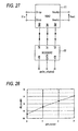
- Fig. 28 is a graph showing the relation of a voltage gain Av (displayed in dB) to a digital signal gain_state_2 corresponding to Table 2.
- the voltage gain of the variable gain amplifier circuit is made controllable by using the decoder in each smaller predetermined unit over a predetermined range of 6 dB, for example, depending on the input signal value to the decoder.
- the voltage gain control unit may be made smaller by increasing the number of bits.
- the setting of gain control of the whole variable gain amplifier circuit body 21 can by changed by changing the setting of the voltage gain of the amplifier circuit into which '1' is always fed.
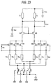
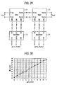
- Fig. 29 is a block diagram showing a variable gain amplifier circuit configuration according to a twelfth embodiment of the invention.
- variable gain amplifier circuit is formed by connecting the variable gain amplifier circuit described in the tenth embodiment thereof and the variable gain amplifier circuit described in the eleventh embodiment thereof in series.
- the voltage gain becomes the product (the sum displayed in dB) of the voltage gains of both variable gain amplifier circuits.
- the voltage gain is regarded as being controllable by the gain_state_3 when the combination of the digital signal gain_state_1 and digital signal gain_state_2 is defined as the gain_state_3.
- Fig. 30 is a graph showing the relation of the voltage gain Av (displayed in dB) to the digital signal gain_state_3 corresponding to Table 3.
- variable gain amplifier circuits using the decoders are connected in series, whereby the voltage gains of the variable gain amplifier circuits become controllable in each smaller predetermined unit over a predetermined range depending on the input signal value to the decoder.
- a 3-bit configuration is shown by way of example according to the twelfth embodiment of the invention, it is possible to not only enlarge the dynamic range of the gain control but also control the voltage gain at smaller intervals by increasing the number of bits.
- Fig. 31 is a block diagram showing the configuration of a radio communication apparatus according to a thirteenth embodiment of the invention.
- the thirteenth embodiment of the invention refers to an example of an application of the variable gain amplifier circuit according to tenth - twelfth embodiments thereof to the radio communication apparatus.
- This radio communication apparatus is equipped with an antenna 106 and a duplexer 105; its transmission system has a transmission base band signal processing unit 101, a modulator 102, a transmission oscillator 103 and a transmission RF variable gain amplifier circuit 104; and its reception system has a reception RF variable gain amplifier circuit 107, a demodulator 108, a reception oscillator 109 and a reception base band signal processing unit 110.
- Signal processing such as the encoding, amplification, band limiting processing and the like of a base band transmitting signal is performed in the transmission base band signal processing unit 101 by means of the transmission data signal received.
- Frequency conversion is conducted in the modulator 102 by mixing the local oscillating signal generated by the transmission oscillator 103 and the transmitting signal to obtain a transmission RF signal.
- gain control is then performed to adjust the transmission RF signal to a suitable signal level in order to avoid the saturation of the reception circuit in the partner station in case where the distance to a communicating partner is short or to lower interference with any other radio communication apparatus, for example, whereby the signal is radiated as an radio wave from the antenna 106 via the duplexer 105.
- a reception RF signal received by the antenna 106 is fed into the reception RF variable gain amplifier circuit 107 via the duplexer 105.
- gain control is then performed to adjust the reception RF signal to a suitable signal level in order to restrain receiving signal level fluctuation due to a change in the distance to the communication partner or to avoid the saturation of the amplifier circuit because of a high-level input signal, for example.
- frequency conversion is conducted by mixing the local oscillating signal generated by the reception oscillator 109 and a reception RF signal in the demodulator 108 to obtain a base band receiving signal.
- Signal processing such as the band limiting processing, amplification, decoding and the like of the receiving signal is performed in the reception base band signal processing unit 110 to regenerate the original data signal received from the communication partner, whereby the signal is outputted as a reception data signal.
- variable gain amplifier circuit described according to the tenth - twelfth embodiments thereof is used for at least one of the transmission RF variable gain amplifier circuit 104 and reception RF variable gain amplifier circuit 107.
- the current decreases when the voltage gain is lowered, so that a radio communication apparatus substantially free of a deterioration in distortion characteristics can be realized.
- the bases of the bipolar transistor or the sources of the MOS transistors forming the plurality of common-emitter amplifier circuits are set for common use and the switches are provided on the respective emitter sides of the bipolar transistors or the respective source sides of MOS transistors whereby to use the switch for selecting any one of the common-emitter amplifier circuits.
- the current decreases when the voltage gain is lowered, which results in realizing a variable gain amplifier circuit having an beautiful effect in that the amplifier circuit is substantially free of a deterioration in distortion characteristics.
- variable gain amplifier circuit substantially free of a deterioration in distortion characteristics represented by the suppression ratio as the current decreases when the voltage gain is lowered, and a radio communication apparatus equipped with the variable gain amplifier circuit.
Landscapes
- Control Of Amplification And Gain Control (AREA)
- Amplifiers (AREA)
Applications Claiming Priority (3)
| Application Number | Priority Date | Filing Date | Title |
|---|---|---|---|
| JP2003006171A JP2004266309A (ja) | 2003-01-14 | 2003-01-14 | 可変利得増幅回路及び無線通信装置 |
| JP2003006171 | 2003-01-14 | ||
| PCT/JP2004/000181 WO2004064251A1 (ja) | 2003-01-14 | 2004-01-14 | 可変利得増幅回路及び無線機 |
Publications (1)
| Publication Number | Publication Date |
|---|---|
| EP1560331A1 true EP1560331A1 (de) | 2005-08-03 |
Family
ID=32709051
Family Applications (1)
| Application Number | Title | Priority Date | Filing Date |
|---|---|---|---|
| EP04702042A Withdrawn EP1560331A1 (de) | 2003-01-14 | 2004-01-14 | VERSTûRKERSCHALTUNG MIT VARIABLER VERSTûRKUNG UND FUNKMASCHINE |
Country Status (4)
| Country | Link |
|---|---|
| US (1) | US20060022748A1 (de) |
| EP (1) | EP1560331A1 (de) |
| JP (1) | JP2004266309A (de) |
| WO (1) | WO2004064251A1 (de) |
Cited By (5)
| Publication number | Priority date | Publication date | Assignee | Title |
|---|---|---|---|---|
| US7180310B2 (en) | 2004-10-27 | 2007-02-20 | Advantest Corporation | Amplitude varying driver circuit and test apparatus |
| CN101826843A (zh) * | 2010-05-06 | 2010-09-08 | 复旦大学 | 一种在低增益时线性度优化的可变增益放大器 |
| CN101375504B (zh) * | 2006-01-24 | 2011-05-18 | 英国福威科技有限公司 | 低噪声放大器 |
| CN102354240A (zh) * | 2011-07-25 | 2012-02-15 | 复旦大学 | 一种可拓展高频带宽的电路结构 |
| US10693231B2 (en) | 2017-09-11 | 2020-06-23 | Qualcomm Incorporated | Transmit/receive switching circuit |
Families Citing this family (18)
| Publication number | Priority date | Publication date | Assignee | Title |
|---|---|---|---|---|
| DE102004039830B4 (de) * | 2004-08-17 | 2007-11-08 | Infineon Technologies Ag | Verstärkerschaltung mit einstellbarer wertdiskreter Verstärkung, Verwendung der Verstärkerschaltung und Verfahren zum Betreiben eines wertdiskret einstellbaren Verstärkers |
| JP2007074121A (ja) * | 2005-09-05 | 2007-03-22 | Fujitsu Ltd | 増幅器及び相互コンダクタンス制御方法 |
| JP2007104141A (ja) * | 2005-09-30 | 2007-04-19 | Mitsumi Electric Co Ltd | 可変利得回路 |
| JP2008141358A (ja) * | 2006-11-30 | 2008-06-19 | Mitsumi Electric Co Ltd | 利得可変増幅回路 |
| JP2009088582A (ja) * | 2007-09-27 | 2009-04-23 | Tdk Corp | 増幅回路及びこれを備える光ピックアップ |
| JP5215676B2 (ja) * | 2008-01-16 | 2013-06-19 | シャープ株式会社 | 可変利得増幅器 |
| JP5239904B2 (ja) * | 2009-01-28 | 2013-07-17 | 横河電機株式会社 | 差動増幅器 |
| JP5287439B2 (ja) * | 2009-04-01 | 2013-09-11 | 日本電気株式会社 | 電圧電流変換利得制御器、電圧電流変換利得制御方法及び無線装置 |
| JP5308243B2 (ja) * | 2009-06-10 | 2013-10-09 | 株式会社日立製作所 | 可変ゲイン回路 |
| JP5315307B2 (ja) * | 2010-08-24 | 2013-10-16 | 株式会社日立製作所 | エレベーター装置 |
| US8797098B2 (en) | 2012-05-22 | 2014-08-05 | Fujitsu Limited | Variable gain amplifier |
| JP6359928B2 (ja) * | 2014-09-26 | 2018-07-18 | 日本電信電話株式会社 | ドライバ回路 |
| DE112017001304T5 (de) * | 2016-03-14 | 2018-11-22 | Analog Devices, Inc. | Aktive Linearisierung für Breitbandverstärker |
| US10389312B2 (en) | 2017-01-26 | 2019-08-20 | Analog Devices, Inc. | Bias modulation active linearization for broadband amplifiers |
| US10848109B2 (en) | 2017-01-26 | 2020-11-24 | Analog Devices, Inc. | Bias modulation active linearization for broadband amplifiers |
| TWI672903B (zh) | 2018-10-03 | 2019-09-21 | 立積電子股份有限公司 | 放大器電路 |
| US12040757B2 (en) | 2018-10-03 | 2024-07-16 | Richwave Technology Corp. | Amplifier circuit |
| JP7514505B2 (ja) * | 2020-03-19 | 2024-07-11 | ザインエレクトロニクス株式会社 | 増幅装置 |
Family Cites Families (9)
| Publication number | Priority date | Publication date | Assignee | Title |
|---|---|---|---|---|
| US3737797A (en) * | 1971-03-26 | 1973-06-05 | Rca Corp | Differential amplifier |
| JPS60212013A (ja) * | 1984-04-05 | 1985-10-24 | Nec Corp | 多段増幅器 |
| JP3322600B2 (ja) * | 1997-03-31 | 2002-09-09 | 三洋電機株式会社 | 電流調整回路 |
| JPH1127068A (ja) * | 1997-06-30 | 1999-01-29 | Nec Ic Microcomput Syst Ltd | 利得制御増幅器及びその制御方法 |
| JPH11177357A (ja) * | 1997-12-10 | 1999-07-02 | Fujitsu Ltd | 利得可変増幅回路 |
| US5999044A (en) * | 1998-04-13 | 1999-12-07 | Credence Systems Corporation | Differential driver having multiple output voltage ranges |
| JP3664010B2 (ja) * | 1999-12-10 | 2005-06-22 | 岩崎通信機株式会社 | アナログ・スイッチ回路 |
| JP3585853B2 (ja) * | 2001-02-23 | 2004-11-04 | シャープ株式会社 | 可変利得増幅器 |
| JP3970623B2 (ja) * | 2001-02-28 | 2007-09-05 | シャープ株式会社 | 可変利得増幅器 |
-
2003
- 2003-01-14 JP JP2003006171A patent/JP2004266309A/ja active Pending
-
2004
- 2004-01-14 WO PCT/JP2004/000181 patent/WO2004064251A1/ja not_active Ceased
- 2004-01-14 US US10/530,993 patent/US20060022748A1/en not_active Abandoned
- 2004-01-14 EP EP04702042A patent/EP1560331A1/de not_active Withdrawn
Non-Patent Citations (1)
| Title |
|---|
| See references of WO2004064251A1 * |
Cited By (7)
| Publication number | Priority date | Publication date | Assignee | Title |
|---|---|---|---|---|
| US7180310B2 (en) | 2004-10-27 | 2007-02-20 | Advantest Corporation | Amplitude varying driver circuit and test apparatus |
| CN101375504B (zh) * | 2006-01-24 | 2011-05-18 | 英国福威科技有限公司 | 低噪声放大器 |
| US8203388B2 (en) | 2006-01-24 | 2012-06-19 | Future Waves Uk Limited | Low noise amplifier |
| CN101826843A (zh) * | 2010-05-06 | 2010-09-08 | 复旦大学 | 一种在低增益时线性度优化的可变增益放大器 |
| CN102354240A (zh) * | 2011-07-25 | 2012-02-15 | 复旦大学 | 一种可拓展高频带宽的电路结构 |
| US10693231B2 (en) | 2017-09-11 | 2020-06-23 | Qualcomm Incorporated | Transmit/receive switching circuit |
| US10910714B2 (en) | 2017-09-11 | 2021-02-02 | Qualcomm Incorporated | Configurable power combiner and splitter |
Also Published As
| Publication number | Publication date |
|---|---|
| JP2004266309A (ja) | 2004-09-24 |
| WO2004064251A1 (ja) | 2004-07-29 |
| US20060022748A1 (en) | 2006-02-02 |
Similar Documents
| Publication | Publication Date | Title |
|---|---|---|
| EP1560331A1 (de) | VERSTûRKERSCHALTUNG MIT VARIABLER VERSTûRKUNG UND FUNKMASCHINE | |
| US7339435B2 (en) | Amplifier and device having amplifier, and mutual conductance control method | |
| US8314655B2 (en) | RF power amplifier and RF power module using the same | |
| US8190115B2 (en) | Transmission line coupled to circuits and Q-enhancement cell | |
| US7109801B2 (en) | Low gate oxide stress power amplifier | |
| JP4095398B2 (ja) | 増幅器及びこれを用いた無線通信装置 | |
| JP5979160B2 (ja) | 増幅器 | |
| US8660514B1 (en) | Multiple mode RF circuit | |
| US8280339B2 (en) | Mixer capable of detecting or controlling common mode voltage thereof | |
| US11894809B2 (en) | Transistor bias adjustment for optimization of third order intercept point in a cascode amplifier | |
| US7161406B1 (en) | Method and apparatus for providing non 2:1 Gilbert cell mixer | |
| JP2004104515A (ja) | ミキサ回路 | |
| US9059662B1 (en) | Active combiner | |
| EP1532732A2 (de) | System und verfahren zum aufbau der eingangsimpedanz einer gestapelte verstärkeranordnung | |
| KR100344928B1 (ko) | 송신회로 및 무선송신장치 | |
| US6104227A (en) | RF mixer circuit and method of operation | |
| US9520833B1 (en) | Active ring mixer | |
| US6052030A (en) | Low voltage variable gain amplifier with feedback | |
| CN115276690B (zh) | 射频接收系统和输出三阶交调点oip3校准方法 | |
| US6100763A (en) | Circuit for RF buffer and method of operation | |
| CN118104127A (zh) | 用于偏置放大器的电路和方法 | |
| JP2004040735A (ja) | 半導体集積回路及び半導体集積回路の製造方法 | |
| JP2006033664A (ja) | 可変インピーダンス素子を用いた増幅器及び無線通信装置 | |
| US7423485B2 (en) | Differential circuit with improved linearity | |
| KR100505568B1 (ko) | 믹서회로 |
Legal Events
| Date | Code | Title | Description |
|---|---|---|---|
| PUAI | Public reference made under article 153(3) epc to a published international application that has entered the european phase |
Free format text: ORIGINAL CODE: 0009012 |
|
| STAA | Information on the status of an ep patent application or granted ep patent |
Free format text: STATUS: THE APPLICATION HAS BEEN WITHDRAWN |
|
| 17P | Request for examination filed |
Effective date: 20050412 |
|
| AK | Designated contracting states |
Kind code of ref document: A1 Designated state(s): AT BE BG CH CY CZ DE DK EE ES FI FR GB GR HU IE IT LI LU MC NL PT RO SE SI SK TR |
|
| AX | Request for extension of the european patent |
Extension state: AL LT LV MK |
|
| 18W | Application withdrawn |
Effective date: 20050630 |