EP1559761B1 - Poröse filmbildende Zusammensetzung, Verfahren zur Herstellung dieser Zusammensetzung, poröser Film und Halbleiterbauelement - Google Patents
Poröse filmbildende Zusammensetzung, Verfahren zur Herstellung dieser Zusammensetzung, poröser Film und Halbleiterbauelement Download PDFInfo
- Publication number
- EP1559761B1 EP1559761B1 EP05250339A EP05250339A EP1559761B1 EP 1559761 B1 EP1559761 B1 EP 1559761B1 EP 05250339 A EP05250339 A EP 05250339A EP 05250339 A EP05250339 A EP 05250339A EP 1559761 B1 EP1559761 B1 EP 1559761B1
- Authority
- EP
- European Patent Office
- Prior art keywords
- film
- porous
- acid
- crosslinkability
- semiconductor device
- Prior art date
- Legal status (The legal status is an assumption and is not a legal conclusion. Google has not performed a legal analysis and makes no representation as to the accuracy of the status listed.)
- Expired - Lifetime
Links
Images
Classifications
-
- H—ELECTRICITY
- H10—SEMICONDUCTOR DEVICES; ELECTRIC SOLID-STATE DEVICES NOT OTHERWISE PROVIDED FOR
- H10P—GENERIC PROCESSES OR APPARATUS FOR THE MANUFACTURE OR TREATMENT OF DEVICES COVERED BY CLASS H10
- H10P14/00—Formation of materials, e.g. in the shape of layers or pillars
- H10P14/60—Formation of materials, e.g. in the shape of layers or pillars of insulating materials
- H10P14/69—Inorganic materials
- H10P14/692—Inorganic materials composed of oxides, glassy oxides or oxide-based glasses
- H10P14/6921—Inorganic materials composed of oxides, glassy oxides or oxide-based glasses containing silicon
- H10P14/6922—Inorganic materials composed of oxides, glassy oxides or oxide-based glasses containing silicon the material containing Si, O and at least one of H, N, C, F or other non-metal elements, e.g. SiOC, SiOC:H or SiONC
-
- C—CHEMISTRY; METALLURGY
- C08—ORGANIC MACROMOLECULAR COMPOUNDS; THEIR PREPARATION OR CHEMICAL WORKING-UP; COMPOSITIONS BASED THEREON
- C08G—MACROMOLECULAR COMPOUNDS OBTAINED OTHERWISE THAN BY REACTIONS ONLY INVOLVING UNSATURATED CARBON-TO-CARBON BONDS
- C08G77/00—Macromolecular compounds obtained by reactions forming a linkage containing silicon with or without sulfur, nitrogen, oxygen or carbon in the main chain of the macromolecule
- C08G77/04—Polysiloxanes
- C08G77/06—Preparatory processes
- C08G77/08—Preparatory processes characterised by the catalysts used
-
- C—CHEMISTRY; METALLURGY
- C09—DYES; PAINTS; POLISHES; NATURAL RESINS; ADHESIVES; COMPOSITIONS NOT OTHERWISE PROVIDED FOR; APPLICATIONS OF MATERIALS NOT OTHERWISE PROVIDED FOR
- C09D—COATING COMPOSITIONS, e.g. PAINTS, VARNISHES OR LACQUERS; FILLING PASTES; CHEMICAL PAINT OR INK REMOVERS; INKS; CORRECTING FLUIDS; WOODSTAINS; PASTES OR SOLIDS FOR COLOURING OR PRINTING; USE OF MATERIALS THEREFOR
- C09D183/00—Coating compositions based on macromolecular compounds obtained by reactions forming in the main chain of the macromolecule a linkage containing silicon, with or without sulfur, nitrogen, oxygen, or carbon only; Coating compositions based on derivatives of such polymers
- C09D183/02—Polysilicates
-
- C—CHEMISTRY; METALLURGY
- C09—DYES; PAINTS; POLISHES; NATURAL RESINS; ADHESIVES; COMPOSITIONS NOT OTHERWISE PROVIDED FOR; APPLICATIONS OF MATERIALS NOT OTHERWISE PROVIDED FOR
- C09D—COATING COMPOSITIONS, e.g. PAINTS, VARNISHES OR LACQUERS; FILLING PASTES; CHEMICAL PAINT OR INK REMOVERS; INKS; CORRECTING FLUIDS; WOODSTAINS; PASTES OR SOLIDS FOR COLOURING OR PRINTING; USE OF MATERIALS THEREFOR
- C09D183/00—Coating compositions based on macromolecular compounds obtained by reactions forming in the main chain of the macromolecule a linkage containing silicon, with or without sulfur, nitrogen, oxygen, or carbon only; Coating compositions based on derivatives of such polymers
- C09D183/04—Polysiloxanes
-
- H—ELECTRICITY
- H10—SEMICONDUCTOR DEVICES; ELECTRIC SOLID-STATE DEVICES NOT OTHERWISE PROVIDED FOR
- H10P—GENERIC PROCESSES OR APPARATUS FOR THE MANUFACTURE OR TREATMENT OF DEVICES COVERED BY CLASS H10
- H10P14/00—Formation of materials, e.g. in the shape of layers or pillars
- H10P14/60—Formation of materials, e.g. in the shape of layers or pillars of insulating materials
- H10P14/63—Formation of materials, e.g. in the shape of layers or pillars of insulating materials characterised by the formation processes
- H10P14/6326—Deposition processes
- H10P14/6342—Liquid deposition, e.g. spin-coating, sol-gel techniques or spray coating
-
- H—ELECTRICITY
- H10—SEMICONDUCTOR DEVICES; ELECTRIC SOLID-STATE DEVICES NOT OTHERWISE PROVIDED FOR
- H10P—GENERIC PROCESSES OR APPARATUS FOR THE MANUFACTURE OR TREATMENT OF DEVICES COVERED BY CLASS H10
- H10P14/00—Formation of materials, e.g. in the shape of layers or pillars
- H10P14/60—Formation of materials, e.g. in the shape of layers or pillars of insulating materials
- H10P14/66—Formation of materials, e.g. in the shape of layers or pillars of insulating materials characterised by the type of materials
- H10P14/665—Porous materials
-
- H—ELECTRICITY
- H10—SEMICONDUCTOR DEVICES; ELECTRIC SOLID-STATE DEVICES NOT OTHERWISE PROVIDED FOR
- H10P—GENERIC PROCESSES OR APPARATUS FOR THE MANUFACTURE OR TREATMENT OF DEVICES COVERED BY CLASS H10
- H10P14/00—Formation of materials, e.g. in the shape of layers or pillars
- H10P14/60—Formation of materials, e.g. in the shape of layers or pillars of insulating materials
- H10P14/66—Formation of materials, e.g. in the shape of layers or pillars of insulating materials characterised by the type of materials
- H10P14/668—Formation of materials, e.g. in the shape of layers or pillars of insulating materials characterised by the type of materials the materials being characterised by the deposition precursor materials
- H10P14/6681—Formation of materials, e.g. in the shape of layers or pillars of insulating materials characterised by the type of materials the materials being characterised by the deposition precursor materials the precursor containing a compound comprising Si
- H10P14/6684—Formation of materials, e.g. in the shape of layers or pillars of insulating materials characterised by the type of materials the materials being characterised by the deposition precursor materials the precursor containing a compound comprising Si the compound comprising silicon and oxygen
- H10P14/6686—Formation of materials, e.g. in the shape of layers or pillars of insulating materials characterised by the type of materials the materials being characterised by the deposition precursor materials the precursor containing a compound comprising Si the compound comprising silicon and oxygen the compound being a molecule comprising at least one silicon-oxygen bond and the compound having hydrogen or an organic group attached to the silicon or oxygen, e.g. a siloxane
Definitions
- the present invention relates to a film-forming composition capable of forming a film having excellent dielectric properties, adhesion, film uniformity and mechanical strength, and having reduced moisture absorption; a preparation method of a porous film; a porous film formed thereby; and a semiconductor device which comprises the porous film inside.
- interconnect delay time is so-called RC delay which is in proportion to the product of the electric resistance of the metal interconnection and the electric capacitance between the interconnections.
- RC delay is in proportion to the product of the electric resistance of the metal interconnection and the electric capacitance between the interconnections.
- an interconnect delay can be lowered even in a highly integrated semiconductor device. This enables size reduction and speeding up of a semiconductor device. Moreover, power consumption can be minimized.
- One method for minimizing interconnect capacitance is to reduce the dielectric constant (relative permittivity) of an interlayer insulating film disposed between metal interconnections.
- dielectric constant relative permittivity
- Methods for forming an interlayer insulating film known to date can be classified roughly into a chemical vapor deposition method and an application method. Each of these methods has its own merits and demerits. From the viewpoint of the mechanical strength, however, the chemical vapor deposition method is advantageous when a dielectric constant is about 2.6 or greater, while the application method is advantageous when a dielectric constant is about 2.6 or less.
- materials having a main skeleton of silicon oxide in which pores can be formed relatively easily compared with organic materials are expected as a next-generation insulating material.
- a film-forming coating solution comprising silica particles in order to improve the mechanical strength of the film.
- a silica-based coating solution is obtained by the reaction between silica particles and a partial hydrolysate of alkoxysilane or halogenated silane on the silica surface.
- the film prepared in such a manner inevitably contains a halide ion derived from the halogenated silane used as the raw material and causes fatal problems such as decrease in yield and deterioration in performance in the fabrication of a semiconductor device.
- the material obtained by these methods has insufficient strength and therefore cannot be applied to the manufacture of a semiconductor device in practice.
- an object of the present invention is to provide a porous-film-forming coating solution capable of easily forming a film having a freely controlled thickness in the process ordinarily employed for semiconductor fabrication, and having excellent mechanical strength and dielectric properties.
- Another object of the invention is to provide a high-performance and high-reliability semiconductor device having, inside thereof, the porous film.
- the present inventors have carried out an extensive investigation with a view to developing the porous-film-forming coating solution as described above.
- a porous-film-forming composition capable of forming a porous film excellent in dielectric properties, adhesion, uniform application and mechanical strength can be formed.
- the porous-film-forming composition of the invention can form a porous film excellent in dielectric properties, adhesion, uniform application and mechanical strength.
- a porous film excellent in dielectric properties, adhesion, uniform application and mechanical strength can be formed.
- the porous film of the invention can provide an insulating film excellent in dielectric properties, adhesion, uniform application and mechanical strength.
- the polysiloxane, silica or zeolite particles are represented by the following formula (1): (R 1 ) (4-2n) SiO n (1)
- R 1 represents a hydrogen atom or a straight chain, branched or cyclic C 1-8 alkyl group or an aryl group which both groups may have a substituent, with the proviso that when a plurality of R 1 s are contained, the R 1 s may be independently the same or different.
- n stands for a number of from 1.5 to 2.
- polysiloxane when they are called polysiloxane.
- silica when the n is equal to 2, they are called silica.
- zeolite one having a zeolite structure or a precursor thereof with a regular structure is called zeolite.
- the first step of preparing particles is not particularly limited, but can be divided into the method for preparing polysiloxane or silica particles having no regular repeating structure and the method for preparing zeolite particles having a regular repeating structure.
- spherical polysiloxane or silica particles can be formed by subjecting alkoxysilane to hydrolytic condensation in water or a water-containing organic solvent in the presence of a basic catalyst.
- Such particles can be prepared using, as a raw material, one or more silanes represented by the following formula (2): (R 1 ) (4-m) Si(OR 2 ) m (2) wherein R 1 has the same meaning as described in formula (1); R 2 represents a straight chain or branched C 1-4 alkyl group which may have a substituent, with the proviso that when a plurality of R 2 s are contained, the R 2 s may be independently the same or different; and m stands for an integer of from 2 to 4; or the following formula (3): (R 1 ) (3-i) (OR 2 ) i SiR 3 Si(R 1 ) (3-j) (OR 2 ) j (3) wherein R 1 and R 2 have the same meanings as described in formula (2); R 3 represents a straight chain or branched C 1-10 alkylene, alkenylene, alkynylene or arylene group which may have a substituent, with the proviso that a plurality of R 1 s or R 2 s are contained,
- Examples of the silane represented by formula (2) or (3) may include trimethoxysilane, triethoxysilane, tripropoxysilane, tributoxysilane, tetramethoxysilane, tetraethoxysilane, tetrapropoxysilane, tetrabutoxysilane, methyltrimethoxysilane, methyltriethoxysilane, methyltripropoxysilane, ethyltrimethoxysilane, ethyltriethoxysilane, propyltrimethoxysilane, propyltriethoxysilane, butyltrimethoxysilane, butyltriethoxysilane, dimethyldimethoxysilane, dimethyldiethoxysilane, 3-glycidoxypropyltrimethoxysilane, 3-glycidoxypropyltriethoxysilane, 3-methacryloxypropyltrimethoxysilane, 3-met
- They may preferably include, of these compounds, tetramethoxysilane, tetraethoxysilane, tetrapropoxysilane, tetrabutoxysilane, methyltrimethoxysilane, methyltriethoxysilane and methyltripropoxysilane. They may more preferably include tetramethoxysilane, tetraethoxysilane, methyltrimethoxysilane and methyl'triethoxysilane.
- Examples of the basic catalyst used for hydrolytic condensation may include amines such as ammonia, methylamine, dimethylamine, trimethylamine, ethylamine, diethylamine, triethylamine, propylamine, dipropylamine, tripropylamine, diisobutylamine, butylamine, dibutylamine, tributylamine, triethanolamine, pyrrolidine, piperidine, morpholine, piperazine, pyridine, pyridazine, pyrimidine, pyrazine and triazine; quaternary ammonium hydroxides such as tetramethylammonium hydroxide, tetraethylammonium hydroxide, tetrapropylammonium hydroxide, tetrabutylammonium hydroxide and choline; and alkali metal hydroxides or alkaline earth metal hydroxides such as sodium hydroxide, potassium hydroxide and calcium hydroxide.
- the basic catalyst may be added preferably in an amount of from 0.001 to 10 mols, preferably from 0.01 to 1.0 mol per mol of the silane compound.
- Water used for hydrolysis may be added preferably in an amount of from 0.5 to 100 times, more preferably from 1 to 10 times as much as the mol amount necessary for completely hydrolyzing the silane compound.
- a solvent such as an alcohol corresponding to the alkoxy group of the silane compound can be added in addition to water.
- examples may include methanol, ethanol, isopropyl alcohol, butanol, propylene glycol monomethyl ether and propylene glycol monopropyl ether.
- Other examples may include acetone, methyl ethyl ketone, tetrahydrofuran, acetonitrile, formamide, dimethylformamide, dimethylacetamide, and dimethylsulfoxide.
- the solvent other than water may be preferably added in an amount of from 1 to 1000 times by weight, more preferably from 2 to 100 times by weight, based on the weight of the silane compound.
- the hydrolytic condensation time of the silane compound may be preferably from 0.01 to 100 hours, more preferably from 0.1 to 50 hours.
- Hydrolytic condensation temperature may be preferably from 0 to 100°C, more preferably from 10 to 80°C.
- Zeolite particles can be prepared by the hydrolytic condensation of alkoxysilane in combination with a specific basic substance, especially a quaternary ammonium hydroxide. The actual example of such a reaction is described in J. Am. Chem. Soc. 122, 3530-3531(2000) .
- a particle suspension of zeolite crystals can be prepared by adding tetrapropylammonium hydroxide (20 to 25 wt%) to tetraethyl orthosilicate, maturing the resulting mixture at 30°C for 3 days, and further maturing at 80°C for 25 hours.
- Such zeolite particles can be prepared using, as a raw material, at least one silane represented by the following formula (4): Si(OR 2 ) 4 (4) wherein R 2 has the same meaning as described in formula (2).
- the silane may include tetramethoxysilane, tetraethoxysilane, tetrapropoxysilane and tetrabutoxysilane.
- Examples of the catalyst for hydrolysis may include a quaternary ammonium hydroxide represented by the following formula (5): (R 4 ) 4 N + OH - (5) wherein R 4 s may be the same or different and each independently represents a hydrogen atom or a straight chain, branched or cyclic C 1-20 alkyl group.
- Examples of the quaternary ammonium hydroxide represented by formula (5) may preferably include tetramethylammonium hydroxide, tetraethylammonium hydroxide, tetrapropylammonium hydroxide, tetrabutylammonium hydroxide, and choline. They may more preferably include tetrapropylammonium hydroxide.
- the quaternary ammonium hydroxide catalyst may be preferably added in an amount of from 0.001 to 50 mols, more preferably from 0.01 to 5.0 mols, per mol of the silane compound.
- Water for hydrolysis may be used preferably in an amount of from 0.5 to 100 times by mol, more preferably from 1 to 10 times by mole, based on the mol amount necessary for completely hydrolyzing the silane compound.
- a solvent such as an alcohol corresponding to the alkoxy group of the silane compound can be added in addition to water.
- the solvent may include methanol, ethanol, isopropyl alcohol and butanol.
- the solvent other than water may be preferably added in an amount of from 0.1 to 10 times by weight, more preferably from 0.5 to 2 times by weight, based on the weight of the silane compound.
- the hydrolysis time of the silane compound represented by formula (4) may be preferably from 1 to 100 hours, more preferably from 10 to 70 hours, while the temperature may be preferably from 0 to 50°C, more preferably from 15 to 30°C. Temperature for the heat treatment following the hydrolysis may be preferably 30°C or greater, more preferably 50°C or greater. When the temperature exceeds the boiling point of the solvent used for the hydrolysis under atmospheric pressure, the silane compound may be treated in a hermetically sealed container. Heating time may be preferably from 1 to 100 hours, more preferably from 10 to 70 hours.
- Component A thus obtained may be dispersed in a reaction solvent such as water or alcohol. If the solvent is distilled off to obtain dry particles, the particles may inevitably have an increased particle size owing to the secondary aggregation, which may impair flatness of the surface of the resulting porous film. It may be therefore preferred to adjust the concentration while leaving the particles under wet condition.
- a reaction solvent such as water or alcohol.
- Component A may preferably have a zeolite structure.
- the zeolite structure embraces zeolite crystals having long-range regularity as a crystal lattice and having a particle size of 10 to 15 nm or greater, clusters of 1 nm in particle size having insufficient regularity as a crystal lattice and precursors of zeolite crystals having a particle size of about 10 to 15 nm.
- the precursor forms a zeolite structure by repeating aggregation and crystal growth. It is possible to form zeolite particles having a variety of particle sizes, but the particle size has to be controlled in order to reduce its influence on the porous film. In the invention, the particle size can be controlled by the kind or concentration of the catalyst or reaction temperature.
- the average particle size preferably ranging from 1 to 500 nm, more preferably from 1 to 50 nm, still more preferably from 1 to 10 nm may be necessary for attaining the mechanical strength of the target porous film. Within this range, a coating film comparable in smoothness and adhesion to a coating film obtained by a conventionally known macromolecule-containing composition can be obtained. Average particle sizes exceeding 500 nm may not be preferred because many defects may appear in the target porous film.
- a zeolite precursor having an average particle size of 1 nm or greater but not greater than 10 to 15 nm can form zeolite inside of the coating film during the heat treatment for forming a porous film, and improve the mechanical strength and dielectric properties of the target porous film, similar to particles already having a zeolite structure and an average particle size of 10 to 15 nm or greater.
- This zeolite structure in the coating film has a crystal structure and forms a uniform microporous structure so that it has excellent mechanical strength even if pores have been distributed in the whole film at a remarkably high percentage. Owing to the porosity of zeolite and a low dielectric constant derived from its original hydrophobicity, a porous film having dielectric properties suited for a semiconductor fabrication process can be obtained.
- At least two kinds of zeolite sols having different average particle sizes may be used in combination if necessary. These zeolite sols can be mixed at any ratio, depending on the physical properties of the zeolite sols or the physical properties of the desired porous film.
- crosslinkability can be given to the particles prepared in the first step.
- the step of imparting crosslinkability to the particles may preferably 'include addition of an organosilicon compound as Component B to the particles.
- the organosilicon compound may be preferably a silicon-containing compound having a low molecular weight and having an active group which can react with Component A.
- the low molecular weight may be a weight average molecular weight of, preferably 1000 or less, more preferably 800 or less, still more preferably 500 or less.
- the molecular weight is determined by gel permeation chromatography (GPC) using polystyrene as a standard.
- Examples of the active group may include silanol and alkoxy groups.
- Component B may include at least one silane compound represented by the following formula (6): (R 5 ) k Si(OR 6 ) 4-k (6) wherein R 5 represents a hydrogen atom or a straight chain, branched or cyclic C 1-8 alkyl group or an aryl group which both groups may have a substituent; R 6 s may be the same or different and each independently represents a hydrogen atom or a C 1-4 alkyl group; and k stands for 0 or 1; and partial hydrolytic condensation product thereof.
- formula (6) represented by the following formula (6): (R 5 ) k Si(OR 6 ) 4-k (6) wherein R 5 represents a hydrogen atom or a straight chain, branched or cyclic C 1-8 alkyl group or an aryl group which both groups may have a substituent; R 6 s may be the same or different and each independently represents a hydrogen atom or a C 1-4 alkyl group; and k stands for 0 or 1; and partial hydrolytic condensation product thereof.
- Component B can add crosslinkability to Component A by modifying the surface thereof.
- R 5 preferably represents a hydrogen atom or a straight chain or branched C 1-8 alkyl group or an aryl group which both groups may have a substituent. Examples may include methyl, ethyl, propyl, isopropyl, butyl, isobutyl, sec-butyl, tert-butyl, pentyl, sec-pentyl, neopentyl, hexyl, 2-ethylhexyl, heptyl, octyl, phenyl, o-tolyl, m-tolyl, p-tolyl, xylyl and benzyl groups.
- R 6 represents a hydrogen atom or a C 1-4 alkyl group. Specific examples may include methyl, ethyl, propyl, isopropyl and butyl groups.
- k stands for 0 or 1.
- silane compound represented by formula (6) examples include, but not limited to, trimethoxysilane, triethoxysilane, tetramethoxysilane, tetraethoxysilane, tetrapropoxysilane, tetrabutoxysilane, methyltrimethoxysilane, methyltriethoxysilane, methyltripropoxysilane, ethyltrimethoxysilane, propyltrimethoxysilane, butyltrimethoxysilane, pentyltrimethoxysilane, hexyltrimethoxysilane, 2-ethylhexyltrimethoxysilane, phenyltrimethoxysilane, trimethylmethoxysilane and triethylmethoxysilane.
- the most important step in the invention is the third step of temporarily freezing the crosslinking reaction. Since this step is found, a silanol group having the highest reactivity can be kept stable until the film formation, which leads to the formation of a film having remarkably high strength and low dielectric constant.
- a film having a low dielectric constant and high mechanical strength is prepared by mixing a hydrolysate of a silane compound and silica particles.
- This known method does not have the third step which has been found newly in the invention. The consideration is limited to the reaction between the hydrolysis condensation product of a silane compound and silica particles. It is nothing more than mixing these two substances for surface modification. Strength and reactivity of the bonding between the surface-modified particles were not studied sufficiently so that the known method lacks a manner of making use of the bonding between particles as a more active bonding group or a manner of temporarily terminating the active bonding group.
- a porous film having excellent mechanical strength can be actualized by causing crosslinkable active fine particles having an active crosslinkable group to be present during the formation of the porous film.
- the crosslinking reactivity on the surface of Component A to which crosslinkability has been imparted can be temporarily terminated by the addition of a crosslinkability-inhibiting substance just after the second step in which a crosslinkability-imparting substance such as a silane compound has been added to a solution containing Component A.
- a crosslinkability-imparting substance such as a silane compound
- a composition for forming the hard coating film has acquired storage stability by keeping its acidic pH by using an acidic substance. Also in the field of the preparation of a low-dielectric-constant film not containing porous particles, the film is presented with storage stability by maintaining its acidic pH in a similar manner to that employed for the preparation of the hard coating film as described in Japanese Patent Application Unexamined Publication Nos. 2001-316624 and 2001-354903 .
- the third step of the invention does not attain stabilizing action by maintaining an acidic pH, but is characterized in that the crosslinkage between particles is inhibited by a substance having a specific structure.
- the effect of the invention for freezing crosslinking reactivity cannot be attained even by the adjustment to equal pH by a substance having a structure other than those specified in the invention.
- carboxylic acid having, in the molecule thereof, at least two carboxyl groups can be used as the inhibitor for freezing the crosslinkability of the porous particles having crosslinking reactivity.
- a carboxylic acid having, in the molecule thereof, two carboxyl groups may include oxalic acid, malonic acid, malonic anhydride, maleic acid, maleic anhydride, fumaric acid, glutaric acid, glutaric anhydride, citraconic acid, citraconic anhydride, itaconic acid, itaconic anhydride and adipic acid.
- the specific structures thereof are profoundly effective for the termination of a crosslinking reaction between fine particles.
- Such a inhibitor may be added preferably in an amount of from 0.005 to 0.5 mol, per mole of the alkoxy and/or silanol group of Component B. It should be noted that the timing of its addition is the most important factor. The inhibitor is added when the crosslinking reactivity of Component B reaches its peak. Then, the crosslinkability of the porous particles can be frozen while being maintained high. More specifically, addition of the above-described compound to the reaction system within one hour, preferably within 30 minutes, after the completion of the second step can bring about satisfactory effects.
- the porous-film forming method can comprise applying the porous-film-forming composition to a substrate to form a film, drying the film and heating the dried film.
- the inhibitor'for terminating (freezing) the crosslinkability can be decomposed in the heating step and as if it has not been added, crosslinking reaction can occur. More specifically, the inhibitor used for inhibiting the crosslinkability is removed by heating and the crosslinkability appears again. By the appearance of the crosslinkability, the particles formed in the first step firmly can be bonded while maintaining pores therebetween. This makes it possible to form a porous film having high mechanical strength.
- the method for applying the porous-film-forming composition thus obtained onto a substrate may preferably include spin coating.
- a film having a desired thickness can be formed by spin coating at an appropriate rotation speed while controlling the solute concentration.
- the film may include, but not limited to, the film having a thickness of from about 0.2 to 1 ⁇ m typically formed in practice.
- a film with a greater thickness can be formed by the application of the composition twice or more times.
- Examples of the solvent used for dilution may include aliphatic hydrocarbon solvents such as n-pentane, isopentane, n-hexane, isohexane, n-heptane, 2,2,2-trimethylpentane, n-octane, isooctane, cyclohexane and methylcyclohexane; aromatic hydrocarbon solvents such as benzene, toluene, xylene, ethylbenzene, trimethylbenzene, methylethylbenzene, n-propylbenzene, isopropylbenzene, diethylbenzene, isobutylbenzene, triethylbenzene, diisopropylbenzene and n-amylnaphthalene; ketone solvents such as acetone, methyl ethyl ketone, methyl n-propyl ketone, methyl
- the dilution may differ depending on the viscosity or desired thickness of the film, but typical concentration may be the concentration where 50 to 99 wt%, more preferably 74 to 95 wt% of solvent is contained.
- the film thus formed may be then heated preferably to from 50 to 150°C for several minutes in the drying step (a step usually called "prebaking" in the semiconductor process) to remove the solvent.
- the drying step may be followed by another heating step in order to promote the growth of the zeolite structure in the film using the zeolite particles as nuclei.
- the film may be heated preferably to from 150 to 400°C, more preferably to from 180 to 250°C. Heating time may be preferably from 1 to 300 minutes, more preferably from 1 to 100 minutes.
- the film thus obtained has excellent mechanical strength because zeolite having high mechanical strength has been distributed uniformly in the whole film.
- the film obtained by the above-described method usually has hardness of from 0.7 to 5 GPa and modulus of elasticity of from 5 to 40 GPa, as measured by nanoindentation. This suggests that a film having considerably high mechanical strength is obtained in the invention method as compared with a porous film obtained by adding a heat decomposable polymer to a silicone resin and forming pores by heating the mixture to remove therefrom the polymer. It is because the latter film merely has hardness of from 0.05 to 2 GPa and modulus of elasticity of from about 1.0 to 4.0 GPa.
- the porous-film-forming composition of the invention has good storage stability at room temperature and can produce a low-dielectric-constant film without causing an increase in the dielectric constant or lowering in the mechanical strength.
- the porous film of the invention may be preferred particularly as an interlayer insulating film for interconnections of a semiconductor integrated circuit.
- a semiconductor device needs a reduction in the interconnection capacity in order to avoid interconnect delay even after high integration.
- Various means have been considered for attaining this.
- One of them is to reduce the dielectric constant of the interlayer insulating film formed between metal interconnections.
- the interlayer insulating film by using the porous-film-forming composition of the invention makes it possible to downsize and speed up a semiconductor device. Moreover, power consumption can be reduced.
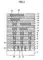
- FIG. 1 is a schematic cross-sectional view of one example of the semiconductor device of the invention.
- the substrate 1 is a Si semiconductor substrate such as Si substrate or SOI (Si-on-insulator) substrate, but it may be a compound semiconductor substrate such as SiGe or GaAs.
- Interlayer insulating films include the interlayer insulating film 2 of the contact layer, interlayer insulating films 3, 5, 7, 9, 11, 13, 15 and 17 of the interconnection layers, and the interlayer insulating films 4, 6, 8, 10, 12, 14 and 16 of the via layers.
- the interconnection layers corresponding to the lowermost interlayer insulating film 3 through the uppermost interlayer insulating film 17 are abbreviated as M1, M2, M3, M4, M5, M6, M7 and M8, respectively.
- the via layers corresponding to the lowermost interlayer insulating film 4 through the uppermost interlayer insulating film 16 are abbreviated as V1, V2, V3, V4, V5, V6 and V7, respectively.
- the via plug 19 comprises a metal. Copper interconnection usually comprises copper.
- the parts expressed with the same pattern without numbering as the via plug 19 indicate via plugs.
- the contact plug 20 is connected to the gate of a transistor (not illustrated) formed on the top surface of the substrate 1 or to the substrate.
- the interconnection layers and the via layers are alternately stacked, and multilayer interconnections generally indicate M1 and layers thereabove. In general, M1 to M3 are called local interconnections, M4 and M5 are called intermediate interconnections or semi-global interconnections, and M6 to M8 are called global interconnections.
- the porous film of the invention can be used as one or more of the inter-level insulating films 3, 5, 7, 9, 11, 13, 15 and 17 of the interconnection layers or the inter-level insulating films 4, 6, 8, 10, 12, 14, and 16 of the via layers.
- the porous film of the invention when used for the interlayer insulating film 3 of the interconnection layer (M1), the interconnection capacitance between the metal interconnection 21 and the metal interconnection 22 can be greatly reduced.
- the porous film of the present invention is used for the interlayer insulating film 4 of the via layer (V1), the interconnection capacitance between the metal interconnection 23 and the metal interconnection 24 can be greatly reduced.
- the use of the low-dielectric-constant porous film of the invention as an interconnection layer can greatly reduce the metal interconnection capacitance in the same layer.
- the use of the low-dielectric-constant porous film of the invention as a via layer can greatly reduce the interlayer capacitance between the upper and lower metal interconnections.
- the use of the porous film of the invention for all of the interconnection layers and via layers can greatly reduce the parasitic capacitance of the interconnections.
- the use of the porous film of the invention as insulating films of the interconnections therefore can prevent occurrence of a conventional problem, that is, an increase in the dielectric constant resulting from the moisture absorption of the porous film during the formation of multilayered interconnections by stacking porous films.
- the semiconductor device can perform high-speed and low-power operations.
- the porous film of the invention has high mechanical strength, the use of it can improve the mechanical strength of a semiconductor device, thereby greatly improving the production yield and the reliability of the semiconductor device.
- a mixture of 14.6 g of tetraethoxysilane and 25.4 g of a 1 mol/L aqueous solution of tetrapropylammonium hydroxide was stirred at room temperature for 3 days.
- the reaction mixture was stirred at 75°C for 12 hours to obtain a colorless zeolite sol.
- the particle size of the resulting sol was attempted to be measured by a submicron particle-size analyzer (measurement capability of 3 nm) but the whole particle size distribution could not be obtained because the bottom edge of the particle size distribution was 5 nm.
- a mixture of 70 g of ethanol, 35 g of ultrapure water and 3.9 g of 20 wt% tetramethylammonium hydroxide was stirred at 55°C.
- a mixture of 97 g of tetraethoxysilane, 73 g of methyltrimethoxysilane and 236 g of ethanol, and another mixture of 35 g of a 20 wt% aqueous tetramethylammonium hydroxide solution, 400 g of ethanol and 310 g of ultrapure water were added dropwise simultaneously over 2 hours.
- the particle size of the resulting polysiloxane particles dispersed in water-ethanol was attempted to be measured by a submicron particle-size analyzer (measurement capability: 3 nm) but the whole particle size distribution could not be measured because the bottom edge of the particle size distribution was 5 nm.
- the method for forming a porous-film-forming composition according to the invention is effective for the preparation of a material for forming a low-dielectric-constant insulating film having high mechanical strength.
- the porous-film-forming composition according to the invention is effective as a material for forming a low-dielectric-constant insulating film having high mechanical strength.
- the method for forming a porous film according to the invention is effective for preparing a material for forming a low-dielectric-constant insulating film having high mechanical strength.
- the porous film according to the invention is effective as a material for forming a low-dielectric-constant insulating film having high mechanical strength.
- the semiconductor device according to the invention is effective as a high performance semiconductor device capable of actualizing high-speed low-power-consumption operation.
Landscapes
- Chemical & Material Sciences (AREA)
- Chemical Kinetics & Catalysis (AREA)
- Organic Chemistry (AREA)
- Engineering & Computer Science (AREA)
- Materials Engineering (AREA)
- Wood Science & Technology (AREA)
- Life Sciences & Earth Sciences (AREA)
- Health & Medical Sciences (AREA)
- Medicinal Chemistry (AREA)
- Polymers & Plastics (AREA)
- Internal Circuitry In Semiconductor Integrated Circuit Devices (AREA)
- Formation Of Insulating Films (AREA)
- Porous Artificial Stone Or Porous Ceramic Products (AREA)
- Silicon Compounds (AREA)
Claims (3)
- Verfahren zur Herstellung einer einen porösen Film bildenden Zusammensetzung, umfassend:einen Schritt zum Herstellen der Komponente A;einen Schritt, um der Komponente A Vernetzbarkeit zu verleihen; undeinen Schritt zum temporären Abbrechen der Vernetzbarkeit, wobeidie Komponente A gewählt ist aus der Gruppe bestehend aus Polysiloxan-, Siliziumdioxid- und Zeolith-Partikeln, dadurch gekennzeichnet, dassder Schritt zum Verleihen von Vernetzbarkeit von Komponente A die Zugabe von Komponente B umfasst, die eine Organosiliziumverbindung ist und dadurch gekennzeichnet, dassder Schritt des temporären Abbrechens der Vernetzbarkeit die Zugabe einer Carbonsäure mit mindestens zwei Carboxylgruppen umfasst.
- Verfahren zur Herstellung einer einen porösen Film bildenden Zusammensetzung nach Anspruch 1, worin der Schritt des temporären Abbrechens der Vernetzbarkeit die Zugabe einer Carbonsäure umfasst, gewählt aus der Gruppe bestehend aus Oxalsäure, Malonsäure, Malonsäureanhydrid, Maleinsäure, Maleinsäureanhydrid, Fumarsäure, Glutarsäure, Glutarsäureanhydrid, Citraconsäure, Citraconsäureanhydrid, Itaconsäure, Itaconsäureanhydrid und Adipinsäure.
- Verfahren zur Herstellung eines porösen Films, umfassend die Schritte- Herstellung einer einen porösen Film bildenden Zusammensetzung wie in Anspruch 1 oder 2 beschrieben,- Aufbringen der einen porösen Film bildenden Zusammensetzung auf ein Substrat, um einen Film zu bilden;- Trocknen des Films; und- Vernetzen der Komponente A, zusammen mit dem Entfernen des vernetzbaren Inhibitors durch Erhitzen des getrockneten Films.
Applications Claiming Priority (2)
| Application Number | Priority Date | Filing Date | Title |
|---|---|---|---|
| JP2004017994 | 2004-01-27 | ||
| JP2004017994A JP4157048B2 (ja) | 2004-01-27 | 2004-01-27 | 多孔質膜形成用組成物、その製造方法、多孔質膜及び半導体装置 |
Publications (2)
| Publication Number | Publication Date |
|---|---|
| EP1559761A1 EP1559761A1 (de) | 2005-08-03 |
| EP1559761B1 true EP1559761B1 (de) | 2011-03-09 |
Family
ID=34650752
Family Applications (1)
| Application Number | Title | Priority Date | Filing Date |
|---|---|---|---|
| EP05250339A Expired - Lifetime EP1559761B1 (de) | 2004-01-27 | 2005-01-24 | Poröse filmbildende Zusammensetzung, Verfahren zur Herstellung dieser Zusammensetzung, poröser Film und Halbleiterbauelement |
Country Status (6)
| Country | Link |
|---|---|
| US (1) | US7402621B2 (de) |
| EP (1) | EP1559761B1 (de) |
| JP (1) | JP4157048B2 (de) |
| CN (1) | CN100467541C (de) |
| DE (1) | DE602005026738D1 (de) |
| TW (1) | TWI356809B (de) |
Families Citing this family (20)
| Publication number | Priority date | Publication date | Assignee | Title |
|---|---|---|---|---|
| DE102005040323A1 (de) * | 2005-08-25 | 2007-03-15 | Wacker Chemie Ag | Organopolysiloxane und ein Verfahren zu ihrer Herstellung |
| JP2008201832A (ja) * | 2007-02-16 | 2008-09-04 | Shin Etsu Chem Co Ltd | シロキサン重合体とその製造方法、該重合体を含有する多孔質膜形成用塗布液ならびに多孔質膜と、該多孔質膜を用いた半導体装置 |
| JP2008201833A (ja) * | 2007-02-16 | 2008-09-04 | Shin Etsu Chem Co Ltd | 膜形成用組成物、低誘電率絶縁膜、低誘電率絶縁膜の形成方法及び半導体装置 |
| JP2008205008A (ja) * | 2007-02-16 | 2008-09-04 | Shin Etsu Chem Co Ltd | 半導体層間絶縁膜形成用組成物とその製造方法、膜形成方法と半導体装置 |
| JP5231748B2 (ja) * | 2007-04-03 | 2013-07-10 | 信越化学工業株式会社 | ゼオライト微粒子の製造方法、安定化されたゼオライト及びその利用方法 |
| JP4866290B2 (ja) * | 2007-04-03 | 2012-02-01 | 信越化学工業株式会社 | ゼオライト含有膜の製造方法 |
| JP5096233B2 (ja) * | 2008-05-30 | 2012-12-12 | 信越化学工業株式会社 | 有機酸化ケイ素系微粒子及びその製造方法、多孔質膜形成用組成物、多孔質膜及びその形成方法、並びに半導体装置 |
| JP2009286935A (ja) * | 2008-05-30 | 2009-12-10 | Shin-Etsu Chemical Co Ltd | 有機酸化ケイ素微粒子及びその製造方法、多孔質膜形成用組成物、多孔質膜及びその形成方法、並びに半導体装置 |
| JP4947316B2 (ja) | 2008-08-15 | 2012-06-06 | 信越化学工業株式会社 | 基板の接合方法並びに3次元半導体装置 |
| US9260571B2 (en) * | 2012-05-24 | 2016-02-16 | Lawrence Livermore National Security, Llc | Hybrid polymer networks as ultra low ‘k’ dielectric layers |
| JP6599699B2 (ja) * | 2014-12-26 | 2019-10-30 | 日東電工株式会社 | 触媒作用を介して結合した空隙構造フィルムおよびその製造方法 |
| JP6612563B2 (ja) | 2014-12-26 | 2019-11-27 | 日東電工株式会社 | シリコーン多孔体およびその製造方法 |
| JP6604781B2 (ja) | 2014-12-26 | 2019-11-13 | 日東電工株式会社 | 積層フィルムロールおよびその製造方法 |
| JP6713871B2 (ja) | 2015-07-31 | 2020-06-24 | 日東電工株式会社 | 光学積層体、光学積層体の製造方法、光学部材、画像表示装置、光学部材の製造方法および画像表示装置の製造方法 |
| JP6713872B2 (ja) | 2015-07-31 | 2020-06-24 | 日東電工株式会社 | 積層フィルム、積層フィルムの製造方法、光学部材、画像表示装置、光学部材の製造方法および画像表示装置の製造方法 |
| JP6892744B2 (ja) | 2015-08-24 | 2021-06-23 | 日東電工株式会社 | 積層光学フィルム、積層光学フィルムの製造方法、光学部材、および画像表示装置 |
| JP7152130B2 (ja) | 2015-09-07 | 2022-10-12 | 日東電工株式会社 | 低屈折率層、積層フィルム、低屈折率層の製造方法、積層フィルムの製造方法、光学部材および画像表示装置 |
| WO2017122465A1 (ja) * | 2016-01-12 | 2017-07-20 | 東レ・ファインケミカル株式会社 | シリコーン重合体の製造方法 |
| EP3597710B1 (de) * | 2018-07-18 | 2021-08-18 | Inkron OY | Neuartige polysiloxanzusammensetzungen und verwendungen davon |
| CN117343638A (zh) * | 2022-06-27 | 2024-01-05 | 上海艾深斯科技有限公司 | 来自含硅聚合物的多孔的旋涂式介电涂层材料 |
Family Cites Families (10)
| Publication number | Priority date | Publication date | Assignee | Title |
|---|---|---|---|---|
| JPS62220531A (ja) * | 1986-03-24 | 1987-09-28 | Central Glass Co Ltd | 被覆用組成物 |
| TW492989B (en) | 1993-03-19 | 2002-07-01 | Dow Corning | Stabilization of hydrogen silsesquioxane resin solutions |
| JP3813268B2 (ja) * | 1996-03-25 | 2006-08-23 | 触媒化成工業株式会社 | 低誘電率シリカ系被膜形成用塗布液および低誘電率被膜付基材 |
| US6639015B1 (en) * | 1998-09-01 | 2003-10-28 | Catalysts & Chemicals Industries Co., Ltd. | Coating liquid for forming a silica-containing film with a low-dielectric constant |
| JP4195773B2 (ja) | 2000-04-10 | 2008-12-10 | Jsr株式会社 | 層間絶縁膜形成用組成物、層間絶縁膜の形成方法およびシリカ系層間絶縁膜 |
| JP4117436B2 (ja) | 2000-04-10 | 2008-07-16 | Jsr株式会社 | 膜形成用組成物、膜の形成方法およびシリカ系膜 |
| JP4117441B2 (ja) | 2000-04-10 | 2008-07-16 | Jsr株式会社 | 膜形成用組成物の製造方法、膜形成用組成物、膜の形成方法およびシリカ系膜 |
| JP4143792B2 (ja) | 2000-05-08 | 2008-09-03 | Jsr株式会社 | 膜形成用組成物および絶縁膜形成用材料 |
| JP4530113B2 (ja) | 2000-07-06 | 2010-08-25 | Jsr株式会社 | 膜形成用組成物の製造方法、膜形成用組成物、膜の形成方法およびシリカ系膜 |
| JP2004161877A (ja) | 2002-11-13 | 2004-06-10 | Shin Etsu Chem Co Ltd | 多孔質膜形成用組成物、多孔質膜とその製造方法、層間絶縁膜及び半導体装置 |
-
2004
- 2004-01-27 JP JP2004017994A patent/JP4157048B2/ja not_active Expired - Lifetime
-
2005
- 2005-01-14 TW TW094101189A patent/TWI356809B/zh not_active IP Right Cessation
- 2005-01-24 DE DE602005026738T patent/DE602005026738D1/de not_active Expired - Lifetime
- 2005-01-24 EP EP05250339A patent/EP1559761B1/de not_active Expired - Lifetime
- 2005-01-24 US US11/041,780 patent/US7402621B2/en not_active Expired - Lifetime
- 2005-01-27 CN CNB2005100058855A patent/CN100467541C/zh not_active Expired - Fee Related
Also Published As
| Publication number | Publication date |
|---|---|
| JP4157048B2 (ja) | 2008-09-24 |
| DE602005026738D1 (de) | 2011-04-21 |
| CN1651515A (zh) | 2005-08-10 |
| US7402621B2 (en) | 2008-07-22 |
| TWI356809B (en) | 2012-01-21 |
| TW200526521A (en) | 2005-08-16 |
| EP1559761A1 (de) | 2005-08-03 |
| CN100467541C (zh) | 2009-03-11 |
| US20050165197A1 (en) | 2005-07-28 |
| JP2005216895A (ja) | 2005-08-11 |
Similar Documents
| Publication | Publication Date | Title |
|---|---|---|
| EP1559761B1 (de) | Poröse filmbildende Zusammensetzung, Verfahren zur Herstellung dieser Zusammensetzung, poröser Film und Halbleiterbauelement | |
| JP4225765B2 (ja) | 低誘電率非晶質シリカ系被膜の形成方法および該方法より得られる低誘電率非晶質シリカ系被膜 | |
| US20080290472A1 (en) | Semiconductor interlayer-insulating film forming composition, preparation method thereof, film forming method, and semiconductor device | |
| US7405459B2 (en) | Semiconductor device comprising porous film | |
| US20080118737A1 (en) | Composition for forming porous film, porous film and method for forming the same, interlevel insulator film, and semiconductor device | |
| WO2004044074A1 (ja) | 多孔質膜形成用組成物、多孔質膜とその製造方法、層間絶縁膜及び半導体装置 | |
| WO2007072750A1 (ja) | 低誘電率非晶質シリカ系被膜形成用塗布液および該塗布液から得られる低誘電率非晶質シリカ系被膜 | |
| JP4139710B2 (ja) | 多孔質膜形成用組成物、多孔質膜の製造方法、多孔質膜、層間絶縁膜、及び半導体装置 | |
| US7332446B2 (en) | Composition for forming porous film, porous film and method for forming the same, interlevel insulator film and semiconductor device | |
| EP1566417B1 (de) | Zusammensetzung zur bildung eines porösenfilms, poröser film, herstellverfahren dafür, zwischenschichtisolierfilm und halbleitervorrichtung | |
| JPH11302595A (ja) | 低誘電率シリカ系被膜形成用塗布液および低誘電率被膜付基材 | |
| JP2004307693A (ja) | 多孔質膜形成用組成物、多孔質膜の製造方法、多孔質膜、層間絶縁膜、及び半導体装置 | |
| JP4257141B2 (ja) | 多孔質膜形成用組成物、多孔質膜の製造方法、多孔質膜、層間絶縁膜、及び半導体装置 | |
| KR20170050165A (ko) | 실리카 막의 제조방법, 실리카 막 및 전자소자 | |
| JP2004269694A (ja) | 多孔質膜形成用組成物、多孔質膜の製造方法、多孔質膜、層間絶縁膜、及び半導体装置 | |
| JPH1129744A (ja) | シリカ系被膜形成用塗布液、その製造法及びシリカ系被膜 | |
| JP2002009066A (ja) | シリカ系被膜及びそれを用いた半導体装置 |
Legal Events
| Date | Code | Title | Description |
|---|---|---|---|
| PUAI | Public reference made under article 153(3) epc to a published international application that has entered the european phase |
Free format text: ORIGINAL CODE: 0009012 |
|
| AK | Designated contracting states |
Kind code of ref document: A1 Designated state(s): AT BE BG CH CY CZ DE DK EE ES FI FR GB GR HU IE IS IT LI LT LU MC NL PL PT RO SE SI SK TR |
|
| AX | Request for extension of the european patent |
Extension state: AL BA HR LV MK YU |
|
| 17P | Request for examination filed |
Effective date: 20051116 |
|
| AKX | Designation fees paid |
Designated state(s): DE FR GB NL |
|
| RAP1 | Party data changed (applicant data changed or rights of an application transferred) |
Owner name: PANASONIC CORPORATION Owner name: SHIN-ETSU CHEMICAL CO., LTD. |
|
| GRAP | Despatch of communication of intention to grant a patent |
Free format text: ORIGINAL CODE: EPIDOSNIGR1 |
|
| RIN1 | Information on inventor provided before grant (corrected) |
Inventor name: HAMADA, YOSHITAKA Inventor name: OGIHARA, TSUTOMU Inventor name: YAGIHASHI, FUJIO Inventor name: SASAGO, MASARU Inventor name: IWABUCHI, MOTOAKI Inventor name: ASANO, TAKESHI Inventor name: NAKAGAWA, HIDEO |
|
| GRAS | Grant fee paid |
Free format text: ORIGINAL CODE: EPIDOSNIGR3 |
|
| GRAA | (expected) grant |
Free format text: ORIGINAL CODE: 0009210 |
|
| AK | Designated contracting states |
Kind code of ref document: B1 Designated state(s): DE FR GB NL |
|
| REG | Reference to a national code |
Ref country code: GB Ref legal event code: FG4D |
|
| REF | Corresponds to: |
Ref document number: 602005026738 Country of ref document: DE Date of ref document: 20110421 Kind code of ref document: P |
|
| REG | Reference to a national code |
Ref country code: DE Ref legal event code: R096 Ref document number: 602005026738 Country of ref document: DE Effective date: 20110421 |
|
| REG | Reference to a national code |
Ref country code: NL Ref legal event code: VDEP Effective date: 20110309 |
|
| PG25 | Lapsed in a contracting state [announced via postgrant information from national office to epo] |
Ref country code: NL Free format text: LAPSE BECAUSE OF FAILURE TO SUBMIT A TRANSLATION OF THE DESCRIPTION OR TO PAY THE FEE WITHIN THE PRESCRIBED TIME-LIMIT Effective date: 20110309 |
|
| PLBE | No opposition filed within time limit |
Free format text: ORIGINAL CODE: 0009261 |
|
| STAA | Information on the status of an ep patent application or granted ep patent |
Free format text: STATUS: NO OPPOSITION FILED WITHIN TIME LIMIT |
|
| 26N | No opposition filed |
Effective date: 20111212 |
|
| REG | Reference to a national code |
Ref country code: DE Ref legal event code: R097 Ref document number: 602005026738 Country of ref document: DE Effective date: 20111212 |
|
| REG | Reference to a national code |
Ref country code: FR Ref legal event code: PLFP Year of fee payment: 11 |
|
| REG | Reference to a national code |
Ref country code: FR Ref legal event code: PLFP Year of fee payment: 12 |
|
| PGFP | Annual fee paid to national office [announced via postgrant information from national office to epo] |
Ref country code: FR Payment date: 20151208 Year of fee payment: 12 |
|
| PGFP | Annual fee paid to national office [announced via postgrant information from national office to epo] |
Ref country code: DE Payment date: 20160119 Year of fee payment: 12 |
|
| PGFP | Annual fee paid to national office [announced via postgrant information from national office to epo] |
Ref country code: GB Payment date: 20160120 Year of fee payment: 12 |
|
| REG | Reference to a national code |
Ref country code: DE Ref legal event code: R119 Ref document number: 602005026738 Country of ref document: DE |
|
| GBPC | Gb: european patent ceased through non-payment of renewal fee |
Effective date: 20170124 |
|
| REG | Reference to a national code |
Ref country code: FR Ref legal event code: ST Effective date: 20170929 |
|
| PG25 | Lapsed in a contracting state [announced via postgrant information from national office to epo] |
Ref country code: FR Free format text: LAPSE BECAUSE OF NON-PAYMENT OF DUE FEES Effective date: 20170131 |
|
| PG25 | Lapsed in a contracting state [announced via postgrant information from national office to epo] |
Ref country code: GB Free format text: LAPSE BECAUSE OF NON-PAYMENT OF DUE FEES Effective date: 20170124 Ref country code: DE Free format text: LAPSE BECAUSE OF NON-PAYMENT OF DUE FEES Effective date: 20170801 |