EP1555854A2 - Dispersions-Elektrolumineszierendes Element - Google Patents
Dispersions-Elektrolumineszierendes Element Download PDFInfo
- Publication number
- EP1555854A2 EP1555854A2 EP05075366A EP05075366A EP1555854A2 EP 1555854 A2 EP1555854 A2 EP 1555854A2 EP 05075366 A EP05075366 A EP 05075366A EP 05075366 A EP05075366 A EP 05075366A EP 1555854 A2 EP1555854 A2 EP 1555854A2
- Authority
- EP
- European Patent Office
- Prior art keywords
- layer
- light
- luminescence
- transmitting
- dispersion
- Prior art date
- Legal status (The legal status is an assumption and is not a legal conclusion. Google has not performed a legal analysis and makes no representation as to the accuracy of the status listed.)
- Withdrawn
Links
Images


Classifications
-
- H—ELECTRICITY
- H05—ELECTRIC TECHNIQUES NOT OTHERWISE PROVIDED FOR
- H05B—ELECTRIC HEATING; ELECTRIC LIGHT SOURCES NOT OTHERWISE PROVIDED FOR; CIRCUIT ARRANGEMENTS FOR ELECTRIC LIGHT SOURCES, IN GENERAL
- H05B33/00—Electroluminescent light sources
- H05B33/12—Light sources with substantially two-dimensional [2D] radiating surfaces
- H05B33/26—Light sources with substantially two-dimensional [2D] radiating surfaces characterised by the composition or arrangement of the conductive material used as an electrode
-
- H—ELECTRICITY
- H05—ELECTRIC TECHNIQUES NOT OTHERWISE PROVIDED FOR
- H05B—ELECTRIC HEATING; ELECTRIC LIGHT SOURCES NOT OTHERWISE PROVIDED FOR; CIRCUIT ARRANGEMENTS FOR ELECTRIC LIGHT SOURCES, IN GENERAL
- H05B33/00—Electroluminescent light sources
- H05B33/12—Light sources with substantially two-dimensional [2D] radiating surfaces
- H05B33/14—Light sources with substantially two-dimensional [2D] radiating surfaces characterised by the chemical or physical composition or the arrangement of the electroluminescent material, or by the simultaneous addition of the electroluminescent material in or onto the light source
- H05B33/145—Arrangements of the electroluminescent material
-
- H—ELECTRICITY
- H05—ELECTRIC TECHNIQUES NOT OTHERWISE PROVIDED FOR
- H05B—ELECTRIC HEATING; ELECTRIC LIGHT SOURCES NOT OTHERWISE PROVIDED FOR; CIRCUIT ARRANGEMENTS FOR ELECTRIC LIGHT SOURCES, IN GENERAL
- H05B33/00—Electroluminescent light sources
- H05B33/12—Light sources with substantially two-dimensional [2D] radiating surfaces
- H05B33/22—Light sources with substantially two-dimensional [2D] radiating surfaces characterised by the chemical or physical composition or the arrangement of auxiliary dielectric or reflective layers
-
- H—ELECTRICITY
- H05—ELECTRIC TECHNIQUES NOT OTHERWISE PROVIDED FOR
- H05B—ELECTRIC HEATING; ELECTRIC LIGHT SOURCES NOT OTHERWISE PROVIDED FOR; CIRCUIT ARRANGEMENTS FOR ELECTRIC LIGHT SOURCES, IN GENERAL
- H05B33/00—Electroluminescent light sources
- H05B33/12—Light sources with substantially two-dimensional [2D] radiating surfaces
- H05B33/26—Light sources with substantially two-dimensional [2D] radiating surfaces characterised by the composition or arrangement of the conductive material used as an electrode
- H05B33/28—Light sources with substantially two-dimensional [2D] radiating surfaces characterised by the composition or arrangement of the conductive material used as an electrode of translucent electrodes
Definitions
- the present invention relates to a dispersion-type electroluminescence element (dispersion-type EL element) for use in various electronic appliances as back lighting for the display section or the operating section.
- FIG. 16 is a cross sectional view of a conventional dispersion-type EL element.
- a light-transmitting electrode layer 2 of indium tin oxide hereinafter referred to as ITO is formed through a sputtering process or an electron beam method.
- a luminescence layer 3 comprising a fluorocarbon rubber, cyano-group resin, or the like dielectric resin having a high permittivity dispersed with zinc sulfide or the like fluorescent powder as the luminous body, a dielectric layer 4 of dielectric resin having a high permittivity dispersed with barium titanate or the like dielectric powder, a back electrode layer 5 composed of silver, carbon-resin group or the like conductive material connected with the dielectric layer 4, and an insulation layer 6 composed of epoxy resin, polyester resin or the like material are formed one layer after the other in the order by a printing process.
- Wiring patterns 7A, 7B composed of silver or a conductive material of carbon-resin group are connected at the end portion to the light-transmitting electrode layer 2 and the back electrode layer 5, respectively.
- a dispersion-type EL element of the above-described structure When a dispersion-type EL element of the above-described structure is incorporated in an electronic appliance and an AC voltage is provided from a circuit (not shown) of the appliance on the wiring patterns 7A and 7B, which being connected respectively with the light-transmitting electrode layer 2 and the back electrode layer 5, the luminescence layer 3 of the dispersion-type EL element is driven to generate light.
- the light illuminates a display window, a liquid crystal display panel, etc. from behind.
- the display or an operating section can be easily recognized or identified even in a dark operational environment.
- Color of a light to be emitted from a dispersion-type EL element is determined by a kind of fluorescent powder dispersed in the luminescence layer 3 made of a dielectric resin having a high permittivity.
- the luminescence color can be converted into a color other than the intrinsic color of the fluorescent powder, by dispersing a fluorescent dye or a fluorescent pigment in the dielectric resin having a high permittivity, or by tinting the insulation film 1.
- a dispersion-type EL element having the above-described conventional structure only a single color is available although a luminescence color can be converted into other color by dispersing a fluorescent dye or a fluorescent pigment in the dielectric resin having a high permittivity forming the luminescence layer 3, or by tinting the insulation film 1.
- a plurality of luminescence colors are needed, a plurality of dispersion-type EL elements have to be installed in an electronic appliance. This incurs an increased number of parts in an appliance, which leads to an additional cost and time for the fabricating operation. Thus the total cost goes higher.
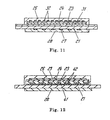
- FIG. 17 Another conventional dispersion-type EL element is shown in FIG. 17.
- a light-transmitting electrode layer 102 of ITO or the like material is provided in the form of thin film by a vacuum sputtering process or the like method.
- a luminescence layer 103 comprising a cyano-group resin or a fluorocarbon rubber group resin having a high permittivity dispersed with granular fluorescent powder such as a copper-doped zinc sulfide, etc.
- a dielectric layer 104 comprising a synthetic resin of the same group as the material of luminescence layer 103 dispersed with barium titanate or the like powder of high permittivity are formed respectively in the order by a coating process.
- a back electrode layer 105 composed of a paste of silver-resin group or a carbon-resin group material and an insulation layer 106 for protecting the back electrode layer 105 from contacting with outside element are formed respectively.
- an outlet electrode 107 of the light-transmitting electrode layer 102 and an outlet electrode 108 of the back electrode layer 105 are formed respectively.
- an AC voltage is applied between the outlet electrode 107 and the outlet electrode 108, the fluorescent powder being dispersed in the luminescence layer 103 is driven to produce a plane luminescence at the light-transmitting insulation layer 101 side.
- a conventional dispersion-type EL element (Japanese Patent Publication No.60-130097) comprises a light-transmitting electrode layer 109 disposed in the form of a number of stripes, as shown in FIG. 18(a).
- the electrode stripes in the odd number rows are connected together at one end, while those in the even number rows are connected together at the other end; thus, the light-transmitting electrode layer 109 is formed of two comb-shape electrodes 110 and 111 integrated into one entity without making mutual contact to each other.
- a luminescence layer 112 comprising two different luminescence colors is provided on the comb-shape electrodes 110, 111 in an arrangement where the luminescence color 112A is located on the odd number rows, while the luminescence color 112B is on the even number rows, as illustrated in FIG. 18(b).
- a multi-color luminescence is made available by applying independent voltages on two respective comb-shape electrodes 110, 111.
- the luminescence would appear to the eyes in a striped pattern rather than a plane luminescence when a voltage is applied on either one of the light-transmitting electrodes 110, 111 for producing a single-color luminescence.
- the luminescence can hardly be recognized as a plane luminescence.
- the thickness of the luminescence layer 112 is great and the surface condition is bumpy.
- the luminous bodies 112A, 112B of two different colors alternately in a stripe form through a printing process, if there is a small deviation in the dimensions edges of the adjacent layers of different colors would readily be overlapped and the layer thickness of the overlapped portion increases, which makes the surface condition even bumpier. Then the printing of dielectric layer and back electrode layer on the luminescence layer would become difficult.
- the electrode-to-electrode distance formed by the light-transmitting electrode layer and the back electrode layer becomes widely varied from place to place; which results in an uneven electrode-gap between the light-transmitting electrode layer and the back electrode layer, consequently an uneven luminescence would arise.
- the present invention addresses the above-described drawbacks, and aims to offer a dispersion-type EL element that is capable of providing multiple colors in a homogeneous plane luminescence without accompanying an outstanding striped-appearance. More advantages of the dispersion-type EL element in accordance with the present invention include that mounting of the EL element on an electronic appliance is easy and that the manufacturing cost is low.
- a dispersion-type EL element of the present invention is formed of a plurality of light-transmitting electrode layers and a plurality of luminescence layers composed of a dielectric resin having a high permittivity dispersed with fluorescent powder, each one of the respective layers being provided alternately one after the other over the whole region, or in a certain specific region, of one of the surfaces of a light-transmitting insulation film, and a back electrode layer is formed by a printing process on the last layer of the luminescence layers.
- two light-transmitting electrode layers having a comb shape of fine lines without making contact to each other, each of the electrode layers being capable of having different voltages independently to each other, are formed on one surface of a light-transmitting insulation film, and a luminescence layer of a single luminescence color is provided on the electrode layers; while, on the other surface of the light-transmitting insulation film, a color-conversion layer of a fine-teeth comb shape is provided in a location corresponding to at least one of the two light-transmitting electrode layers having a comb shape of fine lines, and a light diffusion layer is formed covering the outer surface.
- a dispersion-type EL element that is capable of providing several kinds of luminescence colors can be offered at a low cost.
- the plane luminescence provided by the EL element in a plurality of colors is homogeneous and stripes can hardly be recognized by the eyes in a normal operating environment.
- FIG. 1 is a cross sectional view of a dispersion-type EL element in accordance with a first exemplary embodiment of the present invention.
- FIG. 2 is a perspective view of the dispersion-type EL element.
- a plurality of light-transmitting electrode layers 12A, 12B formed of flexible light-transmitting resin, such as phenoxy resin, epoxy resin, fluorocarbon rubber, etc., dispersed with needle ITO or the like light-transmitting conductive powder, and a plurality of luminescence layers 13A, 13B each having different luminescence color composed of fluoro-carbon rubber, cyano-group resin or the like dielectric resin having a high permittivity dispersed with zinc sulfide or other fluorescent powder as the luminous body are formed alternately one after the other by a printing process on the whole surface, or in a certain specific region, of one of the surfaces of a flexible light-transmitting insulation film 1 composed of polyethylene telephtalate or the like.
- a back electrode layer 14 composed of silver or a carbon-resin group conductive material connected to the luminescence layer 13B, and an insulation layer 15 composed of epoxy resin, polyester resin or the like material are further formed one after the other by a printing process.
- the end portions of wiring patterns 16A, 16B, 16C composed of silver or a carbon-resin group conductive material are connected respectively with the light-transmitting electrode layers 12A, 12B and the back electrode layer 14 to complete a finished dispersion-type EL element.
- the respective luminescence layers 13A, 13B produce different luminescence colors because each of the fluorescent powders dispersed in respective dielectric resin layers of high permittivity has its own luminescence color different to each other, or the color is converted to a different color by a fluorescent dye or a fluorescent pigment added in the dielectric resin of high permittivity.
- the luminescence color of luminescence layer 13A is blue and that of luminescence layer 13B is orange
- the luminescence layer 13A when an AC voltage is applied between the wiring patterns 16A and 16B, which are connected with the light-transmitting electrode layers 12A and 12B, the luminescence layer 13A produces blue light
- the luminescence layer 13B when an AC voltage is applied between the wiring patterns 16B and 16C, which are connected with the light-transmitting electrode layer 12B and the back electrode layer 14, the luminescence layer 13B produces orange light
- an AC voltage is applied on all of the wiring patterns 16A, 16B and 16C both of the luminescence layers 13A and 13B produce lights of their own colors, which lights are composed to make yellow color.
- a dispersion-type EL element of the present embodiment where a plurality of light-transmitting electrode layers 12A, 12B and a plurality of luminescence layers 13A, 13B of different colors are stacked alternately one after the other by a printing process, luminescence of various different colors can be produced. This enables to offer a multi-color dispersion-type EL element at an inexpensive cost.
- the light-transmitting electrode layers 12A, 12B are formed using a flexible light-transmitting resin by a printing process, alike the other layers which are formed of flexible resin dispersed with various element powders, the dispersion-type EL element is flexible enough to be mounted on a curved surface, or may even be bent.
- Tinting of the light-transmitting electrode layers 12A, 12B with fluorescent dye or fluorescent pigment added therein enables to create more varieties of colors, in combination with the luminescence colors from luminescence layers 13A, 13B.
- a dielectric layer 17A, 17B composed of the same material as the luminescence layer 13A, 13B, which being a fluorocarbon rubber, a cyano-group resin or the like dielectric resin of high permittivity, dispersed with barium titanate or the like dielectric powder, over the luminescence layer 13A, 13B by a printing process, as shown in FIG. 3, makes the insulation between electrode layers surer, and, at the same time, a voltage effecting on the luminescence layer 13A, 13B becomes higher than on the dielectric layer 17A, 17B, which brings about an increased luminous intensity of the luminescence layer.
- the quantity of barium titanate contained in the first dielectric layer 17A is too high the light from the second luminescence layer 13B is blocked. Therefore, it is preferred that the quantity of barium titanate contained in the second dielectric layer 17B is 60 - 95 weight % of the dielectric resin of high permittivity, while the quantity of barium titanate contained in the first dielectric layer 17A is 2 - 60 weight %.
- the blocking of the light coming from luminescence layer can be suppressed to a minimum by using a fine-grain barium titanate, titanium oxide or the like dielectric powder of high permittivity, the grain size should preferably be less than 0.1 ⁇ m, or a hydrolysis organic metal, such as barium ethoxide, titanium ethoxide, etc., which produces a dielectric metal oxide of high permittivity as a result of hydrolysis, for the dielectric powder to be dispersed in the dielectric resin of high permittivity in the dielectric layer 17A, 17B.
- a fine-grain barium titanate, titanium oxide or the like dielectric powder of high permittivity the grain size should preferably be less than 0.1 ⁇ m, or a hydrolysis organic metal, such as barium ethoxide, titanium ethoxide, etc., which produces a dielectric metal oxide of high permittivity as a result of hydrolysis, for the dielectric powder to be dispersed in the dielectric resin of high permittivity in the dielectric
- the luminous intensity can be enhanced by making the second dielectric layer 17B white; because the lights from the luminescence layers 13A and 13B are reflected by the white dielectric layer towards the insulation film.
- FIG. 4 is a cross sectional view of a dispersion-type EL element in accordance with a second exemplary embodiment of the present invention.
- the dispersion-type EL element comprises, alike the embodiment 1, a plurality of light-transmitting electrode layers 12A, 12B and a plurality of luminescence layers 13A, 13B provided alternately one after the other by a printing process on the whole surface, or in a certain specific region, of one of the surfaces of a light-transmitting insulation film 1, and a back electrode layer 14 and an insulation layer 15 are formed thereon; and the end portions of wiring pattern 16A, 16B, 16C (not shown) are connected respectively with the light-transmitting electrode layers 12A, 12B and the back electrode layer 14.
- the point of difference as compared with the embodiment 1 is that there is a light conversion layer 18 composed of polyester resin, epoxy resin, acrylic resin, phenoxy resin, fluoro-carbon rubber or the like material dispersed with fluorescent dye or fluorescent pigment, formed in between the second light-transmitting electrode layer 12B and the luminescence layer 13B by a printing process.
- the luminescence color of luminescence layers 13A, 13B is, for example, blue and the color conversion layer 18 is orange; when an AC voltage is applied between the wiring patterns 16A and 16B, which are connected with the light-transmitting electrode layers 12A, 12B, the luminescence layer 13A produces blue light.
- the luminescence layer 13B produces also blue light, but the light is converted into orange color by the light conversion layer 18.
- the blue color from luminescence layer 13A and the orange color from light conversion layer 18 are composed to produce yellow color.
- a dispersion-type EL element of the present embodiment where there is a color conversion layer 18 provided in between the second layer of the light-transmitting electrode layer 12B, or a layer after the second, and the luminescence layer 13B, the luminescence color from respective luminescence layers can be converted into other color. Therefore, varieties of colors may be produced out of the luminescence layers 13A, 13B having a same luminescence color. This enables to offer a multi-color dispersion-type EL element at an inexpensive cost.
- the luminescence layer 13B is sandwiched by the light-transmitting electrode layer 12B and the back electrode layer 14 with the color conversion layer 18 interposed, luminous intensity of the luminescence layer 13B decreases by approximately 5 - 30%.
- the deterioration of luminous intensity can be alleviated by a light-transmitting conductive layer 19 provided by a printing process over the color conversion layer 18, as illustrated in FIG. 5, which conductive layer being connected with the light-transmitting electrode layer 12B.
- the luminescence layer 13B is provided with an AC voltage direct from the light-transmitting conductive layer 19 and the back electrode layer 14.
- the layers may of course be provided in a structure of three, four or more number of stacked layers for producing more number of luminescence colors.
- the first light-transmitting electrode layer 12A may be formed by a sputtering process or an electron beam method.
- the second light-transmitting electrode layer which is formed on the luminescence layer 13A, it is difficult in practice to provide it thorough the sputtering or the electron beam method. Therefore, it is usually formed by a printing process.
- the sheet resistance value should preferably be lower than 1k ⁇ . However, no substantial deterioration is observed in the luminous intensity in so far as it is lower than approximately 50k ⁇ .
- composition and conversion of the luminescence colors may be carried out in more varieties of combinations. In this way, a dispersion-type EL element capable of producing more number of colors is provided.
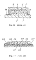
- FIG. 6 is a cross sectional view of a dispersion-type EL element in accordance with a third exemplary embodiment of the present invention.
- a light-transmitting electrode layer 22 is provided on one of the surfaces of an insulation film 21 in the form of stripes of fine lines by a printing process.
- a luminescence layer 23 of a single luminescence color, a dielectric layer 24, a back electrode layer 25 are printed one after the other.
- an insulation layer 26 is formed by a printing process covering the back electrode layer 25.
- a color conversion layer 27 is provided by a printing process in the form of stripes placed only in a location corresponding to the stripes of even number lines of the light-transmitting electrode layer 22.
- a light diffusion layer 28 is formed covering the color conversion layer 27, as illustrated in FIG. 6.
- FIG. 7 is a plan view of the light-transmitting electrode layer 22; among the fine lines of the comb-teeth light-transmitting electrode layer 22, coupled but without making contact to each other, formed on the insulation film 21, the electrode teeth 22A of odd number lines are connected together at one end to be coupled with an outlet electrode 29 provided at the same side as the end, while the electrode teeth 22B of even number lines are connected together at the other end to be coupled with an outlet electrode 29A provided at the same side as the other end.
- FIG. 8 shows a cross sectional view of the dispersion-type EL element, along the line Y - Y of FIG. 6.
- the outlet electrode 29 (29A) is connected with the light-transmitting electrode layer 22A (22B) at the end portion, and is disposed at an edge area of the insulation film 21 to be ready for connection with an outside circuit (not shown).
- another outlet electrode 30 coupled with the back electrode layer 25 is provided on the insulation film 21 at a place in one edge area so as not making contact with the outlet electrode 29, or 29A, of the light-transmitting electrode layer 22.
- FIG. 10 shows a pattern of the color conversion layer 27; stripe lines of the color conversion layer 27 are disposed only at the locations corresponding to the even number lines of electrodes 22B of the light-transmitting electrode layer 22 illustrated in FIG. 6.
- the light-transmitting electrode layer 22 is formed with a light-transmitting conductive paste of needle powder ITO having preferably a diameter of approximately 2 - 3 ⁇ m, dispersed in polyester resin, epoxy resin, acrylic resin, phenoxy resin, fluoro-carbon rubber resin, or the like material, the sheet resistance value of which layer should preferably be lower than 5k ⁇ /cm 2 , printed by a screen printing or the like process into a pattern of comb-teeth of fine lines coupled one tooth after the other without making contact to each other, and then dried.
- a light-transmitting conductive paste of needle powder ITO having preferably a diameter of approximately 2 - 3 ⁇ m, dispersed in polyester resin, epoxy resin, acrylic resin, phenoxy resin, fluoro-carbon rubber resin, or the like material, the sheet resistance value of which layer should preferably be lower than 5k ⁇ /cm 2 , printed by a screen printing or the like process into a pattern of comb-teeth of fine lines coupled one tooth after the other without
- the luminescence layer 23 is formed by screen-printing and drying a paste of EL fluorescent powder dispersed in cyanoethyl cellulose resin, cyanoethyl pullulan resin, fluoro-carbon rubber resin containing vinylidene fluoride, or the like material having a high permittivity.
- the dielectric layer 24 is formed by screen-printing and drying a paste of barium titanate or the like white fine-grain powder of high permittivity dispersed in a resin of the same group as used for the paste of luminescence layer 23.
- the back electrode layer 25 and the outlet electrodes 29, 29A, 30 are formed by screen-printing and drying a silver paste or a carbon paste for use in membrane switch, etc.
- the insulation layer 26 is formed by screen-printing and drying an electrically insulating paste of polyester, vinyl chloride, fluoro-carbon rubber, polyurethane, epoxy or the like material.
- the color conversion layer 27 is formed by screen-printing and drying a paste of fluorescent dye or fluorescent pigment having a preferred average grain diameter smaller than 10 ⁇ m dispersed in an insulating transparent resin such as polyester resin, epoxy resin, phenoxy resin, urethane resin, acrylic resin, polycarbonate resin, etc.
- the fluorescent pigment used In dispersing a fluorescent pigment in the color conversion layer 27, if the fluorescent pigment used has a grain diameter smaller than 30 ⁇ m, which being the average diameter of the EL fluorescent powder used in luminescence layer 23, it will produce a luminescence that has a line width finer than that of the striped pattern as referred to in BACKGROUND OF THE INVENTION. It is preferred, however, to use a fluorescent pigment whose grain diameter is smaller than 10 ⁇ m in average, if a pattern of higher stripe density is to be formed in order to produce a plane luminescence of even higher level of homogeneous representation.
- the light diffusion layer 28 may be provided, for example, by means of:
- the blue light produced in the luminescence layer 23 proceeds direct to the light diffusion layer 28, not going through the color conversion layer 27, to be diffused there and emitted to outside as blue light.
- the light-transmitting electrode layer 22 composed of two electrodes 22A, 22B having a comb shape of fine lines and the color conversion layer 27 can be provided in the form of fine lines of very small line width by the use of fine-grain powders of needle ITO, fluorescent dye or fluorescent pigment. Furthermore, as the lights are diffused at the light diffusion layer 28 the stripes are not outstanding to the eyes under normal operating conditions. Thus the three colors can be produced in a homogeneous plane luminescence.
- the paste for forming the luminescence layer may also be provided by using a synthetic resin tinted with a fluorescent dye or a fluorescent pigment.
- the formation of light-transmitting electrode layer has been described based on a printing process using a conductive paste, it may be provided instead by first forming a transparent thin-film of ITO, or tin oxide, through a sputtering or an electron beam method and then etching the thin-film into the comb shape of fine lines.
- FIG. 11 shows a cross sectional view of a dispersion-type EL element in accordance with a fourth exemplary embodiment of the present invention.
- the point of difference as compared with the embodiment 3 is in the shapes of light-transmitting electrode layer 31 and the back electrode layer 32.
- the light-transmitting electrode layer 31 is provided using the same material as that in the embodiment 3, but it is formed on one of the surfaces of an insulation film 21 covering the whole area.
- the back electrode layer 32 is provided using also the same material as that in the embodiment 3, viz. a paste containing silver powder or carbon powder of extremely fine grain size, but it is provided in a form similar to that of the light-transmitting electrode layer 22 in the embodiment 3, viz. it is provided on the dielectric layer 24 in two groups of comb shape of fine lines coupled one tooth after the other without making contact to each other; electrode lines of odd number rows are connected together at one end, while those of even number rows are connected together at the other end, to be coupled respectively with outlet electrodes (not shown) disposed in the same side of the respective ends.
- the luminescence color of luminescence layer 23 is blue
- color of the color conversion layer 27 is orange
- an AC voltage is applied between the light-transmitting electrode layer 31 and one of the two electrodes of the back electrode layers 32 having a comb shape of fine lines
- an AC voltage is applied between the light-transmitting electrode layer 31 and the other electrode of the back electrode layer 32
- an AC voltage is applied on the light-transmitting electrode layer 31 and both of the two electrodes of the back electrode layer 32 having a comb shape of fine lines, it produces a composite color, yellow-white.
- the back electrode layer 32 composed of two groups of comb shape of fine lines and the light conversion layer 27 can be provided in the form of fine lines of very small line width by the use of fine-grain powders of silver, carbon, fluorescent dye or fluorescent pigment. Furthermore, as the lights are diffused at the light diffusion layer 28 the stripes are not outstanding to the eyes under normal operating conditions. Thus the three colors can be produced in a homogeneous plane luminescence.
- FIG. 12 shows a cross sectional view of a dispersion-type EL element in accordance with a fifth exemplary embodiment of the present invention.
- the point of difference as compared with the element of embodiment 3 is in the position of color conversion layer 41.
- the light-transmitting electrode layer 22 is formed by printing on one of the surfaces of insulation film 21 and the color conversion layer 27 is formed by printing on the other surface
- a light-transmitting electrode layer 42 composed of two sets of fine lines of comb-teeth coupled one after the other is formed first on one surface of an insulation film 21 and then a color conversion layer 41 is formed by printing to cover the surface of one set of the electrode teeth lines.
- Other constituent portions of the present embodiment 5 remain the same as those of the embodiment 3.
- a dispersion-type EL element of the present embodiment 5 operates on the same operating principle as that of the embodiment 3; so detailed description of which is omitted here.
- the light-transmitting electrode layer 42 and the color conversion layer 41 of the present embodiment 5 are formed at a very fine line-width; therefore, a multiple number of colors are produced in a homogeneous plane luminescence, where the stripes are not seen outstanding from the eyes under a normal working environment.
- the color conversion layer 41 formed in stripes is printed direct on the light-transmitting electrode layer 42 of fine line comb-teeth shape, so the aligning can be made precisely with ease and occurrence of a possible dislocation between the color conversion layer 41 and the light-transmitting electrode layer 42 is prevented.
- the key constituent portion relevant to producing a multiple number of colors are formed at a high precision level, and displacement of colors is effectively eliminated.
- FIG. 13 shows a cross sectional view of an insulation film, a light-transmitting electrode layer having a comb shape of fine lines and a Thomson mould, which being key portions of a dispersion-type EL element in accordance with a sixth embodiment of the present invention.
- the point of difference as compared with the embodiment 3 is in the method of forming a light-transmitting electrode layer having a comb shape of fine lines.
- the light-transmitting electrode layer 51 having a comb shape of fine lines is provided by first forming a transparent conductive film of ITO or zinc oxide on the insulation film 52 over the whole area through sputtering or the like process, and then cutting the transparent conductive film using a Thomson mould 54 equipped with a blade 53.
- Other constituent portions of the present embodiment 6 remain the same as those of the embodiment 3.
- a dispersion-type EL element of the present embodiment operates on the same operating principle as that of the embodiment 3; so detailed description of which is omitted here.
- the light-transmitting electrode layer 51 composed of two groups of comb-teeth fine lines in the present embodiment 6 is provided by first forming a transparent conductive film on the insulation film 52 over the whole area through a sputtering process, and then cutting the transparent conductive film using a Thomson mould 54. In this way, the light-transmitting electrode layer 51 having comb-teeth fine lines of fine pitch can easily be provided without relying on an etching method, the facilities for which method is expensive. Thus, a multiple number of colors are produced in a homogeneous plane luminescence, where the stripes are not seen outstanding from the eyes under a normal working environment.
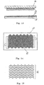
- FIG. 14 and FIG. 15 are plane views of a light-transmitting electrode layer having a comb-shape of fine lines and a color conversion layer, which being key portions of a dispersion-type EL element in accordance with a seventh exemplary embodiment of the present invention.
- the point of difference as compared with the embodiment 3 is in the shapes of light-transmitting electrode layer 61 and the color conversion layer 62.
- the light-transmitting electrode layer 61 composed of two groups of comb shape of fine lines coupled one tooth after the other without making contact to each other is provided on one of the surfaces of an insulation film 21, the comb-teeth lines taking a parallel wave form arrangement.
- the color conversion layer 62 of an identical parallel wave form is provided in a location corresponding to one of the two groups of electrode lines of light-transmitting electrode layer.
- Other constituent portions of the present embodiment 7 remain the same as those of the embodiment 3.
- a dispersion-type EL element of the present embodiment operates on the same operating principle as that of the embodiment 3; so detailed description of which is omitted here.
- a dispersion-type EL element of the present embodiment provides homogeneous plane luminescence in multiple colors without accompanying the striped luminescence recognizable by the eyes under normal operating conditions.
- the waving forms of the fine teeth-lines of the light-transmitting electrode layer 61 and the color conversion layer 62 improves the effect of diffusing a light by a light diffusion layer, thickness of the light diffusion layer needed to make the diffused light sufficiently homogeneous can be reduced.
- a light-transmitting electrode layer, a back electrode layer and a color conversion layer in a dispersion-type EL element of the present invention are provided by using fine-grain conductive material or fluorescent material having a grain size much smaller than that of fluorescent powder dispersed in the luminescence layer. Therefore, the light-transmitting electrode layer, the back electrode layer and the color conversion layer can be provided in a stripe form of fine lines having an extremely fine line-width that is much smaller than that of the stripes of a luminescence layer.
- a dispersion-type EL element capable of producing multiple number of colors in a homogeneous plane luminescence without accompanying the stripes recognizable by the eyes under a normal operating environment can be offered at low cost.
Landscapes
- Electroluminescent Light Sources (AREA)
Applications Claiming Priority (5)
| Application Number | Priority Date | Filing Date | Title |
|---|---|---|---|
| JP19851098A JP3885371B2 (ja) | 1998-07-14 | 1998-07-14 | 分散型el素子 |
| JP19851098 | 1998-07-14 | ||
| JP10249362A JP2000082587A (ja) | 1998-09-03 | 1998-09-03 | 分散型多色発光elランプ |
| JP24936298 | 1998-09-03 | ||
| EP99305368A EP0973358B1 (de) | 1998-07-14 | 1999-07-06 | Dispersions-Elektrolumineszierendes Element |
Related Parent Applications (2)
| Application Number | Title | Priority Date | Filing Date |
|---|---|---|---|
| EP99305368.5 Division | 1999-07-06 | ||
| EP99305368A Division EP0973358B1 (de) | 1998-07-14 | 1999-07-06 | Dispersions-Elektrolumineszierendes Element |
Publications (2)
| Publication Number | Publication Date |
|---|---|
| EP1555854A2 true EP1555854A2 (de) | 2005-07-20 |
| EP1555854A3 EP1555854A3 (de) | 2010-11-17 |
Family
ID=26511014
Family Applications (2)
| Application Number | Title | Priority Date | Filing Date |
|---|---|---|---|
| EP05075366A Withdrawn EP1555854A3 (de) | 1998-07-14 | 1999-07-06 | Dispersions-Elektrolumineszierendes Element |
| EP99305368A Expired - Lifetime EP0973358B1 (de) | 1998-07-14 | 1999-07-06 | Dispersions-Elektrolumineszierendes Element |
Family Applications After (1)
| Application Number | Title | Priority Date | Filing Date |
|---|---|---|---|
| EP99305368A Expired - Lifetime EP0973358B1 (de) | 1998-07-14 | 1999-07-06 | Dispersions-Elektrolumineszierendes Element |
Country Status (5)
| Country | Link |
|---|---|
| US (1) | US6479930B1 (de) |
| EP (2) | EP1555854A3 (de) |
| KR (2) | KR100316488B1 (de) |
| DE (1) | DE69935376T2 (de) |
| TW (1) | TW420965B (de) |
Cited By (1)
| Publication number | Priority date | Publication date | Assignee | Title |
|---|---|---|---|---|
| US8330348B2 (en) | 2005-10-31 | 2012-12-11 | Osram Opto Semiconductors Gmbh | Structured luminescence conversion layer |
Families Citing this family (47)
| Publication number | Priority date | Publication date | Assignee | Title |
|---|---|---|---|---|
| JP3887984B2 (ja) | 1999-02-05 | 2007-02-28 | 松下電器産業株式会社 | 多色発光分散型elランプ |
| US7301276B2 (en) * | 2000-03-27 | 2007-11-27 | Semiconductor Energy Laboratory Co., Ltd. | Light emitting apparatus and method of manufacturing the same |
| JP2002151270A (ja) * | 2000-11-07 | 2002-05-24 | Matsushita Electric Ind Co Ltd | Elランプ |
| JP4789341B2 (ja) * | 2001-03-30 | 2011-10-12 | 三洋電機株式会社 | 半導体装置及び半導体装置製造用マスク |
| CZ20021789A3 (cs) * | 2001-05-25 | 2003-01-15 | Michel Tramontana | Elektroluminiscenční systém a zařízení k jeho výrobě |
| KR100463702B1 (ko) * | 2001-09-27 | 2004-12-29 | 윈텍 주식회사 | 전기 발광소자 |
| JP2003317969A (ja) * | 2002-04-19 | 2003-11-07 | Print Labo Kk | El発光装置 |
| WO2003098975A1 (en) * | 2002-05-17 | 2003-11-27 | Print Labo Co., Ltd. | El light emitting device |
| GB2392558B (en) * | 2002-08-30 | 2004-11-10 | Tomy Co Ltd | Electroluminescence light emitting display system and electroluminescence light emitting sheet |
| JP2004119016A (ja) * | 2002-09-20 | 2004-04-15 | Semiconductor Energy Lab Co Ltd | 発光装置 |
| JP2004119015A (ja) * | 2002-09-20 | 2004-04-15 | Semiconductor Energy Lab Co Ltd | 発光装置およびその作製方法 |
| US20040099926A1 (en) * | 2002-11-22 | 2004-05-27 | Semiconductor Energy Laboratory Co., Ltd. | Semiconductor device, display device, and light-emitting device, and methods of manufacturing the same |
| DE10338502A1 (de) | 2003-08-21 | 2005-03-31 | Schreiner Group Gmbh & Co. Kg | Mehrfarb-Elektrolumineszenz-Element und Verfahren zu dessen Herstellung |
| DE10353679A1 (de) * | 2003-11-17 | 2005-06-02 | Siemens Ag | Kostengünstige, miniaturisierte Aufbau- und Verbindungstechnik für LEDs und andere optoelektronische Module |
| US7815854B2 (en) | 2004-04-30 | 2010-10-19 | Kimberly-Clark Worldwide, Inc. | Electroluminescent illumination source for optical detection systems |
| US7796266B2 (en) | 2004-04-30 | 2010-09-14 | Kimberly-Clark Worldwide, Inc. | Optical detection system using electromagnetic radiation to detect presence or quantity of analyte |
| US7625501B2 (en) * | 2004-05-18 | 2009-12-01 | Ifire Ip Corporation | Color-converting photoluminescent film |
| US20060138948A1 (en) * | 2004-12-27 | 2006-06-29 | Quantum Paper, Inc. | Addressable and printable emissive display |
| EP1836879A2 (de) * | 2004-12-27 | 2007-09-26 | Quantum Paper, Inc. | Adressierbares und druckbares emissives display |
| US20060138944A1 (en) * | 2004-12-27 | 2006-06-29 | Quantum Paper | Addressable and printable emissive display |
| US7586245B2 (en) | 2005-08-29 | 2009-09-08 | Osram Opto Semiconductors Gmbh | Using prismatic microstructured films for image blending in OLEDS |
| US7420323B2 (en) | 2005-10-31 | 2008-09-02 | Osram Opto Semiconductors Gmbh | Electroluminescent apparatus having a structured luminescence conversion layer |
| US7321193B2 (en) | 2005-10-31 | 2008-01-22 | Osram Opto Semiconductors Gmbh | Device structure for OLED light device having multi element light extraction and luminescence conversion layer |
| US20070097252A1 (en) * | 2005-10-31 | 2007-05-03 | Silverstein D A | Imaging methods, cameras, projectors, and articles of manufacture |
| US8415879B2 (en) | 2007-05-31 | 2013-04-09 | Nthdegree Technologies Worldwide Inc | Diode for a printable composition |
| US8877101B2 (en) | 2007-05-31 | 2014-11-04 | Nthdegree Technologies Worldwide Inc | Method of manufacturing a light emitting, power generating or other electronic apparatus |
| US8674593B2 (en) | 2007-05-31 | 2014-03-18 | Nthdegree Technologies Worldwide Inc | Diode for a printable composition |
| US9018833B2 (en) | 2007-05-31 | 2015-04-28 | Nthdegree Technologies Worldwide Inc | Apparatus with light emitting or absorbing diodes |
| US8809126B2 (en) | 2007-05-31 | 2014-08-19 | Nthdegree Technologies Worldwide Inc | Printable composition of a liquid or gel suspension of diodes |
| US9425357B2 (en) | 2007-05-31 | 2016-08-23 | Nthdegree Technologies Worldwide Inc. | Diode for a printable composition |
| US8852467B2 (en) | 2007-05-31 | 2014-10-07 | Nthdegree Technologies Worldwide Inc | Method of manufacturing a printable composition of a liquid or gel suspension of diodes |
| US8889216B2 (en) * | 2007-05-31 | 2014-11-18 | Nthdegree Technologies Worldwide Inc | Method of manufacturing addressable and static electronic displays |
| US8456393B2 (en) | 2007-05-31 | 2013-06-04 | Nthdegree Technologies Worldwide Inc | Method of manufacturing a light emitting, photovoltaic or other electronic apparatus and system |
| US9343593B2 (en) | 2007-05-31 | 2016-05-17 | Nthdegree Technologies Worldwide Inc | Printable composition of a liquid or gel suspension of diodes |
| US9534772B2 (en) | 2007-05-31 | 2017-01-03 | Nthdegree Technologies Worldwide Inc | Apparatus with light emitting diodes |
| US9419179B2 (en) | 2007-05-31 | 2016-08-16 | Nthdegree Technologies Worldwide Inc | Diode for a printable composition |
| US8846457B2 (en) | 2007-05-31 | 2014-09-30 | Nthdegree Technologies Worldwide Inc | Printable composition of a liquid or gel suspension of diodes |
| WO2009079004A1 (en) | 2007-12-18 | 2009-06-25 | Lumimove, Inc., Dba Crosslink | Flexible electroluminescent devices and systems |
| US8127477B2 (en) | 2008-05-13 | 2012-03-06 | Nthdegree Technologies Worldwide Inc | Illuminating display systems |
| US7992332B2 (en) * | 2008-05-13 | 2011-08-09 | Nthdegree Technologies Worldwide Inc. | Apparatuses for providing power for illumination of a display object |
| JP5440064B2 (ja) * | 2008-10-21 | 2014-03-12 | 東芝ライテック株式会社 | 照明装置 |
| JP5327601B2 (ja) | 2008-12-12 | 2013-10-30 | 東芝ライテック株式会社 | 発光モジュールおよび照明装置 |
| US8408724B2 (en) * | 2008-12-26 | 2013-04-02 | Toshiba Lighting & Technology Corporation | Light source module and lighting apparatus |
| US8820950B2 (en) * | 2010-03-12 | 2014-09-02 | Toshiba Lighting & Technology Corporation | Light emitting device and illumination apparatus |
| US10312731B2 (en) | 2014-04-24 | 2019-06-04 | Westrock Shared Services, Llc | Powered shelf system for inductively powering electrical components of consumer product packages |
| CN112996167A (zh) * | 2019-12-18 | 2021-06-18 | 京懋国际光电股份有限公司 | 电激发光装置 |
| CN118136615B (zh) * | 2024-05-06 | 2024-07-16 | 北京智芯微电子科技有限公司 | 薄膜电阻及其制备方法、电子器件、芯片和电子设备 |
Family Cites Families (14)
| Publication number | Priority date | Publication date | Assignee | Title |
|---|---|---|---|---|
| US3786307A (en) * | 1972-06-23 | 1974-01-15 | Atronics Corp | Solid state electroluminescent x-y display panels |
| JPS60130097A (ja) | 1983-12-16 | 1985-07-11 | 株式会社日立製作所 | El素子 |
| US4684353A (en) * | 1985-08-19 | 1987-08-04 | Dunmore Corporation | Flexible electroluminescent film laminate |
| US5184969A (en) * | 1988-05-31 | 1993-02-09 | Electroluminscent Technologies Corporation | Electroluminescent lamp and method for producing the same |
| JPH05135875A (ja) * | 1991-01-24 | 1993-06-01 | Kenwood Corp | 多色発光薄膜el素子 |
| US5652067A (en) * | 1992-09-10 | 1997-07-29 | Toppan Printing Co., Ltd. | Organic electroluminescent device |
| JPH06231882A (ja) * | 1993-02-01 | 1994-08-19 | Sharp Corp | 薄膜el素子 |
| JPH07176383A (ja) * | 1993-12-21 | 1995-07-14 | Casio Comput Co Ltd | エレクトロルミネッセンス素子 |
| JPH08153582A (ja) * | 1994-11-25 | 1996-06-11 | Nippon Seiki Co Ltd | 分散型電界発光素子 |
| WO1996025020A1 (en) * | 1995-02-06 | 1996-08-15 | Idemitsu Kosan Co., Ltd. | Multi-color light emission apparatus and method for production thereof |
| US6117529A (en) * | 1996-12-18 | 2000-09-12 | Gunther Leising | Organic electroluminescence devices and displays |
| US5874803A (en) * | 1997-09-09 | 1999-02-23 | The Trustees Of Princeton University | Light emitting device with stack of OLEDS and phosphor downconverter |
| JPH10189244A (ja) * | 1996-12-24 | 1998-07-21 | Casio Comput Co Ltd | エレクトロルミネセンス・パネル |
| JP3887079B2 (ja) * | 1997-09-29 | 2007-02-28 | 新日鐵化学株式会社 | 多重型多色発光有機電界発光素子 |
-
1999
- 1999-06-22 TW TW088110471A patent/TW420965B/zh not_active IP Right Cessation
- 1999-07-06 EP EP05075366A patent/EP1555854A3/de not_active Withdrawn
- 1999-07-06 EP EP99305368A patent/EP0973358B1/de not_active Expired - Lifetime
- 1999-07-06 DE DE69935376T patent/DE69935376T2/de not_active Expired - Lifetime
- 1999-07-08 US US09/349,406 patent/US6479930B1/en not_active Expired - Fee Related
- 1999-07-14 KR KR1019990028438A patent/KR100316488B1/ko not_active Expired - Fee Related
-
2001
- 2001-06-18 KR KR1020010034369A patent/KR100316489B1/ko not_active Expired - Fee Related
Cited By (1)
| Publication number | Priority date | Publication date | Assignee | Title |
|---|---|---|---|---|
| US8330348B2 (en) | 2005-10-31 | 2012-12-11 | Osram Opto Semiconductors Gmbh | Structured luminescence conversion layer |
Also Published As
| Publication number | Publication date |
|---|---|
| KR20000011711A (ko) | 2000-02-25 |
| KR100316489B1 (ko) | 2001-12-13 |
| DE69935376T2 (de) | 2007-08-23 |
| EP1555854A3 (de) | 2010-11-17 |
| EP0973358A2 (de) | 2000-01-19 |
| DE69935376D1 (de) | 2007-04-19 |
| EP0973358B1 (de) | 2007-03-07 |
| TW420965B (en) | 2001-02-01 |
| EP0973358A3 (de) | 2001-03-14 |
| KR100316488B1 (ko) | 2001-12-20 |
| US6479930B1 (en) | 2002-11-12 |
| KR20010070934A (ko) | 2001-07-27 |
| HK1024819A1 (en) | 2000-10-20 |
Similar Documents
| Publication | Publication Date | Title |
|---|---|---|
| US6479930B1 (en) | Dispersion-type electroluminescence element | |
| US4786767A (en) | Transparent touch panel switch | |
| EP3444656B1 (de) | Lichtdimmungsmodul | |
| US4614668A (en) | Method of making an electroluminescent display device with islands of light emitting elements | |
| US5239228A (en) | Thin-film electroluminescence device for displaying multiple colors with groove for capturing adhesive | |
| CA1256541A (en) | Electroluminescent display panel | |
| US5667417A (en) | Method for manufacturing an electroluminescent lamp | |
| DE69705334T2 (de) | Lumineszenzelement mit einer lichtdurchlässigen Reflexionsschicht und Verfahren zur Herstellung desselben | |
| EP1286397A2 (de) | Organische elektrolumineszente Anzeigevorrichtung und Herstellungsverfahren | |
| KR100308721B1 (ko) | 분산형 다색 전자발광램프 및 이를 이용한 전자발광램프장치 | |
| US4792500A (en) | Electroluminescence element | |
| JPH08203669A (ja) | El両面発光表示体 | |
| US5965980A (en) | Matrix-addressed electroluminescent display device panel with orthogonally provided upper and lower electrodes, passivation layers, and terminals on one side of substrate | |
| KR20050063292A (ko) | 가요성 전면전극 필름과 이를 이용한 네온 플렉스 소자 | |
| CN1130682C (zh) | 一种平面显示器 | |
| US7543954B2 (en) | Large area EL lamp | |
| JP3181712B2 (ja) | El表示モジュール | |
| JP2000082587A (ja) | 分散型多色発光elランプ | |
| HK1024819B (en) | Dispersion-type electroluminescence element | |
| JP3309730B2 (ja) | 電界発光灯 | |
| JP2000113991A (ja) | 分散型多色発光elランプ | |
| JP2734462B2 (ja) | El表示パネル | |
| KR200346301Y1 (ko) | 가요성 전면전극 필름과 이를 이용한 네온 플렉스 소자 | |
| JP2000133463A (ja) | 分散型elランプ | |
| KR100418865B1 (ko) | 평판표시소자의 전면전극 |
Legal Events
| Date | Code | Title | Description |
|---|---|---|---|
| PUAI | Public reference made under article 153(3) epc to a published international application that has entered the european phase |
Free format text: ORIGINAL CODE: 0009012 |
|
| 17P | Request for examination filed |
Effective date: 20050228 |
|
| AC | Divisional application: reference to earlier application |
Ref document number: 0973358 Country of ref document: EP Kind code of ref document: P |
|
| AK | Designated contracting states |
Kind code of ref document: A2 Designated state(s): DE FR GB |
|
| RIN1 | Information on inventor provided before grant (corrected) |
Inventor name: NISHIOKA, NACHIRO Inventor name: CHIKAHISA, YOSUKE Inventor name: IKOMA, HEIJI Inventor name: TANABE, KOJI |
|
| RAP1 | Party data changed (applicant data changed or rights of an application transferred) |
Owner name: PANASONIC CORPORATION |
|
| PUAL | Search report despatched |
Free format text: ORIGINAL CODE: 0009013 |
|
| AK | Designated contracting states |
Kind code of ref document: A3 Designated state(s): DE FR GB |
|
| AKX | Designation fees paid |
Designated state(s): DE FR GB |
|
| STAA | Information on the status of an ep patent application or granted ep patent |
Free format text: STATUS: THE APPLICATION HAS BEEN WITHDRAWN |
|
| 18D | Application deemed to be withdrawn |
Effective date: 20110518 |
|
| 18W | Application withdrawn |
Effective date: 20111017 |