EP1555700A2 - Verfahren zur Herstellung einer nichtflüchtigen Speichervorrichtung mit einem variablen Widerstand - Google Patents
Verfahren zur Herstellung einer nichtflüchtigen Speichervorrichtung mit einem variablen Widerstand Download PDFInfo
- Publication number
- EP1555700A2 EP1555700A2 EP05000519A EP05000519A EP1555700A2 EP 1555700 A2 EP1555700 A2 EP 1555700A2 EP 05000519 A EP05000519 A EP 05000519A EP 05000519 A EP05000519 A EP 05000519A EP 1555700 A2 EP1555700 A2 EP 1555700A2
- Authority
- EP
- European Patent Office
- Prior art keywords
- variable resistor
- memory device
- nonvolatile semiconductor
- temperature
- resistive element
- Prior art date
- Legal status (The legal status is an assumption and is not a legal conclusion. Google has not performed a legal analysis and makes no representation as to the accuracy of the status listed.)
- Withdrawn
Links
- 238000004519 manufacturing process Methods 0.000 title claims abstract description 28
- 238000000034 method Methods 0.000 title claims description 44
- 239000004065 semiconductor Substances 0.000 claims abstract description 51
- 229910052751 metal Inorganic materials 0.000 claims abstract description 38
- 239000002184 metal Substances 0.000 claims abstract description 38
- 229910044991 metal oxide Inorganic materials 0.000 claims abstract description 20
- 150000004706 metal oxides Chemical class 0.000 claims abstract description 20
- 230000015572 biosynthetic process Effects 0.000 claims abstract description 17
- 239000011575 calcium Substances 0.000 claims abstract description 12
- 229910000473 manganese(VI) oxide Inorganic materials 0.000 claims abstract description 11
- 230000008018 melting Effects 0.000 claims abstract description 8
- 238000002844 melting Methods 0.000 claims abstract description 8
- 238000004544 sputter deposition Methods 0.000 claims abstract description 8
- ZGDMLJRSIWVGIF-UHFFFAOYSA-N calcium manganese(2+) oxygen(2-) praseodymium(3+) Chemical compound [O-2].[Mn+2].[Ca+2].[Pr+3] ZGDMLJRSIWVGIF-UHFFFAOYSA-N 0.000 claims abstract description 4
- 230000008569 process Effects 0.000 claims description 36
- 239000010408 film Substances 0.000 description 73
- 239000010410 layer Substances 0.000 description 39
- 230000008859 change Effects 0.000 description 13
- 239000000463 material Substances 0.000 description 12
- 238000010586 diagram Methods 0.000 description 8
- 239000000758 substrate Substances 0.000 description 8
- 239000012212 insulator Substances 0.000 description 7
- 239000011229 interlayer Substances 0.000 description 7
- BASFCYQUMIYNBI-UHFFFAOYSA-N platinum Substances [Pt] BASFCYQUMIYNBI-UHFFFAOYSA-N 0.000 description 6
- 230000000694 effects Effects 0.000 description 5
- 238000010438 heat treatment Methods 0.000 description 5
- 230000010354 integration Effects 0.000 description 5
- 230000004888 barrier function Effects 0.000 description 4
- 229910000510 noble metal Inorganic materials 0.000 description 4
- 239000010409 thin film Substances 0.000 description 4
- 239000000956 alloy Substances 0.000 description 3
- 229910045601 alloy Inorganic materials 0.000 description 3
- 238000013461 design Methods 0.000 description 3
- 230000005294 ferromagnetic effect Effects 0.000 description 3
- 230000006870 function Effects 0.000 description 3
- 150000002739 metals Chemical class 0.000 description 3
- 229910052697 platinum Inorganic materials 0.000 description 3
- 229910002269 La1–xCaxMnO3 Inorganic materials 0.000 description 2
- VYPSYNLAJGMNEJ-UHFFFAOYSA-N Silicium dioxide Chemical compound O=[Si]=O VYPSYNLAJGMNEJ-UHFFFAOYSA-N 0.000 description 2
- 229910004200 TaSiN Inorganic materials 0.000 description 2
- 229910008482 TiSiN Inorganic materials 0.000 description 2
- ATJFFYVFTNAWJD-UHFFFAOYSA-N Tin Chemical compound [Sn] ATJFFYVFTNAWJD-UHFFFAOYSA-N 0.000 description 2
- 229910052782 aluminium Inorganic materials 0.000 description 2
- 238000000137 annealing Methods 0.000 description 2
- QVGXLLKOCUKJST-UHFFFAOYSA-N atomic oxygen Chemical compound [O] QVGXLLKOCUKJST-UHFFFAOYSA-N 0.000 description 2
- 238000006243 chemical reaction Methods 0.000 description 2
- 229910052802 copper Inorganic materials 0.000 description 2
- 238000009792 diffusion process Methods 0.000 description 2
- 229910052741 iridium Inorganic materials 0.000 description 2
- HTXDPTMKBJXEOW-UHFFFAOYSA-N iridium(IV) oxide Inorganic materials O=[Ir]=O HTXDPTMKBJXEOW-UHFFFAOYSA-N 0.000 description 2
- QRXWMOHMRWLFEY-UHFFFAOYSA-N isoniazide Chemical compound NNC(=O)C1=CC=NC=C1 QRXWMOHMRWLFEY-UHFFFAOYSA-N 0.000 description 2
- 229910002075 lanthanum strontium manganite Inorganic materials 0.000 description 2
- 230000005415 magnetization Effects 0.000 description 2
- 239000007769 metal material Substances 0.000 description 2
- 239000000203 mixture Substances 0.000 description 2
- 229910052759 nickel Inorganic materials 0.000 description 2
- 230000003647 oxidation Effects 0.000 description 2
- 238000007254 oxidation reaction Methods 0.000 description 2
- 229910052760 oxygen Inorganic materials 0.000 description 2
- 239000001301 oxygen Substances 0.000 description 2
- WOCIAKWEIIZHES-UHFFFAOYSA-N ruthenium(iv) oxide Chemical compound O=[Ru]=O WOCIAKWEIIZHES-UHFFFAOYSA-N 0.000 description 2
- 238000005245 sintering Methods 0.000 description 2
- 229910052715 tantalum Inorganic materials 0.000 description 2
- 230000003685 thermal hair damage Effects 0.000 description 2
- 229910052718 tin Inorganic materials 0.000 description 2
- 229910015345 MOn Inorganic materials 0.000 description 1
- 229910002353 SrRuO3 Inorganic materials 0.000 description 1
- 229910004166 TaN Inorganic materials 0.000 description 1
- 229910003087 TiOx Inorganic materials 0.000 description 1
- -1 YBa2Cu3O7-X Chemical class 0.000 description 1
- 230000004075 alteration Effects 0.000 description 1
- PNEYBMLMFCGWSK-UHFFFAOYSA-N aluminium oxide Inorganic materials [O-2].[O-2].[O-2].[Al+3].[Al+3] PNEYBMLMFCGWSK-UHFFFAOYSA-N 0.000 description 1
- 238000005229 chemical vapour deposition Methods 0.000 description 1
- 229910052681 coesite Inorganic materials 0.000 description 1
- 150000001875 compounds Chemical class 0.000 description 1
- 239000004020 conductor Substances 0.000 description 1
- 229910052593 corundum Inorganic materials 0.000 description 1
- 229910052906 cristobalite Inorganic materials 0.000 description 1
- 238000000151 deposition Methods 0.000 description 1
- 230000001066 destructive effect Effects 0.000 description 1
- 238000011161 development Methods 0.000 description 1
- 239000007772 electrode material Substances 0.000 description 1
- 238000005516 engineering process Methods 0.000 description 1
- 230000001747 exhibiting effect Effects 0.000 description 1
- 230000004927 fusion Effects 0.000 description 1
- 229910052737 gold Inorganic materials 0.000 description 1
- 238000003780 insertion Methods 0.000 description 1
- 230000037431 insertion Effects 0.000 description 1
- 229910052742 iron Inorganic materials 0.000 description 1
- 230000005291 magnetic effect Effects 0.000 description 1
- 239000011572 manganese Substances 0.000 description 1
- 230000003446 memory effect Effects 0.000 description 1
- 238000012986 modification Methods 0.000 description 1
- 230000004048 modification Effects 0.000 description 1
- 150000004767 nitrides Chemical class 0.000 description 1
- 229910052763 palladium Inorganic materials 0.000 description 1
- 230000002093 peripheral effect Effects 0.000 description 1
- 230000010287 polarization Effects 0.000 description 1
- 229920001296 polysiloxane Polymers 0.000 description 1
- 230000009467 reduction Effects 0.000 description 1
- 229910052703 rhodium Inorganic materials 0.000 description 1
- 239000000377 silicon dioxide Substances 0.000 description 1
- 229910052709 silver Inorganic materials 0.000 description 1
- 230000002269 spontaneous effect Effects 0.000 description 1
- 229910052682 stishovite Inorganic materials 0.000 description 1
- 230000001629 suppression Effects 0.000 description 1
- HLLICFJUWSZHRJ-UHFFFAOYSA-N tioxidazole Chemical compound CCCOC1=CC=C2N=C(NC(=O)OC)SC2=C1 HLLICFJUWSZHRJ-UHFFFAOYSA-N 0.000 description 1
- 229910052719 titanium Inorganic materials 0.000 description 1
- 238000012546 transfer Methods 0.000 description 1
- 230000009466 transformation Effects 0.000 description 1
- 229910052723 transition metal Inorganic materials 0.000 description 1
- 229910000314 transition metal oxide Inorganic materials 0.000 description 1
- 229910052905 tridymite Inorganic materials 0.000 description 1
- 238000001771 vacuum deposition Methods 0.000 description 1
- 230000003245 working effect Effects 0.000 description 1
- 229910001845 yogo sapphire Inorganic materials 0.000 description 1
Images


Classifications
-
- G—PHYSICS
- G11—INFORMATION STORAGE
- G11C—STATIC STORES
- G11C13/00—Digital stores characterised by the use of storage elements not covered by groups G11C11/00, G11C23/00, or G11C25/00
- G11C13/0002—Digital stores characterised by the use of storage elements not covered by groups G11C11/00, G11C23/00, or G11C25/00 using resistive RAM [RRAM] elements
- G11C13/0007—Digital stores characterised by the use of storage elements not covered by groups G11C11/00, G11C23/00, or G11C25/00 using resistive RAM [RRAM] elements comprising metal oxide memory material, e.g. perovskites
-
- G—PHYSICS
- G11—INFORMATION STORAGE
- G11C—STATIC STORES
- G11C13/00—Digital stores characterised by the use of storage elements not covered by groups G11C11/00, G11C23/00, or G11C25/00
- G11C13/0002—Digital stores characterised by the use of storage elements not covered by groups G11C11/00, G11C23/00, or G11C25/00 using resistive RAM [RRAM] elements
- G11C13/0021—Auxiliary circuits
- G11C13/003—Cell access
-
- H—ELECTRICITY
- H10—SEMICONDUCTOR DEVICES; ELECTRIC SOLID-STATE DEVICES NOT OTHERWISE PROVIDED FOR
- H10B—ELECTRONIC MEMORY DEVICES
- H10B63/00—Resistance change memory devices, e.g. resistive RAM [ReRAM] devices
- H10B63/30—Resistance change memory devices, e.g. resistive RAM [ReRAM] devices comprising selection components having three or more electrodes, e.g. transistors
-
- H—ELECTRICITY
- H10—SEMICONDUCTOR DEVICES; ELECTRIC SOLID-STATE DEVICES NOT OTHERWISE PROVIDED FOR
- H10D—INORGANIC ELECTRIC SEMICONDUCTOR DEVICES
- H10D1/00—Resistors, capacitors or inductors
- H10D1/40—Resistors
- H10D1/47—Resistors having no potential barriers
-
- H—ELECTRICITY
- H10—SEMICONDUCTOR DEVICES; ELECTRIC SOLID-STATE DEVICES NOT OTHERWISE PROVIDED FOR
- H10N—ELECTRIC SOLID-STATE DEVICES NOT OTHERWISE PROVIDED FOR
- H10N70/00—Solid-state devices having no potential barriers, and specially adapted for rectifying, amplifying, oscillating or switching
- H10N70/011—Manufacture or treatment of multistable switching devices
- H10N70/021—Formation of switching materials, e.g. deposition of layers
- H10N70/026—Formation of switching materials, e.g. deposition of layers by physical vapor deposition, e.g. sputtering
-
- H—ELECTRICITY
- H10—SEMICONDUCTOR DEVICES; ELECTRIC SOLID-STATE DEVICES NOT OTHERWISE PROVIDED FOR
- H10N—ELECTRIC SOLID-STATE DEVICES NOT OTHERWISE PROVIDED FOR
- H10N70/00—Solid-state devices having no potential barriers, and specially adapted for rectifying, amplifying, oscillating or switching
- H10N70/011—Manufacture or treatment of multistable switching devices
- H10N70/061—Shaping switching materials
- H10N70/063—Shaping switching materials by etching of pre-deposited switching material layers, e.g. lithography
-
- H—ELECTRICITY
- H10—SEMICONDUCTOR DEVICES; ELECTRIC SOLID-STATE DEVICES NOT OTHERWISE PROVIDED FOR
- H10N—ELECTRIC SOLID-STATE DEVICES NOT OTHERWISE PROVIDED FOR
- H10N70/00—Solid-state devices having no potential barriers, and specially adapted for rectifying, amplifying, oscillating or switching
- H10N70/20—Multistable switching devices, e.g. memristors
-
- H—ELECTRICITY
- H10—SEMICONDUCTOR DEVICES; ELECTRIC SOLID-STATE DEVICES NOT OTHERWISE PROVIDED FOR
- H10N—ELECTRIC SOLID-STATE DEVICES NOT OTHERWISE PROVIDED FOR
- H10N70/00—Solid-state devices having no potential barriers, and specially adapted for rectifying, amplifying, oscillating or switching
- H10N70/801—Constructional details of multistable switching devices
- H10N70/821—Device geometry
- H10N70/826—Device geometry adapted for essentially vertical current flow, e.g. sandwich or pillar type devices
-
- H—ELECTRICITY
- H10—SEMICONDUCTOR DEVICES; ELECTRIC SOLID-STATE DEVICES NOT OTHERWISE PROVIDED FOR
- H10N—ELECTRIC SOLID-STATE DEVICES NOT OTHERWISE PROVIDED FOR
- H10N70/00—Solid-state devices having no potential barriers, and specially adapted for rectifying, amplifying, oscillating or switching
- H10N70/801—Constructional details of multistable switching devices
- H10N70/881—Switching materials
- H10N70/883—Oxides or nitrides
- H10N70/8836—Complex metal oxides, e.g. perovskites, spinels
-
- G—PHYSICS
- G11—INFORMATION STORAGE
- G11C—STATIC STORES
- G11C2213/00—Indexing scheme relating to G11C13/00 for features not covered by this group
- G11C2213/30—Resistive cell, memory material aspects
- G11C2213/31—Material having complex metal oxide, e.g. perovskite structure
-
- G—PHYSICS
- G11—INFORMATION STORAGE
- G11C—STATIC STORES
- G11C2213/00—Indexing scheme relating to G11C13/00 for features not covered by this group
- G11C2213/70—Resistive array aspects
- G11C2213/78—Array wherein the memory cells of a group share an access device, all the memory cells of the group having a common electrode and the access device being not part of a word line or a bit line driver
-
- G—PHYSICS
- G11—INFORMATION STORAGE
- G11C—STATIC STORES
- G11C2213/00—Indexing scheme relating to G11C13/00 for features not covered by this group
- G11C2213/70—Resistive array aspects
- G11C2213/79—Array wherein the access device being a transistor
Definitions
- the present invention relates to a nonvolatile semiconductor memory device and, more specifically, to a manufacturing method of a nonvolatile semiconductor memory device including a variable resistive element having a variable resistor made of a perovskite-type metal oxide film.
- the FeRAM for example, which has already been put into practice, utilizes a spontaneous polarization inversion phenomenon of oxide ferroelectrics and is characterized by a low consumed power and a high speed operation; however, it is inferior due to high cost and destructive readout.
- a ferromagnetic tunnel effect element that utilizes giant magnetoresistance (GMR) used in the MRAM has a structure in that two ferromagnetic layers made of Fe, Co, Ni or the like is placed between extremely thin insulating layers (tunnel barrier layers) such as Al 2 O 3 .
- an amount of tunnel current flowing via the insulating layers can be controlled by changing the orientation of magnetization (spin) of the ferromagnetic layers, thus exhibiting a memory effect.
- This element has a large problem of high consumed power for magnetization inversion at the time of programming and of a difficulty in miniaturization.
- the OUM based on thermal phase transformation of a chalcogenite material is advantageous in low cost and process matching; however, it has a problem in miniaturization and in a high speed operation due to its thermal operation.
- a resistive random access memory (RRAM) device that utilizes an electrical pulse induced resistance (EPIR) effect which is a new phenomenon in a colossal magnetoresistance (CMR) material
- EPIR electrical pulse induced resistance
- CMR colossal magnetoresistance
- the RRAM that utilizes this phenomenon has features in a low consumed power, a simple structure appropriate for miniaturization, easiness in a high integration and a wide dynamic range of a change in the resistance, and has excellent properties where a multiple value memory, which stores information of three or more values in a single memory element, is made possible.
- the memory element has an extremely simple basic structure where a lower electrode thin film, a CMR thin film and an upper electrode thin film are layered in sequence in the direction perpendicular to a substrate.
- the polarity, the voltage and the pulse width (widely ranging from several tens of ns to several ⁇ s) of the electrical pulse that is applied between the upper and the lower electrodes are controlled, so that the resistance of the CMR thin film that is placed between the upper and lower electrodes is changed.
- the resistance value that has been changed due to such a pulse application is maintained for a long period of time after the pulse application, and the performance of a nonvolatile memory element can be obtained by, for example, making the low resistance condition correspond to "0" and making the high resistance condition correspond to "1".
- PCMO Pr 1-x Ca x MnO 3
- La 1-x Ca x MnO 3 La 1-x Sr x MnO 3
- Ir (a 0.3839 nm)
- Rh (a 0.3803 nm) and Pd
- nonvolatile memory elements are formed simultaneously with the formation of transistors at the time when the nonvolatile memory elements are fabricated in a semiconductor integrated circuit according to the prior art
- heat treatment is carried out to the nonvolatile memory elements at a high temperature by diffusion annealing used for formation of transistors, so that the film quality of the perovskite-type metal oxide for the performance of the nonvolatile memory elements is changed.
- the nonvolatile memory elements can be fabricated in a layered structure by fabricating the nonvolatile memory elements in the wiring process, so that high integration becomes possible and specification change and design change of the semiconductor integrated circuit become easy.
- the present invention has been made in view of the above problems, and it is therefore an object to provide a method for forming a nonvolatile memory element in a wiring process in which the high integration by a layered structure and design change are easy at the time a nonvolatile memory element having a variable resistor made of a perovskite-type metal oxide film is fabricated in a semiconductor integrated circuit, and a manufacturing method of a nonvolatile memory element that can be formed in a low temperature process not causing thermal damage in a wiring process.
- a high resistivity in the initial condition is obtained at a film forming temperature of 350 or 400°C or less, and a low resistivity in the initial condition is obtained at a film forming temperature of 500°C or more.
- the resistivity greatly changes in the intermediate film forming temperature between 350°C or 400°C and 500°C.
- a nonvolatile semiconductor memory device including a variable resistive element (see Fig. 1) having a variable resistor made of a perovskite-type metal oxide film
- the variable resistor made of a perovskite-type metal oxide film is formed at a temperature lower than the melting point of the metal wire material; therefore, the metal wires can be prevented from receiving excessive thermal damage, so that a high quality nonvolatile semiconductor memory device can be obtained.
- the resistivity of the perovskite-type metal oxide film changes depending on the film forming temperature; therefore the initial resistance can be set in accordance with the properties required for the variable resistive element without modifying the geometric dimensions, such as the film thickness of the variable resistor by adjusting film forming temperature.
- the manufacturing method is characterized in that the variable resistor is a praseodymium calcium manganese oxide represented by a general formula, Pr 1-x Ca x MnO 3 , of which the film has been formed at a film forming temperature between 350°C and 500°C.
- a Pr 1-x Ca x MnO 3 (PCMO) film that has been formed at a film forming temperature between 350°C and 500°C has properties of great resistance change held by a PCMO film and, also, has the working effects described above.
- PCMO Pr 1-x Ca x MnO 3
- the manufacturing method is characterized in that the variable resistor is formed above the metal wire layer which is the lowermost layer.
- the variable resistor is formed above the metal wire layer which is the lowermost layer.
- the variable resistor is formed in a low temperature process; therefore, the metal wire placed at the lower layer can be prevented from being thermally damaged.
- a manufacturing method of a nonvolatile semiconductor memory device is a manufacturing method of a nonvolatile semiconductor memory device including a variable resistive element having a variable resistor made of a perovskite-type metal oxide film, and the variable resistor is formed at a temperature lower than the melting point of the metal wire layer that has been formed before formation of the variable resistor.
- the variable resistor made of a perovskite-type metal oxide film is formed at a temperature lower than the melting point of the metal wire material; therefore, the metal wire can be prevented from being thermally damaged excessively, so that a high quality nonvolatile semiconductor memory device can be obtained.
- the resistivity of the perovskite-type metal oxide film changes depending on the film forming temperature; therefore, initial resistance can be set in accordance with the properties required for the variable resistive element without modifying the geometric dimensions, such as the film thickness of the variable resistor by adjusting the film forming temperature.
- the manufacturing method of a nonvolatile semiconductor memory device is a manufacturing method of a nonvolatile semiconductor memory device including a variable resistive element having a variable resistor made of a perovskite-type metal oxide film, wherein the variable resistor made of praseodymium calcium manganese oxide represented by a general formula, Pr 1-x Ca x MnO 3 is formed at a film forming temperature between 350°C and 500°C.
- the resistivity of the Pr 1-x Ca x MnO 3 (PCMO) film changes depending on the film forming temperature between 350°C and 500°C; therefore, the initial resistance can be set in accordance with the properties required for the variable resistive element without modifying the geometric dimensions, such as the film thickness of the variable resistor by adjusting the film forming temperature.
- the variable resistor is formed of a PCMO film at a temperature lower than the melting point of the metal wire material; therefore, the metal wire can be prevented from being thermally damaged excessively, so that a high quality nonvolatile semiconductor memory device can be obtained.
- variable resistive element is formed by layering a lower electrode, the variable resistor and an upper electrode in sequence and the variable resistor is formed of a film on the lower electrode by means of sputtering in the process forming the variable resistive element.
- the variable resistive element is formed in such a manner that the variable resistor is placed between the lower electrode and the upper electrode; therefore, a predetermined voltage can be applied between the lower electrode and the upper electrode, so that this voltage can be applied to the variable resistor, changing the resistance value thereof and thereby, the variable resistive element formed of the lower electrode, the variable resistor and the upper electrode can function as a nonvolatile memory element.
- a sputtering method where parameters for film growth can be set in a wide range is used for forming the variable resistor; therefore, the formation of a high quality film at a low temperature becomes possible.
- the lower electrode and the upper electrode are formed at a temperature below a temperature, at which the variable resistor is formed, in the process of forming the variable resistive element.
- the metal wire that has already been formed can be prevented from being thermally damaged at the temperature, at which the lower electrode and the upper electrode are formed, so that a high quality of nonvolatile semiconductor memory device can be obtained.
- the variable resistor is formed at a temperature which is higher than a maximum treatment temperature in a process after formation of the metal wire layer.
- the variable resistor film that has been once formed is not annealed at a temperature higher than the film forming temperature; therefore, the initial resistance value that is determined by the film forming temperature can be stably maintained, so that the initial resistance value of the variable resistor can easily be adjusted.
- Fig. 1 is a cross sectional diagram showing the basic structure of a variable resistive element 10 which is a nonvolatile memory element used in an inventive device 100.
- the basic element structure of variable resistive element 10 is a layered structure where a lower electrode 7, a variable resistor 8 made of a perovskite-type metal oxide film, and an upper electrode 9 are layered in sequence.
- the perovskite-type metal oxide that is used as the variable resistor 8 a great number of examples such as Pr 1-x Ca x MnO 3 (PCMO), Pr 1-x (Ca,Sr) x MnO 3 , Nd 0.5 Sr 0.5 MnO 3 , La 1-x Ca x MnO 3 , La 1-x Sr x MnO 3 and Gd 0.7 Ca 0.3 BaCo 2 O 5+5 are known.
- PCMO Pr 1-x Ca x MnO 3
- Ca,Sr Pr 1-x (Ca,Sr) x MnO 3
- Nd 0.5 Sr 0.5 MnO 3 La 1-x Ca x MnO 3
- La 1-x Sr x MnO 3 and Gd 0.7 Ca 0.3 BaCo 2 O 5+5 are known.
- single noble metals including metals in the platinum group represented by Pt, Pd, Rh and Ir which have a high level of lattice matching with a perovskite-type metal oxide and have a high conductivity and a high resistance to oxidation and alloys between such noble metals as well as a variety of alloys of which the bases are these metals are preferable.
- the upper electrode 9 is not necessarily exposed to an oxygen atmosphere at a high temperature; therefore, it is not limited to the above noble metal elements but rather a variety of materials such as Al, Cu, Ni, Ti and Ta, as well as oxide conductors are applicable.
- a barrier layer may appropriately be inserted between the lower electrode and the base substrate in order to prevent reaction and to improve adhesion.
- an electrical connection is secured between the substrate and the lower electrode when a silicone substrate is used, for example, a significant conversion to an alloy occurs between Pt and Si; therefore, insertion of Ti, TiN, Ti 1-X Al X N, TaN, TiSiN, TaSiN or the like, which has a conductivity and a barrier function, is effective.
- the substrate is coated with a SiO 2 layer, use of TiOx, IrO 2 or the like, which is an oxide causing no problems with the oxidation, is effective though the barrier layer mentioned above can be applied.
- a technique for film formation of the lower electrode 7 a variety of techniques such as a sputtering method, a vacuum deposition method, an MOCVD (Metal Organic Chemical Vapor Deposition) method can be appropriately used, however a sputtering method, where parameter for film growth can be set in a wide range, is preferable from the standpoint of orientation control and stress control.
- a sputtering method where parameter for film growth can be set in a wide range, is preferable from the standpoint of orientation control and stress control.
- a sputtering method is used as for a technique for film formation of a perovskite-type metal oxide film that is used as the variable resistor 8.
- Fig. 2 shows dependency of the resistivity of a PCMO film on the film forming temperature where the film has a high resistance at a film forming temperature of 350°C or less.
- a high voltage becomes necessary as the program and erasure voltage for the nonvolatile memory elements and may be higher than the operation voltage of the semiconductor integrated circuit.
- miniaturization of the nonvolatile memory elements causes an increase in the resistance.
- the film forming temperature within a range from 350°C to 500°C is used, so that the initial resistance value can be adjusted to form a PCMO film which allows for a switching operation in a desired range of the operation voltage and which can still be formed in a low temperature process.
- a memory cell configuration which is provided with two variable resistive elements 10a and 10b as illustrated in Fig. 3 and which is formed by a process for three layers of metal wires is described.
- This memory cell is, as shown in the equivalent circuit of Fig. 3A, formed of the two variable resistive elements 10a and 10b and a selective transistor made of a MOSFET for selecting the memory cell.
- a selective transistor 6 is turned ON by means of the word line potential so as to select the memory cell, and in addition, a predetermined readout, program or erasure voltage is applied to one of two bit lines 1 and 2 and thereby, one of the variable resistive elements 10a and 10b is selected within the selected memory cell.
- Fig. 3B shows the structure of a cross section of the configuration.
- the selective transistor 6 is formed of a source region 2 and a drain region 3 which are fabricated in a semiconductor substrate 1 and of a gate electrode 5 formed on a gate oxide film 4, where the drain region 3 is electrically connected to the respective lower electrodes 7 of the two variable resistive elements 10a and 10b.
- a first layer metal wire 11 is formed beneath two variable resistive elements 10a and 10b, and a portion of the first layer metal wire 11 is connected to the source region 2 via a contact 14 so as to be used to form a source line and the other portion is connected to the drain region 3 via the contact 14 so as to be used as a relay electrode 11a for the two lower electrodes 7.
- a second layer metal wire 12 is formed above the variable resistive element 10a on the lower level and a portion of the second layer metal wire is connected to the upper electrode 9 of the variable resistive element 10a on the lower level via a first via 15 so as to be used to form the bit line 1 and the other portion is used to relay the lower electrode 7 of the variable resistive element 10a on the lower level and the relay electrode 11a.
- a third layer metal wire 13 is formed above the variable resistive element 10b on the upper level and is connected to the upper electrode 9 of variable resistive element 10b on the upper level via a second via 16 so as to be used to form the bit line 2.
- the two variable resistive elements 10a and 10b are formed above the selective transistor 6, thus enabling a high density integration of the memory cells.
- the contacts 14 are provided in a first interlayer insulator 17 between the semiconductor substrate 1 and the first layer metal wire 11
- the first vias 15 are provided in a second interlayer insulator 18 between the first layer metal wire 11 and the second layer metal wire 12
- the second via 16 is provided in a third interlayer insulator 19 between the second layer metal wire 12 and the third layer metal wire 13 in order to electrically connect the upper layer and the lower layer.
- the two variable resistive elements 10a and 10b are formed during the wiring processes for the three layers of the metal wires after the process of forming the transistor in the semiconductor integrated circuit.
- Cu wires, of which the specific resistance is lower than that of an Al wire are utilized instead of Al wires of which the melting point is 660°C that is too low in the wiring processes, Cu is easily diffused into the insulating layers at a high temperature; therefore, heat treatment at a temperature of not more than 500°C is carried out on the formation of the variable resistive elements 10a and 10b, including the formation of the electrodes, in order to prevent first and second layer metal wires 11 and 12 from being thermally damaged.
- Fig. 4 shows an example of a process for fabricating the two variable resistive elements 10a and 10b in a semiconductor integrated circuit that has been manufactured in a process for metal wires of three layers where Cu wires are used as the second and third layer metal wires.
- the right column in the process table shown in Fig. 4 indicates treatment temperatures in the respective processes.
- Al pads are fabricated on the third layer metal wire.
- the maximum temperature after the process of forming the first interlayer insulator 17 and the first layer metal wire 11 is 420°C; therefore, in the case where the film forming temperature of the PCMO film 8 is set in a range from 420°C to 500°C, Cu can be suppressed from diffusing into the interlayer insulators and the PCMO film 8 that is not affected by heat treatment in the process for the formation of interlayer insulators and wires can be formed.
- the film forming temperature of the PCMO film 8 is set at 420°C or less
- the PCMO film ends up being annealed at a temperature for depositing interlayer insulators and in heat treatment of H 2 sintering causing the initial resistance value of the PCMO film to be changed.
- the resistivity is lowered in the case where the film has been formed at a film forming temperature of 500°C or less.
- the change in the resistivity after the PCMO film that has been formed at 300°C is annealed at 600°C is smaller than the change in the resistivity due to a change in the film forming temperature (from 300°C to 600°C); therefore, it is considered that the change in the resistivity of the PCMO film is affected by the annealing temperature to a small degree. Accordingly, the optimal film forming temperature of the PCMO can be determined by taking the change in the resistivity of the PCMO film due to the temperature for H 2 sintering into consideration.
- Fig. 5 shows a block diagram of the inventive device 100.
- Information is stored in the memory array 101 of the inventive device 100 where the memory array 101 has a configuration of a plurality of memory cells that is arranged as described above, and information can be stored in and read out from a memory cell within the memory array 101.
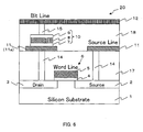
- Fig. 6 shows a schematic diagram of a cross section of the memory cell 20 that forms the memory array 101.
- the memory cell 20 is formed of: a source region 2 and a drain region 3 that have been formed on a semiconductor substrate 1; a selective transistor 6 made of a gate electrode 5 that has been formed on a gate oxide film 4; and a variable resistive element 10 where a variable resistor 8 of which the resistive value changes depending on an applied voltage is placed between a lower electrode 7 and an upper electrode 9, wherein the drain region 3 and the lower electrode 7 are electrically connected in series.
- variable resistive element 10 is formed in the same manner as the single variable resistive element 10 shown in Fig. 1. This memory cell configuration differs from that illustrated in Fig. 3 in the way that the single memory cell is formed of one variable resistive element 10.
- the number of the variable resistive elements 10 arranged within one memory cell may be determined in accordance with the characteristics and functions of the entire configuration of the memory device.
- Fig. 7 schematically shows an example of the configuration of the memory array 101.
- the memory array 101 has m ⁇ n memory cells 20 at intersections of m bit lines (BL1 to BLm) and n word lines (WL1 to WLn).
- n source lines (SL1 to SLn) are placed in parallel to the word lines in the configuration.
- the configuration of the memory array 101 is not limited to that of Fig. 7.
- a memory cell 20 is formed of a series circuit of a selective transistor 6 and a variable resistive element 10 and thereby, the selective transistor 6 of the memory cell 20, which is selected by the potential of a word line, is turned ON and in addition, a program or erasure voltage is selectively applied to only the variable resistive element 10 of the memory cell 20 which has been selected by the potential of a bit line, and thereby, the resistance value of the variable resistor 8 in the variable resistive element 10 is changed in the configuration.
- the block configuration that includes the peripheral circuits of the inventive device 100 shown in Fig. 5 is the same as or similar to the block configuration of a general nonvolatile semiconductor memory device.
- the each circuit blocks are briefly described below.
- Information is stored in a specific memory cell within the memory array 101 that corresponds to the address that has been inputted from the address line 102 and this information passes through the data line 103 so as to be outputted to an external device.
- a word line decoder 104 selects a word line of the memory array 101 which corresponds to the signal that has been inputted to the address line 102 and a bit line decoder 105 selects a bit line of the memory array 101 which corresponds to the address signal that has been inputted to the address line 102 and furthermore, a source line decoder 106 selects a source line of the memory array 101 which corresponds to the address signal that has been inputted to the address line 102.
- a control circuit 108 controls program, erasure and readout of the memory array 101.
- the control circuit 108 controls readout, program and erasure operations of the word line decoder 104, the bit line decoder 105, the source line decoder 106, the voltage switching circuit 109 and the memory array 101 based on the address signal that has been inputted from the address line 102, the data input (at the time of program) that has been inputted from the data line 103 and control input signal that has been inputted from the control signal line 110.
- the control circuit 108 has functions as a general address buffer circuit, a data input/output buffer circuit and a control input buffer circuit (not shown).
- the voltage switching circuit 109 supplies voltages to a word line, a bit line and a source line which are required at the time of readout, program and erasure of the memory array 101.
- Vcc indicates a supply voltage to the device
- Vss indicates a ground voltage
- Vpp indicates a voltage for program and erasure.
- data readout is carried out through the bit line decoder 105 and the readout circuit 107 from the memory array 101.
- the readout circuit 107 determines the condition of data and this result is sent to the control circuit 108 so as to be outputted to the data line 103.
- the block configuration of the inventive device 100 and the configuration of a memory cell illustrated in Fig. 5 are examples and can appropriately be modified in accordance with the characteristics and the like of the variable resistive element 10.
- the memory cell 20 may be formed of a single variable resistive element 10 instead of being formed of a series circuit of the selective transistor 6 and the variable resistive element 10.
- a selective diode may be used in place of the selective transistor 6.
Landscapes
- Engineering & Computer Science (AREA)
- Chemical & Material Sciences (AREA)
- Materials Engineering (AREA)
- Manufacturing & Machinery (AREA)
- Semiconductor Memories (AREA)
Applications Claiming Priority (2)
| Application Number | Priority Date | Filing Date | Title |
|---|---|---|---|
| JP2004004949 | 2004-01-13 | ||
| JP2004004949A JP2005203389A (ja) | 2004-01-13 | 2004-01-13 | 不揮発性半導体記憶装置の製造方法 |
Publications (2)
| Publication Number | Publication Date |
|---|---|
| EP1555700A2 true EP1555700A2 (de) | 2005-07-20 |
| EP1555700A3 EP1555700A3 (de) | 2007-10-03 |
Family
ID=34616828
Family Applications (1)
| Application Number | Title | Priority Date | Filing Date |
|---|---|---|---|
| EP05000519A Withdrawn EP1555700A3 (de) | 2004-01-13 | 2005-01-12 | Verfahren zur Herstellung einer nichtflüchtigen Speichervorrichtung mit einem variablen Widerstand |
Country Status (6)
| Country | Link |
|---|---|
| US (1) | US20050153504A1 (de) |
| EP (1) | EP1555700A3 (de) |
| JP (1) | JP2005203389A (de) |
| KR (1) | KR100672272B1 (de) |
| CN (1) | CN1641880A (de) |
| TW (1) | TWI254447B (de) |
Cited By (2)
| Publication number | Priority date | Publication date | Assignee | Title |
|---|---|---|---|---|
| EP2099071A4 (de) * | 2006-12-19 | 2011-01-19 | Fujitsu Ltd | Widerstandsänderungseinrichtung und prozess zu ihrer herstellung |
| EP2099070B1 (de) * | 2006-12-19 | 2012-09-26 | Fujitsu Limited | Prozess zur herstellung eines widerstandsänderungsbauelements |
Families Citing this family (33)
| Publication number | Priority date | Publication date | Assignee | Title |
|---|---|---|---|---|
| JP2004273656A (ja) * | 2003-03-07 | 2004-09-30 | Taiyo Yuden Co Ltd | Epir素子及びそれを利用した半導体装置 |
| JP2006022401A (ja) * | 2004-05-27 | 2006-01-26 | Sharp Corp | Cmr薄膜の形成方法 |
| KR100576369B1 (ko) * | 2004-11-23 | 2006-05-03 | 삼성전자주식회사 | 전이 금속 산화막을 데이타 저장 물질막으로 채택하는비휘발성 기억소자의 프로그램 방법 |
| US7521705B2 (en) | 2005-08-15 | 2009-04-21 | Micron Technology, Inc. | Reproducible resistance variable insulating memory devices having a shaped bottom electrode |
| JP5049491B2 (ja) * | 2005-12-22 | 2012-10-17 | パナソニック株式会社 | 電気素子,メモリ装置,および半導体集積回路 |
| US7362608B2 (en) * | 2006-03-02 | 2008-04-22 | Infineon Technologies Ag | Phase change memory fabricated using self-aligned processing |
| US20070205096A1 (en) * | 2006-03-06 | 2007-09-06 | Makoto Nagashima | Magnetron based wafer processing |
| US8395199B2 (en) | 2006-03-25 | 2013-03-12 | 4D-S Pty Ltd. | Systems and methods for fabricating self-aligned memory cell |
| KR100785021B1 (ko) * | 2006-06-13 | 2007-12-11 | 삼성전자주식회사 | Cu2O를 포함한 비휘발성 가변 저항 메모리 소자 |
| US8454810B2 (en) | 2006-07-14 | 2013-06-04 | 4D-S Pty Ltd. | Dual hexagonal shaped plasma source |
| US7932548B2 (en) * | 2006-07-14 | 2011-04-26 | 4D-S Pty Ltd. | Systems and methods for fabricating self-aligned memory cell |
| US8308915B2 (en) | 2006-09-14 | 2012-11-13 | 4D-S Pty Ltd. | Systems and methods for magnetron deposition |
| KR100781982B1 (ko) * | 2006-11-02 | 2007-12-06 | 삼성전자주식회사 | 반도체 메모리 장치 및 워드라인 콘택들의 레이아웃 구조 |
| JP5062181B2 (ja) * | 2006-12-19 | 2012-10-31 | 富士通株式会社 | 抵抗変化素子及びその製造方法 |
| WO2008075412A1 (ja) * | 2006-12-19 | 2008-06-26 | Fujitsu Limited | 抵抗変化素子及びその製造方法 |
| KR100802076B1 (ko) | 2006-12-27 | 2008-02-12 | 주식회사 하이닉스반도체 | 비휘발성 메모리 소자 및 그 제조방법 |
| KR101313784B1 (ko) | 2007-01-12 | 2013-10-01 | 삼성전자주식회사 | 저항성 메모리 소자 및 그 제조방법 |
| KR100969153B1 (ko) * | 2008-04-11 | 2010-07-08 | 광주과학기술원 | 비휘발성 저항변화 메모리 소자 |
| US20090267042A1 (en) * | 2008-04-24 | 2009-10-29 | Happ Thomas D | Integrated Circuit and Method of Manufacturing an Integrated Circuit |
| US8004874B2 (en) * | 2008-08-06 | 2011-08-23 | Seagate Technology Llc | Multi-terminal resistance device |
| US7615459B1 (en) * | 2008-08-12 | 2009-11-10 | Sharp Kabushiki Kaisha | Manufacturing method for variable resistive element |
| KR101486984B1 (ko) * | 2008-10-30 | 2015-01-30 | 삼성전자주식회사 | 가변 저항 메모리 소자 및 그 형성방법 |
| TWI473209B (zh) | 2009-12-09 | 2015-02-11 | Univ Nat Taiwan Science Tech | 電阻式記憶體的製造方法 |
| US9679686B2 (en) * | 2011-12-23 | 2017-06-13 | Intel Corporation | Process tunable resistor with user selectable values |
| US8847187B2 (en) * | 2012-12-03 | 2014-09-30 | Intermolecular, Inc. | Method of forming anneal-resistant embedded resistor for non-volatile memory application |
| TWI513074B (zh) * | 2013-01-08 | 2015-12-11 | Nat Univ Tsing Hua | 電阻式記憶體 |
| US20140264224A1 (en) | 2013-03-14 | 2014-09-18 | Intermolecular, Inc. | Performance Enhancement of Forming-Free ReRAM Devices Using 3D Nanoparticles |
| US9245925B1 (en) * | 2015-01-15 | 2016-01-26 | Macronix International Co., Ltd. | RRAM process with metal protection layer |
| US9444464B1 (en) * | 2015-03-12 | 2016-09-13 | Microsemi SoC Corporation | Compact ReRAM based FPGA |
| JP6430576B2 (ja) * | 2017-04-19 | 2018-11-28 | ウィンボンド エレクトロニクス コーポレーション | 抵抗変化型ランダムアクセスメモリ |
| JP6829733B2 (ja) * | 2019-01-16 | 2021-02-10 | ウィンボンド エレクトロニクス コーポレーション | 抵抗変化型ランダムアクセスメモリ |
| CN111668371B (zh) * | 2020-04-30 | 2024-01-26 | 陕西科技大学 | 化学气相沉积制备基于无铅全无机钙钛矿薄膜的柔性阻变存储器 |
| US20240413111A1 (en) * | 2023-06-07 | 2024-12-12 | Bae Systems Information And Electronic Systems Integration Inc. | Inline resistor integrated with conductive contact pad structure |
Family Cites Families (10)
| Publication number | Priority date | Publication date | Assignee | Title |
|---|---|---|---|---|
| JP3360350B2 (ja) * | 1993-04-21 | 2002-12-24 | ヤマハ株式会社 | 表面平坦化法 |
| US5566045A (en) * | 1994-08-01 | 1996-10-15 | Texas Instruments, Inc. | High-dielectric-constant material electrodes comprising thin platinum layers |
| US6117784A (en) * | 1997-11-12 | 2000-09-12 | International Business Machines Corporation | Process for integrated circuit wiring |
| US6204139B1 (en) * | 1998-08-25 | 2001-03-20 | University Of Houston | Method for switching the properties of perovskite materials used in thin film resistors |
| US6368967B1 (en) * | 2000-05-04 | 2002-04-09 | Advanced Micro Devices, Inc. | Method to control mechanical stress of copper interconnect line using post-plating copper anneal |
| JP3677455B2 (ja) * | 2001-02-13 | 2005-08-03 | Necエレクトロニクス株式会社 | 不揮発性磁気記憶装置およびその製造方法 |
| US6759249B2 (en) * | 2002-02-07 | 2004-07-06 | Sharp Laboratories Of America, Inc. | Device and method for reversible resistance change induced by electric pulses in non-crystalline perovskite unipolar programmable memory |
| US6917532B2 (en) * | 2002-06-21 | 2005-07-12 | Hewlett-Packard Development Company, L.P. | Memory storage device with segmented column line array |
| US6583003B1 (en) * | 2002-09-26 | 2003-06-24 | Sharp Laboratories Of America, Inc. | Method of fabricating 1T1R resistive memory array |
| US7063984B2 (en) * | 2003-03-13 | 2006-06-20 | Unity Semiconductor Corporation | Low temperature deposition of complex metal oxides (CMO) memory materials for non-volatile memory integrated circuits |
-
2004
- 2004-01-13 JP JP2004004949A patent/JP2005203389A/ja active Pending
- 2004-12-20 TW TW093139659A patent/TWI254447B/zh not_active IP Right Cessation
-
2005
- 2005-01-12 EP EP05000519A patent/EP1555700A3/de not_active Withdrawn
- 2005-01-12 US US11/035,089 patent/US20050153504A1/en not_active Abandoned
- 2005-01-12 KR KR1020050003022A patent/KR100672272B1/ko not_active Expired - Fee Related
- 2005-01-13 CN CNA2005100057231A patent/CN1641880A/zh active Pending
Cited By (4)
| Publication number | Priority date | Publication date | Assignee | Title |
|---|---|---|---|---|
| EP2099071A4 (de) * | 2006-12-19 | 2011-01-19 | Fujitsu Ltd | Widerstandsänderungseinrichtung und prozess zu ihrer herstellung |
| US8106377B2 (en) | 2006-12-19 | 2012-01-31 | Fujitsu Limited | Resistance change element and method of manufacturing the same |
| EP2099070B1 (de) * | 2006-12-19 | 2012-09-26 | Fujitsu Limited | Prozess zur herstellung eines widerstandsänderungsbauelements |
| US8533938B2 (en) | 2006-12-19 | 2013-09-17 | Fujitsu Limited | Method of manufacturing resistance change element |
Also Published As
| Publication number | Publication date |
|---|---|
| KR20050074328A (ko) | 2005-07-18 |
| TW200532898A (en) | 2005-10-01 |
| TWI254447B (en) | 2006-05-01 |
| EP1555700A3 (de) | 2007-10-03 |
| US20050153504A1 (en) | 2005-07-14 |
| KR100672272B1 (ko) | 2007-01-24 |
| CN1641880A (zh) | 2005-07-20 |
| JP2005203389A (ja) | 2005-07-28 |
Similar Documents
| Publication | Publication Date | Title |
|---|---|---|
| US7259387B2 (en) | Nonvolatile semiconductor memory device | |
| EP1555700A2 (de) | Verfahren zur Herstellung einer nichtflüchtigen Speichervorrichtung mit einem variablen Widerstand | |
| US11502249B2 (en) | Memory element with a reactive metal layer | |
| US10644069B2 (en) | Memory devices having crosspoint memory arrays therein with multi-level word line and bit line structures | |
| US7042035B2 (en) | Memory array with high temperature wiring | |
| US7400006B1 (en) | Conductive memory device with conductive oxide electrodes | |
| JP3889023B2 (ja) | 可変抵抗素子とその製造方法並びにそれを備えた記憶装置 | |
| KR100769538B1 (ko) | 가변저항소자의 구동방법 및 기억장치 | |
| US7067862B2 (en) | Conductive memory device with conductive oxide electrodes | |
| US6856536B2 (en) | Non-volatile memory with a single transistor and resistive memory element | |
| US7045840B2 (en) | Nonvolatile semiconductor memory device comprising a variable resistive element containing a perovskite-type crystal structure | |
| US7233017B2 (en) | Multibit phase change memory device and method of driving the same | |
| JP4939414B2 (ja) | 可変抵抗素子 | |
| WO2007055071A1 (ja) | 可変抵抗素子を備えた不揮発性半導体記憶装置の製造方法 |
Legal Events
| Date | Code | Title | Description |
|---|---|---|---|
| PUAI | Public reference made under article 153(3) epc to a published international application that has entered the european phase |
Free format text: ORIGINAL CODE: 0009012 |
|
| AK | Designated contracting states |
Kind code of ref document: A2 Designated state(s): AT BE BG CH CY CZ DE DK EE ES FI FR GB GR HU IE IS IT LI LT LU MC NL PL PT RO SE SI SK TR |
|
| AX | Request for extension of the european patent |
Extension state: AL BA HR LV MK YU |
|
| PUAL | Search report despatched |
Free format text: ORIGINAL CODE: 0009013 |
|
| AK | Designated contracting states |
Kind code of ref document: A3 Designated state(s): AT BE BG CH CY CZ DE DK EE ES FI FR GB GR HU IE IS IT LI LT LU MC NL PL PT RO SE SI SK TR |
|
| AX | Request for extension of the european patent |
Extension state: AL BA HR LV MK YU |
|
| RIC1 | Information provided on ipc code assigned before grant |
Ipc: H01L 27/06 20060101ALI20070829BHEP Ipc: H01L 27/112 20060101ALI20070829BHEP Ipc: H01L 21/8246 20060101ALI20070829BHEP Ipc: H01L 29/68 20060101ALI20070829BHEP Ipc: H01L 45/00 20060101AFI20050406BHEP |
|
| 17P | Request for examination filed |
Effective date: 20080319 |
|
| 17Q | First examination report despatched |
Effective date: 20080422 |
|
| AKX | Designation fees paid |
Designated state(s): DE FR GB IT |
|
| STAA | Information on the status of an ep patent application or granted ep patent |
Free format text: STATUS: THE APPLICATION IS DEEMED TO BE WITHDRAWN |
|
| 18D | Application deemed to be withdrawn |
Effective date: 20080903 |