Technical Field
The present invention relates to an information
processing apparatus and an information storing apparatus
such as memories or other devices operating on a
predetermined synchronizing clock signal being supplied,
as well as an information processing method and an
information processing program for use with such
apparatuses. More particularly, the invention relates to
an information processing apparatus, an information
storing apparatus, an information processing method, and
an information processing program for implementing
optimal signal processing operations when the
synchronizing clock signal in use is varied in frequency.
Background Art
Recent years have witnessed widespread use of
electronic devices such as personal computers and PDAs
(personal digital assistants) containing a plurality of
LSIs (large-scale integrated circuits) in their system
configuration. The signals used by these LSIs are input,
output, and processed using synchronizing clock signals.
Generally, a device that operates on a synchronizing
clock signal is structured so that the speed of its
performance is proportional to the frequency of the clock
signal. Typical devices operating on the synchronizing
clock signal include CPUs (Central Processing Units),
memories, and north bridges.
Also known today are devices acting on variable,
not fixed operating frequencies. Many electronic devices
such as personal computers, PDAs and cellular phones are
designed to operate only as needed. In more and more
systems, their operating frequency is lowered in standby
mode or in sleep mode in order to attain a reduced level
of power dissipation; when a call is being made or moving
picture signals are being processed, the operating
frequency is raised to accelerate the processing of the
systems. (One such system is disclosed illustratively in
Japanese Patent Laid-open No. 2000-163965.)
These systems with their operating frequencies made
variable usually have their functional parts divided in
two regions. One region for which the operating frequency
must remain fixed is isolated from the other region fed
with a clock signal at variable frequencies. This
structure is intended to prevent the region of the parts
operating at variable frequencies from adversely
affecting the other region of fixed-frequency parts.
Meanwhile, the information processing apparatuses
using a synchronizing signal at varied frequencies are
required to provide steady performance regardless of
their synchronizing signal being fixed or variable.
Generally, if an apparatus is guaranteed to operate at a
high frequency, i.e., at short clock intervals, the
apparatus will also operate at reduced frequencies but
the performance of its signal processing will be lowered
in proportion to the drop in frequency. Although the
dissipation of power is curtailed by simply reducing the
operating speed in keeping with the lowered clock
frequency, that is not an optimally controlled operating
state. A more sophisticated control scheme has been
called for.
The present invention has been made in view of the
aforementioned technical problems and provides an
information processing apparatus, an information storing
apparatus, an information processing method, and an
information processing program for implementing an
optimal signal processing setup that ensures steady
performance using variable operating frequencies.
Disclosure of Invention
In solving the foregoing and other technical
problems and according to one aspect of the invention,
there is provided an information processing apparatus
including: a frequency information operating section for
operating on frequency information about a synchronizing
clock signal having a variable frequency; and an
information processing section which is supplied with the
synchronizing clock signal as an operating clock signal
and which performs information processing in suitably
timed relation with results of the operation by the
frequency information operating section.
Where the information processing apparatus above of
the invention is in use, the frequency information
operating section of the apparatus admits frequency
information about a synchronizing clock signal having a
variable frequency and carries out such operations as
adding up the frequency information or decoding the
frequency information in encoded form. The information
processing section of the apparatus performs information
processing in accordance with the result of such
operations. Having acquired the frequency information,
the information processing section can proceed with its
processing in optimal fashion in a manner eliminating
wasteful latency times.
According to another aspect of the invention, there
is provided an information storing apparatus including: a
frequency information operating section for operating on
frequency information about a synchronizing clock signal
having a variable frequency; and an information storing
section which is supplied with the synchronizing clock
signal as an operating clock signal and which performs an
information storing operation in suitably timed relation
with results of the operation by the frequency
information operating section.
Where the information storing apparatus above of
the invention is in use, the frequency information
operating section of the apparatus similarly admits
frequency information about a synchronizing clock signal
having a variable frequency and carries out such
operations as adding up the frequency information or
decoding the frequency information in encoded form. The
result of such operations is used by the inventive
information storing apparatus as the basis for optimally
storing information also in a manner eliminating wasteful
latency times.
Brief Description of Drawings
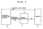
Fig. 1 is a block diagram of an information
processing apparatus embodying this invention.
Figs. 2A, 2B and 2C are timing charts in effect
when a memory device is in operation, Fig. 2A showing how
the device is timed to operate on a fixed-frequency clock
signal, Fig. 2B depicting how the device operates in
fixedly timed fashion on a variable clock frequency
signal, Fig. 2C illustrating how the device operates in
suitably timed relation with results from calculations of
frequency information.
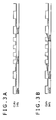
Figs. 3A and 3B are timing charts indicating
examples of frequency information being used, Fig. 3A
showing an example in which the frequency information
denotes the frequency of a current operating clock signal
CLKv, Fig. 3B depicting an example in which the frequency
information is indexed to the frequency of the next clock
interval preceding changes in the frequency of the
operating clock signal CLKv.
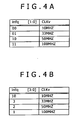
Figs. 4A and 4B are tabular views showing examples
of how frequency information is encoded, Fig. 4A showing
an example in which the information is encoded in two
bits, Fig. 4B illustrating an example in which the
information is encoded using cyclically proportional
values.
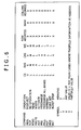
Fig. 5 is a block diagram of an information
processing apparatus built to embody the invention by use
of a memory controller and an SDRAM.
Fig. 6 is a tabular view constituting a table of
signal-to-command correspondence applicable to the SDRAM
in Fig. 5.
Fig. 7 is a block diagram of an information
processing apparatus built to embody the invention by
incorporating a memory controller and a memory into a PDA.
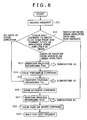
Fig. 8 is a flowchart of steps constituting an
information processing method according to the invention,
the steps being carried out by determining whether there
is a match between data and an address in a sense
amplifier for the SDRAM.
Fig. 9 is a flowchart of steps constituting a
subroutine as part of the inventive information
processing method, the subroutine calculating a wait time
based on frequency information.
Figs. 10A and 10B are timing charts applicable to
another information processing method according to the
invention and for use with the inventive information
processing apparatus.
Best Mode for Carrying out the Invention
A memory device practiced as an information storing
apparatus for use with an information processing
apparatus according to the invention will now be
described with reference to the accompanying drawings.
The memory device embodying the invention primarily
includes a memory 11 made of an SDRAM (Synchronous
Dynamic Random Access Memory), a memory controller 12 for
controlling the memory 11, and a frequency controlling
section 13 for outputting frequency information Infq.
The memory 11 of this embodiment is an SDRAM which,
given a read start address, outputs data in synchronism
with a clock signal CLKv at a relatively high speed. The
clock signal CLKv for this embodiment is variable in
frequency. Illustratively, clock frequencies such as 10
MHz, 33 MHz, 50 MHz, 100 MHz and 133 MHz are switched
over in keeping with the state of the information
processing apparatus or of an electronic device in which
this information processing apparatus is installed. The
variable clock signal CLKv may alternatively be a so-called
base clock, i.e., a clock signal external to the
CPU of the system, or a clock signal generated solely for
control of the memory 11. The variable clock signal CLKv
is output by the frequency controlling section 13.
Alternatively, the clock signal CLKv may be supplied
directly from a separately furnished frequency generation
circuit. The memory 11, to be described later in
structural terms, may be formed by a two-chip arrangement
in which the memory 11 and the memory controller 12 are
mounted on a different chip each. The memory 11 may be
furnished as a memory core and included in the same chip
as the memory controller 12. The memory 11 is supplied
with the variable clock signal CLKv as well as with a
control signal Sig from the memory controller 12.
Furthermore, signal lines, not shown, which carry a row
address, a column address and data being input and output
are connected to the memory 11. Although the memory 11 of
this embodiment is an SDRAM, this is not limitative of
the invention. Alternatively, although the memory 11 is a
synchronous DRAM, it may be an ordinary DRAM, a first-page
DRAM, an EDODRAM (Extended Data Out Dynamic Random
Access Memory), a DDRSDRAM (Double Data Rate Synchronous
Dynamic Random Access Memory), or a DRDRAM (Direct Rambus
Dynamic Random Access Memory). The memory 11 is not
limited to the DRAM category; it may be an SRAM (Static
Random Access Memory), a ROM (Read-Only Memory), or a
flash memory. The memory device or information processing
apparatus including the memory according to this
invention may be a microcomputer or some other signal
processing chip incorporating a memory unit.
The memory controller 12 is a device that outputs
the control signal Sig for controlling the memory 11 in
operation. The control signal Sig generically refers to a
group of signals including CS (chip select), RAS (row
address strobe), CAS (column address strobe), WE (write
enable), and CKE. The memory controller 12 is also
supplied with the variable clock signal CLKv and
synchronizes the control signal Sig with the supplied
clock signal CLKv in output timing. In addition, the
memory controller 12 admits frequency information Infq
from the frequency controlling section 13 that includes
frequency information about the clock signal CLKv. The
frequency information Infq may be information about the
current clock signal CLKv or may be information about a
temporally ensuing clock signal CLKv. The frequency
information Infq is typically provided in encoded form.
An example of the coding will be discussed later.
Alternatively the frequency information Infq may be
information about the variable clock signal CLKv itself
or about a linearly transformed variation of the signal.
The memory controller 12 performs its operation by use of
the input frequency information Infq, optimally
controlling the memory 11 in a manner reflecting the
result of the operation as will be discussed later.
The frequency controlling section 13 is a circuit
that outputs the frequency information Infq. With this
embodiment, the frequency controlling section 13 also
outputs the variable clock signal CLKv. The frequency
controlling section 13 is so structured as to vary the
generated clock signal CLKv in frequency in response to
commands from the CPU. Illustratively, the frequency
controlling section 13 can reduce its operating clock
frequency in soft off mode, standby mode, or sleep mode
in order to lower the level of power dissipation. The
frequency controlling section 13 may be in the same chip
as the memory 11 or as the controller 12, or may be
furnished in a separate chip.
Figs. 2A, 2B and 2C are timing charts in effect
when the memory device of this embodiment is in operation.
Fig. 2A shows how a read operation is performed on the
memory 11 using a clock signal fixed at a frequency of
100 MHz. Fig. 2B depicts by way of comparison how the
read operation on the memory 11 is carried out in fixedly
timed fashion on a variable clock frequency signal. Fig.
2C illustrates how the same read operation is executed in
suitably timed relation with results from calculations of
frequency information. Throughout the three timing charts,
the symbol CLK stands for a fixed clock signal and CLKv
for a variable clock signal. In the command signal part,
reference character "A" stands for the period in which an
activate operation command is issued, "R" for the period
in which a read operation command is issued, and "P" for
the period in which a precharge operation command is
issued.
Control over an SDRAM generally involves a number
of parameters: Tras (RAS activate time) denoting the time
period ranging from an activate operation to a precharge
operation, Trcd (RAS-CAS delay time) representing the
time period from an activate operation to a read
operation, and Trp (precharge time) indicating the time
period from a precharge operation to an activate
operation. To issue any one of the above commands
requires at least waiting for the corresponding time
period to elapse. In case of a failure to observe the
time period, the corresponding memory operation can
become unpredictable.
Before operations by this embodiment in keeping
with a clock signal of a variable frequency are explained,
a brief description will be made of a case where the
clock signal has a fixed frequency for comparison. As
long as the operating clock signal is fixed at a
predetermined frequency, optimization of the operations
is relatively easy. That is, if an operation is made
using the clock signal fixed at the frequency of 100 MHz
as shown in Fig. 2A, the time parameters {Tras, Trcd,
Trp} for this SDRAM are {40 ns, 20 ns, 20 ns}; if the CAS
latency is 2, then the RAS activate time Tras is 4 clock
intervals long, RAS-CAS delay time Trcd is 2 clock
intervals long, and the precharge time Trp is 2 clock
intervals long in latency. With these parameters in place,
the operations are optimized at the fixed frequency of
100 MHz.
By contrast, when the operating clock signal is
varied in frequency with the fixed-frequency control
setup still in place, latency times occur in low
frequency regions where each clock interval is prolonged.
These latency times, when added up, can worsen the
overall performance of the device. As shown in Fig. 2B,
the first RAS activate time Tras with a leading edge at
which the "A" command is issued remains four clock
intervals long. Because the setup of Fig. 2B applies to a
clock frequency of 50 MHz, half of the initial 100 MHz,
the RAS activate time Tras is in fact 2 clock intervals
longer than if the frequency of 100 MHz is in effect,
with the necessary wait time having already elapsed. The
RAS activate time Tras for the next activate operation
("A") is 3 clock intervals longer than if the frequency
of 100 MHz is in use. In like manner, the RAS-CAS delay
time Trcd and the precharge time Trp involve prolonged
latency times depending on the changes in the operating
clock frequency.
The memory device of this embodiment performs its
operation properly using the frequency information Infq
when the operating clock signal is varied in frequency.
As indicated in Fig. 2C, the signal processing is carried
out in keeping with the frequency being used. The memory
controller 12 is fed with the frequency information Infq
from the frequency controlling section 13 as shown in Fig.
1. Given the frequency information Infq, the memory
controller 12 calculates the clock signal period
accordingly. If any command is found likely to be delayed
when issued, the memory controller 12 causes the command
in question to be issued earlier than usual for the
memory 13 so that the latency time involved will be
minimal. More specifically, as shown in Fig. 2C, the
memory controller 12 receives from the frequency
controlling section 13 the frequency information Infq
saying that the clock frequency is 50 MHz after the
activate operation ("A") command is issued. The
information is received at least one clock interval
earlier than the time at which a read ("R") command is to
be issued. Based on the received frequency information
Infq, a clock pulse is first generated to give the timing
for issuing the activate operation ("A") command,
followed immediately by a clock pulse to give the timing
for issuing the next read operation ("R") command. If the
memory device of this embodiment were not used, the pulse
to give the timing for issuing the read operation ("R")
command would be 1 clock interval apart from the
preceding interval as shown in Fig. 2A or 2B. With the
memory device of this embodiment, by contrast, the memory
controller 12 having received the frequency information
Infq beforehand from the frequency controlling section 13
recognizes that the necessary operations are guaranteed
even if pulses are generated consecutively to give the
timing for issuing the activate operation ("A") command
and the next read operation ("R") command. This allows
the memory controller 12 optimally to control the memory
11 so that wasteful latency times are eliminated and
overall performance is enhanced.
The memory controller can issue the read operation
("R") command on the condition that the RAS-CAS delay
time Trcd be met. The RAS-CAS delay time is a necessary
wait time based on the frequency information Infq at
least for the period from the time the issuance of the
activate operation ("A") command has ended until the
issuance of the next read operation ("R") command has
ended. With the clock frequency assumed to be 100 MHz
during issuance of the read operation ("R") command, the
memory controller 12 can issue the read operation ("R")
command on the condition that the RAS-CAS delay time Trcd
as the required wait time be met, on the basis of the
frequency information Infq in effect until the read
operation ("R") command is issued.
Likewise, the memory controller based on the
frequency information Infq issues the activate operation
("A") command and precharge operation ("P") command in
such a manner that the necessary wait time is met and
that the precharge time Trp and the RAS activate time
Tras are optimally shortened.
What follows is a more detailed description of how
the memory controller 12 recognizes beforehand that the
necessary operations are guaranteed. In the setup of Fig.
2C, the second clock pulse is recognized to be 50 MHz and
the clock interval is calculated at 20 ns based on the
frequency information Infq. The RAS-CAS delay time Trcd
here is 20 ns for this SDRAM, so that the clock period of
20 ns is satisfactory. Thus the memory controller 12
generates clock pulses consecutively to give the timing
for issuing the activate operation ("A") command and the
next read operation ("R") command. The successive
issuance of the commands minimizes latency times and
contributes to speeding up overall performance.
Referring to Figs. 3A through 4B, the frequency
information Infq will now be described in more detail.
Illustratively, the frequency information Infq may be
data bits indexed to the frequency of the variable clock
signal CLKv. The frequency information Infq may be
indexed to the current frequency of the operating clock
signal CLKv as shown in Fig. 3A, or to the next clock
interval preceding changes in the frequency of the
operating clock signal CLKv as depicted in Fig. 3B. The
frequency information Infq may alternatively be indexed
solely to the points of change in the frequency, not
shown. As another alternative, the frequency information
Infq may be indexed not only to the next clock frequency
but also to the frequency occurring a predetermined
plurality of clock intervals later than usual.
The clock frequency is indexed illustratively by
decoding the frequency information Infq in encoded form.
Figs. 4A and 4B show two encoding methods in tabular form,
which are only examples and not limitative of the
invention. The encoding method of Fig. 4A involves
assigning two-bit data to each of the variable
frequencies of the clock signal CLKv. In this example,
data {00} is assigned to the frequency of 10 MHz, data
{01} to the frequency of 33 MHz, {10} to 50 MHz, and {11}
to 100 MHz. According to this encoding method, the data
length remains 2 bits even when the clock signal
frequency is changed from 10 MHz to 100 MHz, i.e., a
tenfold increase in frequency. This means that
complicated processing steps for circuit arrangements are
not needed for decoding the data.
The encoding method of Fig. 4B involves assigning
to the variable clock signal CLKv the reciprocal of each
of its varied frequencies. The reciprocal of a frequency
of the clock signal CLKv corresponds to a single clock
interval for that frequency. In this example, data {10}
is assigned to the frequency of 10 MHz for the clock
signal CLKv, data {3} to the frequency of 33 MHz, {2} to
50 MHz, and {1} to 100 MHz. Since each value of these
data items corresponds by itself to the single clock
interval, wait times are determined by simple
multiplications. That is, when the frequencies of the
clock signal CLKv are 10 MHz, 33 MHz, 50 MHz, and 100 MHz,
the clock periods are 100 ns, 30 ns, 20 ns, and 10 ns,
respectively. The periods are easy to determine through
multiplication of the respective data values by 10 ns.
Referring now to Figs. 5 and 6, the memory device
of this embodiment is described below in more detail. Fig.
5 shows a memory controller 30 and a memory unit 31. With
this embodiment, the memory controller 30 is supplied
with the frequency information Infq and operates in
optimal fashion when the operating clock signal is varied
in frequency.
The memory controller 30 first receives the
frequency information Infq from the frequency controlling
section as described above in order to issue commands in
a suitably timed manner. Fig. 6 is a typical signal-to-command
correspondence table for use with this memory
device. In the table, bar symbols are omitted for
simplification. When the CS (chip select) signal is
brought "L" ("Low" level), the memory unit 31 is selected.
As mentioned above, the activate operation ("A") command,
read operation ("R") command, and precharge operation
("P") command are each formed by suitably combining the
control signals RAS (row address strobe), CAS (column
address strobe), and WE (write enable). More specifically,
the activate operation command is formed by driving the
RAS signal Low, the CAS signal High, and the WE signal
High; the read operation command is formed by bringing
the RAS signal High, the CAS signal Low, and the WE
signal High; the write operation command is formed by
driving the RAS signal High, the CAS signal Low, and the
WE signal Low; and the precharge operation command is
formed by bringing the RAS signal Low, the CAS signal
High, and the WE signal Low. Suppose now that with the
clock signal CLKv varied in frequency as described above,
the activate operation command and the read operation
command are issued consecutively as indicated by the
second clock interval in Fig. 2C. In such a case, all
that needs to be done is to drive the RAS signal from Low
to High and the CAS signal from High to Low. The signal
level shifts are carried out through calculations based
on the frequency information Infq from the frequency
controlling section.
The memory unit 31 is made up of a memory bank 55,
a sense amplifier 56 for amplifying the electrical
charges in each of the cells in the memory bank 55, and
other peripheral circuits. The memory bank 55 is a part
that actually accommodates data and is constituted by a
plurality of cells 55a. Each cell 55a is a capacitor in
structure and, depending on the data to be stored therein,
is either charged or discharged electrically. Data is
stored in the memory bank 55 in the form of charged
patterns constructed by the cells 55a. In this example,
eight by eight cells 55a are provided in a single memory
bank 55. Needless to say, the number of cells 55a may be
larger or smaller than that as needed.
The group of cells 55a on each row of the cells in
the memory bank 55 is specifically called a page 55b.
When supplied with a refresh signal from a refresh timing
generator of a refresh control circuit, not shown, or
with a read signal from a row selector 53, the memory
bank 55 transfers to the sense amplifier 56 the
electrical charges from each of the cells 55a in a unit
of the pages 55b corresponding to the rows to which the
signal in question is applied. In Fig. 3, the numbers (0
to 7) marked vertically and horizontally around the
memory bank 55 indicate the rows in the vertical
direction and the columns in the horizontal direction.
The sense amplifier 56 receives the data
transferred from the cells 55a on the page 55b designated
by the row selector 53, amplifies the data up to a
predetermined potential level, and sends the amplified
data back to the originating page 55b. If, with the cells
being charged, a read signal is input from a column
selector 57 designating a column of cells, then the sense
amplifier 56 reads the data from the designated column
and outputs the retrieved data to an output amplifier 58.
In Fig. 5, the sense amplifier 56 is so structured
as to amplify only the electrical charge in the cells 55a
of one page 55b at a time. This structure permits refresh
or read processing only on a page-by-page basis. For this
reason, the CPU, not shown, provides control so that the
refresh signal generated by the self-refresh timing
generator or the read signal generated by the row
selector 53 is timed to execute the corresponding
operation on one row at a time. Alternatively, a
plurality of sense amplifiers 56 may be provided to carry
out refresh or read operations parallelly on a plurality
of pages (i.e., rows).
A column address latch 52 is activated upon receipt
of the CAS signal from the memory controller 30,
outputting to the column selector 57 column address
information pointing to the location of a column of cells
55a in the memory bank 55. Given the column information
from the column address latch 52, the column selector 57
outputs to the sense amplifier 56 a data read signal
corresponding to the designated column, and causes the
sense amplifier 56 to output its data to the output
amplifier 58. The output amplifier 58 amplifies the input
electrical charge in order to output the retrieved data
to the CPU through the memory controller 30.
Below is a description of how the memory controller
30 reads data from a desired cell 55a in the memory bank
55 under instructions from the CPU. Suppose that, given
an instruction from the CPU, the memory controller 30 is
to read data from the cell 55a on row 6, column 4 in the
memory bank 55. That is, the CPU instructs the memory
controller 30 to read data from the cell 55a on row 6,
column 4 in the memory bank 55. In this case, upon
receipt of the instruction, a control signal generating
section of the memory controller 30 outputs first the RAS
signal to a row address latch 51 and then corresponding
address signals to both the row address latch 51 and the
column address latch 52. On receiving the RAS signal from
the control signal generating section, the row address
latch 51 turns on its activity and outputs to the row
selector 53 subsequently received row address information
pointing to a specific row. In this case, the information
"row 6" is output to the row selector 53.
Based on the row information coming from the row
address latch 51, the row selector 53 outputs a read
signal that transfers to the sense amplifier 56 the
electrical charge of the row of cells 55a in the
corresponding page 55b. In this case, the sense amplifier
56 receives the output electrical charge of the cells 55a
in the page 55a on row 6, shown enclosed by solid lines
on the memory bank 55 in Fig. 5. In turn, the sense
amplifier 56 amplifies the transferred electrical charge
up to a predetermined potential level.
At this point, the control signal generating
section outputs the CAS signal to the column address
latch 52 while outputting address signals to both the row
address latch 51 and the column address latch 52 at the
same time. Upon receipt of the CAS signal from the
control signal generating section, the column address
latch 52 turns on its activity and outputs to the column
selector 53 the subsequently received column address
information pointing to a specific column. In this case,
the information "column 4" is output to the column
selector 57.
Based on the input column information, the column
selector 57 outputs a read signal that transfers to the
output amplifier 58 the electrical charge which
corresponds to the column in question and which has been
amplified by the sense amplifier 56. In this case, the
sense amplifier 56 outputs to the output amplifier 58 the
electrical charge of the cell 55a on column 4, shown
enclosed by solid lines in Fig. 5. In turn, the output
amplifier 58 amplifies the transferred electrical charge
up to a predetermined potential level and outputs the
resulting data to the CPU through the memory controller
30. Thereafter, the sense amplifier 56 returns the
amplified electrical charge of the page 55b on row 6 to
the original cells 55a in the memory bank 55. As a result,
the eight cells 55a in the page 55b (on row 6 in this
example) from which data has been read are now charged as
before (i.e., fully charged).
Referring to Fig. 7, a PDA (personal digital
assistant) incorporating the memory device of this
invention will now be described. The PDA has a PDA core
60 connected to a liquid crystal display and a touch-sensitive
panel, neither shown. The PDA core 60 includes
a CPU 61 and a coprocessor 62 for carrying out necessary
information processing routines. The CPU 61 is connected
to a bus line 66. Also connected to the bus line 66 are a
bus bridge 67, a graphic engine 63, a camera interface 65,
and an LCD (liquid crystal display) controller 64. The
bus bridge 67 acts as a connector to low-speed circuit
parts. The graphic engine 63 is designed to implement
high-speed rendering. The camera interface 65 interfaces
to a camera through which images are captured. The LCD
controller 64 sends and receives signals to and from the
LCD.
The bus bridge 67 is connected to a USB (universal
serial bus) controller 81, an I/O bus 82 for I/O
operations, a touch-sensitive panel interface 83, and an
interface 84 for interfacing to a keyboard (key), a jog
dial (JOG), a general-purpose I/O port (GPIO), and light-emitting
diodes (LEDs). The bus bridge 67 is further
connected to a frequency controlling section 76 that
outputs the clock signal CLKv and frequency information
Infq.
Also connected to the above-mentioned bus line 66
are an embedded DRAM (eDRAM) 71, a DRAM controller 72,
and an external memory controller 73. The DRAM controller
72 is a circuit that sends control signals to the
embedded DRAM 71. In this embodiment, the DRAM controller
72 is supplied with the frequency information Infq about
the variable clock signal CLKv illustratively from the
frequency controlling section 76. Using the frequency
information Infq, the DRAM controller 72 performs
necessary operations including decoding. As the clock
signal CLKv is being varied in frequency, the DRAM
controller 72 performs optimal processing of the embedded
DRAM 71. The embedded DRAM 71 and DRAM controller 72
constitute a memory system 41 that operates at high speed
with a minimum of latency times in accordance with the
frequency information Infq.
The frequency information Infq about the clock
signal CLKv can be supplied not only to the memory system
41 but also to the external memory controller 73. The
external memory controller 73 is a circuit that sends
control signals to a ROM 74 and an SDRAM 75 connected via
an external memory bus. Using the frequency information
Infq, the external memory controller 73 performs
necessary operations including decoding. As the clock
signal CLKv is being varied in frequency, the external
memory controller 73 performs optimal processing of the
ROM 74 and SDRAM 75 with a minimum of latency times. The
external memory controller 73 makes up a controller unit
42, and the ROM 74 and SDRAM 75 constitute a memory unit
43. The controller unit 72 and the memory unit 43 in turn
form a memory system that also operates at high speed as
in the case of the memory system 41 above. Although the
above-described structure was shown having both the DRAM
controller 72 and the external memory controller 73 make
use of the frequency information Infq to implement high-speed
processing with a minimum of latency times, this is
not limitative of the invention. Alternatively, only one
of the two controllers may bring about the rapid
processing using the frequency information Infq. The ROM
74 and SDRAM 75 used above in conjunction with the
external memory control are merely examples; other
memories or signal processing devices may be adopted
instead. Furthermore, the same frequency information Infq
may be fed to both the external memory controller 73 and
the DRAM controller 72. Alternatively, the two
controllers may each be supplied with frequency
information Infq of a different kind if they utilize
different clock signals.
Described below with reference to Figs. 8 and 9 are
the steps constituting the preferred information
processing method for use with the memory device of this
embodiment. This information processing method represents
illustratively the workings of memory controller hardware.
Where the information processing apparatus of this
invention is, say, a microcomputer or like equipment, a
program representative of the method and furnished on a
suitable medium may be read from there into the
controller for execution.
Before the major flow of program execution is
described with reference to Fig. 8, the flow of
processing by subroutine #1 shown in Fig. 9 is discussed
below. Once the subroutine #1 is started, a check is made
in step S21 to determine whether or not relevant
preconditions are already met. The relevant preconditions
refer illustratively to restrictions that are applicable
to and dependent on the performance of the memory in
question. If the time parameters {Tras, Trcd, Trp} of the
SDRAM are {40 ns, 20 ns, 20 ns}, then determine whether
or not the times associated with the issuance of the
commands involved have already elapsed. If the relevant
preconditions are found to have met ("YES" in step S21),
then control is returned from the subroutine #1 to the
program routine of Fig. 8.
If in step S21 the preconditions are not found to
meet ("NO"), step S22 is reached. In step S22, a wait
time register is reset. After this, step S23 is reached
in which the value of, say, the next clock frequency
cycle or a value proportional to that cycle is added to
the register by use of the frequency information Infq.
The adding process provides a wait time register value
reflecting the next clock frequency cycle. In step S24, a
check is made to determine whether or not the value in
the wait time register satisfies the wait time for
issuing a command. If the value in the wait time register
is found to meet the wait time for command issuance
("YES" in step S24), then control is returned from the
subroutine #1 to the program routine of Fig. 8 as in step
S21 above. If the wait time register value is not found
to meet the wait time for issuing the command ("NO" in
step S24), then step S25 is reached. In step S25, one
clock interval is allowed to elapse. Following the wait
time of the single clock interval, step S23 is reached
again in which the value of, say, the current clock
frequency cycle or a value proportional to that cycle is
added to the wait time register, and the subsequent steps
are repeated.
As described, some of the steps constituting the
subroutine #1 in Fig. 9 compare the time parameters with
the relevant preconditions for the memory device to be
controlled. As long as the preconditions are met, signal
processing is allowed to proceed without waiting for the
next clock interval. This permits high-speed processing
with a minimum of latency times. In step S23, the value
of the current clock frequency cycle or a value
proportional to that cycle is added to the wait time
register through the use of the frequency information
Infq as mentioned.
Fig. 8 shows the major flow of program execution by
the controller. After the program is started, the
controller receives a request from the CPU in step S11.
In step S12, a check is made on the next address to write
to or read from and on the current state of the
applicable sense amplifier in the DRAM. A jump is made to
a different process depending on the result of the check
in step S12.
If in step S12 data designating another row address
is found in the sense amplifier, step S13 is reached. In
step S13, a process regarding the RAS activate time Tras
is carried out by use of the subroutine #1 discussed
above with reference to Fig. 9. The subroutine #1 of Fig.
9 is basically a waiting routine. Upon elapse of a
necessary wait time, step S14 is reached in which a
precharge operation command is issued. On receiving the
precharge command, the DRAM causes the relevant memory
cells to be charged with the data held in the sense
amplifier.
With the precharge command issued, step S15 is
reached. In step S15, a process regarding the precharge
time Trp is carried out also by use of the subroutine #1
in Fig. 9. As mentioned, the subroutine #1 is a waiting
routine, so that step S16 is reached upon elapse of the
necessary wait time. In step S16, an activate operation
command is issued. Upon receipt of the activate command,
the DRAM reads data from the memory cells corresponding
to the address and brings the data into the sense
amplifier for amplification.
After the activate command is issued, step S17 is
reached. In step S17, a process regarding the RAS-CAS
delay time Trcd is carried out through the use of the
subroutine #1 discussed above with reference to Fig. 9.
The subroutine #1 is a waiting routine, so that step S18
is reached upon elapse of the necessary wait time. In
step S18, a read or write operation command is issued.
Upon receipt of the write or read command, the DRAM
writes or reads data to or from those nodes of the sense
amplifier which represent the memory cells corresponding
to the address of interest. The resulting signal is read
out of or written to the memory. Step S18 is followed by
step S19 in which the next request is awaited.
If in step S12 data is not found in the sense
amplifier, the precharge operation is not necessary. In
that case, steps S13 and S14 (in which to issue the
precharge command) are skipped. With no data in the sense
amplifier, step S12 is followed by step S15. In step S15,
the subroutine #1 is executed as a waiting routine for
processing the precharge time Trp and the RAS-CAS delay
time Trcd. Ultimately, step S19 is reached in which the
next request is awaited as in the foregoing case where
data representing another row address was found in the
sense amplifier in step S12.
If in step S12 the row address of the data in the
sense amplifier is found to match the row address of the
data associated with the read or write operation in
question, then both the precharge operation and the
activate operation are unnecessary. In that case, steps
S13 through S16 are skipped, i.e., the precharge command
is not issued (in step S14), nor is the activate command
(in step S16). Step S12 is thus followed by step S17 in
which the process regarding the RAS-CAS delay time Trcd
is carried out using the subroutine #1 as a waiting
routine. Ultimately, step S19 is reached in which the
next request is awaited as in the case above where data
representing another row address was found in the sense
amplifier in step S12.
As described, the information processing apparatus
of this embodiment compares the address for the read or
write operation of interest with the address of the data
left in the sense amplifier. In the case of a match, the
remaining data is used unchanged so that a high-speed
read or write operation is effected. The timing for
issuing commands is controlled using the waiting program
shown in Fig. 9. The calculations to find the wait time
are made using the frequency information Infq, whereby
high-speed processing is implemented with a minimum of
latency times. In other words, whereas operations can be
carried out at high speed as described above, they are
performed reliably at a lower clock rate if standby mode
or sleep mode is in effect. That in turn contributes to
lowering overall power dissipation appreciably. The
series of steps and processes described above may be
executed either by hardware or by software.
Although the embodiment above of the invention has
been described primarily as the controller for
controlling a memory or some other storage device in
reading the frequency information Infq, this is not
limitative of the invention. Alternatively, the
embodiment may be used in conjunction with other signal
processing devices or circuits supplied with a variable
frequency clock signal. In such cases, the frequency
information about the variable clock signal may be
operated on to calculate necessary wait times, whereby
the information processing of the circuit is optimized.
Whereas the foregoing embodiment was shown making
wait time calculations and other processing based on the
next clock frequency state, it might happen that
frequency information about the frequency state a
plurality of clock intervals later is acquired beforehand
as shown in Fig. 3B. In that case, the wait time
calculations may be performed in advance. Illustratively,
as depicted in Fig. 10A, at the time of an n-th clock
interval, frequency information about the (n+2)th clock
interval (e.g., 20 ns) may be obtained. If that happens,
the frequency information about the (n+2)th clock
interval may be utilized for the calculations. In the
flowcharts of Figs. 8 and 9, the determination on the
next clock interval is made one clock internal earlier
using the current frequency information. Alternatively,
the determination on the next clock interval but one
(n+2) may be performed two clock intervals earlier using
frequency information on the next clock interval (n+1).
For example, as shown in Fig. 10B, a determination
whether or not Tras (RAS activate time) is 40 ns can be
made two clock intervals earlier (at the n-th clock)
using frequency information about the next clock interval
(n+1). As another alternative, the determination on the
next clock interval may be carried out beforehand using
frequency information about the next clock interval. As a
further alternative, if a request effective (m-1; m is a
natural number) clock intervals later is received and if
frequency information about the (m-1)th clock interval is
obtained beforehand, then a determination can be made a
plurality of clock intervals earlier.
Furthermore, although the embodiment above was
shown having the frequency controlling section for
acquiring the frequency information Infq, this is not
limitative of the invention. Alternatively, the frequency
information Infq may be obtained directly from the CPU or
a similar processing unit that outputs commands for
causing the clock frequency to vary. The electronic
devices that may incorporate the embodiment of the
invention are not limited to PDAs and personal computers.
The invention when suitably embodied can be used in
diverse apparatuses: printers, facsimile machines, PC
peripherals, telephone sets, television receivers, image
display devices, communication equipment, cellular phones,
cameras, radios, audio-video equipment, cooling fans,
refrigerators, hair dryers, irons, teapots, vacuum
cleaners, rice cookers, electromagnetic cooking devices,
lighting fixtures, toys such as video game machines and
radio-controlled cars, electrically-driven tools, medical
equipment, measuring instruments, onboard devices for
vehicles, office supplies, workout and cosmetic
appliances, electronically-controlled robots, wearable
electronic devices, various kinds of motor-driven
equipment, transport machines for surface and airborne
transportation, generating equipment for home and
business uses, and other electronic apparatuses for
diverse applications.
Industrial Applicability
The information processing apparatus according to
this invention permits processing operations such as wait
time calculations at the time of clock frequency changes
based on frequency information Infq, whereby processing
is implemented at a significantly enhanced speed with a
minimum of latency times. In other words, whereas the
operations are carried out rapidly, power dissipation can
be reduced when standby mode or sleep mode is in effect.
When applied to PDAs and PCs, the inventive information
processing apparatus thus attains two major objectives:
high-speed performance and low-power dissipation.