JP6429549B2 - Semiconductor integrated circuit, device including semiconductor integrated circuit, clock control method in semiconductor integrated circuit, and program. - Google Patents
Semiconductor integrated circuit, device including semiconductor integrated circuit, clock control method in semiconductor integrated circuit, and program. Download PDFInfo
- Publication number
- JP6429549B2 JP6429549B2 JP2014190384A JP2014190384A JP6429549B2 JP 6429549 B2 JP6429549 B2 JP 6429549B2 JP 2014190384 A JP2014190384 A JP 2014190384A JP 2014190384 A JP2014190384 A JP 2014190384A JP 6429549 B2 JP6429549 B2 JP 6429549B2
- Authority
- JP
- Japan
- Prior art keywords
- clock
- frequency
- circuit
- clock signal
- output
- Prior art date
- Legal status (The legal status is an assumption and is not a legal conclusion. Google has not performed a legal analysis and makes no representation as to the accuracy of the status listed.)
- Active
Links
Images


Classifications
-
- H—ELECTRICITY
- H03—ELECTRONIC CIRCUITRY
- H03K—PULSE TECHNIQUE
- H03K5/00—Manipulating of pulses not covered by one of the other main groups of this subclass
- H03K5/13—Arrangements having a single output and transforming input signals into pulses delivered at desired time intervals
- H03K5/135—Arrangements having a single output and transforming input signals into pulses delivered at desired time intervals by the use of time reference signals, e.g. clock signals
-
- G—PHYSICS
- G06—COMPUTING; CALCULATING OR COUNTING
- G06F—ELECTRIC DIGITAL DATA PROCESSING
- G06F1/00—Details not covered by groups G06F3/00 - G06F13/00 and G06F21/00
- G06F1/04—Generating or distributing clock signals or signals derived directly therefrom
-
- G—PHYSICS
- G06—COMPUTING; CALCULATING OR COUNTING
- G06F—ELECTRIC DIGITAL DATA PROCESSING
- G06F1/00—Details not covered by groups G06F3/00 - G06F13/00 and G06F21/00
- G06F1/04—Generating or distributing clock signals or signals derived directly therefrom
- G06F1/06—Clock generators producing several clock signals
-
- G—PHYSICS
- G06—COMPUTING; CALCULATING OR COUNTING
- G06F—ELECTRIC DIGITAL DATA PROCESSING
- G06F1/00—Details not covered by groups G06F3/00 - G06F13/00 and G06F21/00
- G06F1/26—Power supply means, e.g. regulation thereof
- G06F1/32—Means for saving power
- G06F1/3203—Power management, i.e. event-based initiation of a power-saving mode
- G06F1/3234—Power saving characterised by the action undertaken
- G06F1/324—Power saving characterised by the action undertaken by lowering clock frequency
-
- G—PHYSICS
- G11—INFORMATION STORAGE
- G11C—STATIC STORES
- G11C11/00—Digital stores characterised by the use of particular electric or magnetic storage elements; Storage elements therefor
- G11C11/21—Digital stores characterised by the use of particular electric or magnetic storage elements; Storage elements therefor using electric elements
- G11C11/34—Digital stores characterised by the use of particular electric or magnetic storage elements; Storage elements therefor using electric elements using semiconductor devices
- G11C11/40—Digital stores characterised by the use of particular electric or magnetic storage elements; Storage elements therefor using electric elements using semiconductor devices using transistors
- G11C11/401—Digital stores characterised by the use of particular electric or magnetic storage elements; Storage elements therefor using electric elements using semiconductor devices using transistors forming cells needing refreshing or charge regeneration, i.e. dynamic cells
- G11C11/4063—Auxiliary circuits, e.g. for addressing, decoding, driving, writing, sensing or timing
- G11C11/407—Auxiliary circuits, e.g. for addressing, decoding, driving, writing, sensing or timing for memory cells of the field-effect type
- G11C11/4076—Timing circuits
-
- H—ELECTRICITY
- H03—ELECTRONIC CIRCUITRY
- H03K—PULSE TECHNIQUE
- H03K5/00—Manipulating of pulses not covered by one of the other main groups of this subclass
- H03K2005/00286—Phase shifter, i.e. the delay between the output and input pulse is dependent on the frequency, and such that a phase difference is obtained independent of the frequency
-
- Y—GENERAL TAGGING OF NEW TECHNOLOGICAL DEVELOPMENTS; GENERAL TAGGING OF CROSS-SECTIONAL TECHNOLOGIES SPANNING OVER SEVERAL SECTIONS OF THE IPC; TECHNICAL SUBJECTS COVERED BY FORMER USPC CROSS-REFERENCE ART COLLECTIONS [XRACs] AND DIGESTS
- Y02—TECHNOLOGIES OR APPLICATIONS FOR MITIGATION OR ADAPTATION AGAINST CLIMATE CHANGE
- Y02D—CLIMATE CHANGE MITIGATION TECHNOLOGIES IN INFORMATION AND COMMUNICATION TECHNOLOGIES [ICT], I.E. INFORMATION AND COMMUNICATION TECHNOLOGIES AIMING AT THE REDUCTION OF THEIR OWN ENERGY USE
- Y02D10/00—Energy efficient computing, e.g. low power processors, power management or thermal management
Landscapes
- Engineering & Computer Science (AREA)
- Theoretical Computer Science (AREA)
- Physics & Mathematics (AREA)
- General Engineering & Computer Science (AREA)
- General Physics & Mathematics (AREA)
- Nonlinear Science (AREA)
- Microelectronics & Electronic Packaging (AREA)
- Computer Hardware Design (AREA)
- Memory System (AREA)
- Power Sources (AREA)
Description
本発明は、半導体集積回路におけるクロック間の位相を調整する技術に関する。 The present invention relates to a technique for adjusting a phase between clocks in a semiconductor integrated circuit.
PC(Personal Computer)などの情報処理装置やMFP(Multi Function Printer)などの画像形成装置には半導体集積回路が使われている。一般に、これら装置に使用される半導体集積回路は、CPU(Central Processing Unit)や各種周辺機能回路との間のデータ転送のために、内部にバス構造を有する。このような半導体集積回路内のバスにおいては、クロック同期で動作するFF(フリップフロップ)の同期回路でデータを受け渡す構成になっており、同期式のバスによるデータ転送を行う。同期回路設計においては、クロックのエッジの位置が一致する構成を前提とする回路設計を行うことによって、FFのセットアップ時間やホールド時間を検証して動作を保障するタイミング設計を行う。また、複数のクロックが使用される半導体集積回路においては、FFを動作させるクロック間の関係が、各クロック周波数の比率が自然数で、且つ、エッジ位置が一致する関係(以下、同期関係)にある場合は高速な方の周期でタイミング設計を満足すれば同期回路としての正常な動作が保障できる。一方、FFを動作させるクロック間の関係が前述の同期関係にない場合(非同期関係の場合)は、データを受け渡しする時間が極端に短くなり、FFのセットアップ時間やホールド時間を満足できなくなると正常なデータの受け渡しができなくなってしまう。そのため、一般に非同期関係のクロックに対しては、ダブルラッチなどの同期化回路を設けることによって、正常なデータの受け渡しを実現している。 Semiconductor integrated circuits are used in information processing apparatuses such as PCs (Personal Computers) and image forming apparatuses such as MFPs (Multi Function Printers). Generally, semiconductor integrated circuits used in these devices have a bus structure inside for data transfer with a CPU (Central Processing Unit) and various peripheral function circuits. In such a bus in the semiconductor integrated circuit, data is transferred by a synchronous circuit of FF (flip-flop) that operates in synchronization with the clock, and data transfer is performed by the synchronous bus. In synchronous circuit design, timing design is performed to ensure the operation by verifying the setup time and hold time of the FF by designing the circuit on the premise that the clock edge positions coincide with each other. In a semiconductor integrated circuit using a plurality of clocks, the relationship between the clocks that operate the FFs is a relationship in which the ratio of each clock frequency is a natural number and the edge positions coincide (hereinafter referred to as a synchronous relationship). In this case, normal operation as a synchronous circuit can be ensured if the timing design is satisfied with the faster cycle. On the other hand, if the relationship between the clocks that operate the FF is not the above-mentioned synchronous relationship (in the case of an asynchronous relationship), the time for transferring data becomes extremely short, and it is normal if the setup time and hold time of the FF cannot be satisfied It will not be possible to exchange data. For this reason, in general, a normal data transfer is realized by providing a synchronization circuit such as a double latch for an asynchronous clock.
しかしながら、同期化回路を介してデータの受け渡しをする構成では、同期化回路を介さない構成に対して、データの受け渡しに要するクロックサイクルが増える。従って、データ転送が完了するまでの遅延時間が増加し、このような半導体集積回路を用いる機器の性能を低下させる。 However, in the configuration in which data is transferred via the synchronization circuit, the number of clock cycles required for data transfer increases compared to the configuration in which the synchronization circuit is not used. Accordingly, the delay time until the data transfer is completed increases, and the performance of a device using such a semiconductor integrated circuit is degraded.
この点、同期化回路によるデータ転送の遅延時間を防ぐための技術として、例えば特許文献1が提案されている。この特許文献1では、非同期の関係にあるクロック間でのデータの受け渡しにおいて、クロック間のエッジ位置を示すイネーブル信号を用いることで、同期化回路を用いずに非同期関係にあるクロック間の安全なデータ転送を実現している。
In this regard, for example,
上記特許文献1の技術では、クロック間にエッジの位置が一致するタイミングが存在する必要がある。そのため、完全に非同期の関係にあるクロック間のデータ転送は諦めざるを得なくなる。さらに、周波数が固定のクロックと可変のクロックを併用する同期回路の場合には、クロック間の同期関係は一意に定まらない。かといって、同期化回路を前提とした構成にすると、前述の通り、データ転送の遅延時間が増加して、半導体集積回路及びそれを備えた機器の性能低下を生じさせてしまう。
In the technique of the above-mentioned
本発明に係る半導体集積回路は、クロック信号を出力するクロック源と、前記クロック源が出力した前記クロック信号を第1周波数又は前記第1周波数より小さい第2周波数で出力する周波数可変回路と、前記周波数可変回路から出力されたクロック信号が入力される第1デバイスと、前記周波数可変回路を介さずに前記クロック源から出力されたクロック信号が入力される第2デバイスと、前記第1デバイスと前記第2デバイスとの間のデータ転送を行うインターフェースと、を備え、前記インターフェースは、同期化回路を有し、前記周波数可変回路が前記第2周波数のクロック信号を出力する場合には、前記同期化回路を介してデータ転送を行い、前記周波数可変回路が前記第1周波数のクロック信号を出力する場合には、前記同期化回路を介さずにデータ転送を行う、ことを特徴とする。
A semiconductor integrated circuit according to the present invention includes a clock source that outputs a clock signal, a frequency variable circuit that outputs the clock signal output from the clock source at a first frequency or a second frequency smaller than the first frequency, A first device to which a clock signal output from a frequency variable circuit is input; a second device to which a clock signal output from the clock source is input without passing through the frequency variable circuit; the first device; An interface for transferring data to and from the second device, the interface having a synchronization circuit, and the synchronization when the frequency variable circuit outputs the clock signal of the second frequency. When the data transfer is performed through a circuit and the frequency variable circuit outputs the clock signal having the first frequency, the synchronization is performed. Transferring data through the road, characterized in that.
本発明によれば、複数のクロックが同期関係と非同期関係のいずれの関係にある場合でも、円滑なデータ転送を保障することができる。 According to the present invention, smooth data transfer can be ensured regardless of whether a plurality of clocks are in a synchronous relationship or an asynchronous relationship.
以下、添付の図面を参照して、本発明を好適な実施例に基づいて詳細に説明する。なお、以下の実施例において示す構成は一例にすぎず、本発明は図示された構成に限定されるものではない。 Hereinafter, the present invention will be described in detail based on preferred embodiments with reference to the accompanying drawings. In addition, the structure shown in the following Examples is only an example, and this invention is not limited to the structure shown in figure.
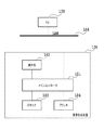
図1は、本実施例に係る半導体集積回路を備える装置の一例としての画像形成装置のシステム構成を示すブロック図である。画像形成装置100は、コピー、プリンタ、FAXといった複数の機能を1台で実現するMFPである。画像形成装置100は、メインコントローラ101、ユーザインタフェースである操作部102、画像入力デバイスであるスキャナ103及び画像出力デバイスであるプリンタ104を備える。
FIG. 1 is a block diagram illustrating a system configuration of an image forming apparatus as an example of an apparatus including a semiconductor integrated circuit according to the present embodiment. The
操作部102、スキャナ103及びプリンタ104は、それぞれメインコントローラ101に接続され、メインコントローラ101からの指示によって制御される。さらに、メインコントローラ101は、LAN(Local Area Network)106に接続され、このLAN106を介してPC105と接続される。
The
PC105は、一般的なコンピュータであり、PC105上で動作するアプリケーションによって作成された文書データ等の印刷指示(印刷ジョブ)がLAN106を介して画像形成装置100に対し送信される。
The PC 105 is a general computer, and a print instruction (print job) such as document data created by an application operating on the PC 105 is transmitted to the
<メインコントローラの構成>
次に、画像形成装置100のメインコントローラ101について詳しく説明する。
<Main controller configuration>
Next, the
図2は、メインコントローラ101の内部構成を示すブロック図である。画像形成装置100の全体を制御するメインコントローラ101は、スキャナ103やプリンタ104を制御する一方で、LAN106を介して、PC105との間で画像データやデバイス情報等の入出力を行う。
FIG. 2 is a block diagram showing an internal configuration of the
メインコントローラ101は、CPU201、メモリコントローラ202、DRAM203、ROM(Read Only Memory)204、クロック生成部205、スキャナ画像処理部206、プリンタ画像処理部207、システムバス208、イメージバス209を備える。さらに、各種インタフェースとして、操作部I/F210、LAN I/F211、イメージバスI/F212、デバイスI/F213、同期・非同期I/F214を備える。
The
CPU(Central Processing Unit)201は、システムバス208を介して、ROM204、イメージバスI/F212、メモリコントローラ202、操作部I/F210、LAN I/F211、同期・非同期I/F214及びクロック生成部205と接続される。ROM204は、システムのブートプログラムや所定の実行プログラムなどが格納される読み出し専用のメモリである。DRAM(Dynamic Random Access Memory)203は、DDR3などのデータ転送速度やデータ転送の仕様が規格化されている半導体メモリであり、CPU201のワークメモリとしての作業領域を提供するための随時読み書き可能な記憶領域である。また、DRAM203は、画像形成装置100の一時的な設定値や実行するジョブの情報などを記憶し、また、画像データを一時記憶するための画像メモリとしても使用される。メモリコントローラ202は、DRAM203を制御するコントローラであり、DRAM203とのデータの読み書きを行う。
A CPU (Central Processing Unit) 201 includes a
操作部I/F210は、操作部102との間で入出力を行うためのインタフェースである。操作部I/F210は、操作部102に対して表示すべき画像データを出力し、また、ユーザが操作部102を介して入力した情報を、CPU201に伝送するために使用される。LAN I/F211は、LAN106と接続するためのインタフェースであり、LAN106に対して情報の入出力を行う。イメージバスI/F212は、システムバス208と画像データを高速で転送するイメージバス209とを接続するインタフェースであり、データ構造を変換するバスブリッジとして動作する。イメージバス209には、デバイスI/F213、スキャナ画像処理部206及びプリンタ画像処理部207が接続される。デバイスI/F2134は、スキャナ103及びプリンタ104とメインコントローラ101とを接続するインタフェースであり、画像データの形式の変換を行う。同期・非同期化I/F214は、システムバス208とメモリコントローラ202間のデータ転送を行うインタフェースである。同期・非同期化I/F214の詳細については後述する。
The operation unit I / F 210 is an interface for performing input / output with the
クロック生成部205は、水晶発振器やPLL(Phase Locked Loop)などの発振回路及び、該発信回路の出力クロックを分周する分周器などを備え、同期回路を動作させる各種クロックを生成して出力する。そして、クロック生成部205は、CPU201、ROM204、メモリコントローラ202、DRAM203、バス208及び209、画像処理部206及び207、各種I/Fなどのメインコントローラ101内の各機能モジュールに各種クロックを供給する。クロック生成部205の構成及び、出力するクロックについての詳細は後述する。なお、メインコントローラ101内の各機能モジュールは、例えばCMOS(Complementary Metal Oxide Semiconductor)の半導体集積回路によって構成される。
The
スキャナ画像処理部206は、スキャナ103から読み込んだ入力画像データに対して、補正、加工、編集等の画像処理を行う。プリンタ画像処理部207は、プリンタ104へ出力する印刷画像データに対して、色変換、フィルタ処理、解像度変換等の画像処理を行う。
A scanner
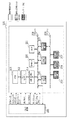
<クロック生成部>
図3は、本実施例に係る、クロック生成部205の内部構成を示すブロック図である。クロック生成部205は、第1クロック源300、第2クロック源310、クロック間引き回路320、クロック設定保持部330を備える。さらに、クロック生成部205は、複数の分周回路とクロックゲート回路(2分周回路360a〜360c、4分周回路361aと361b、8分周回路362、クロックゲート回路370a〜370g)を備える。
<Clock generator>
FIG. 3 is a block diagram illustrating an internal configuration of the
第1クロック源300及び第2クロック源310は、水晶発振器やPLLなどの発振回路であり、それぞれ独自の位相、周波数で発振するクロックを生成して出力する。
The
2分周回路360a〜360c、4分周回路361a及び361b、8分周回路362は、それぞれ自己の前段にあるクロック源や分周回路の出力クロックを入力として、分周クロックを新たに生成する分周回路である。すなわち、2分周回路360a〜360cは周波数が入力クロックの1/2となる分周クロックを生成する。4分周回路361aと361bは周波数が入力クロックの1/4となる分周クロックを生成する。8分周回路362は周波数が入力クロックの1/8となる分周クロックを生成する。なお、本実施例においては分周回路の一例として、2分周、4分周、8分周の分周回路を用いているが、分周数はこれに限定されるものではない。例えば、メインコントローラ101内の機能モジュールが必要とするクロックの周波数に応じて、3分周や16分周の分周回路を備えてもよい。
The divide-by-2
クロックゲート回路370a〜370gは、後述するクロック設定保持部330からのゲート制御信号に基づいて、トグルの有無を制御する。具体的には、ゲート制御信号によってクロックゲート機能をONにしたときに、出力するクロックをLowレベルに固定してクロックの供給(発振)を停止する。図4(a)は、クロックゲート回路によってクロックの発振が停止される様子を説明する図である。図4(a)において、破線の波形で示す部分は、クロックゲート機能をONにしなかった場合(ゲート機能をOFFにした場合)の通常のトグルするクロックを示す。クロック生成部205は、クロックゲート回路370a〜370gを介して、DRAMクロック、メモリコントローラバスクロック、第1インタフェースクロック、CPUクロック、第1バスクロック、第2バスクロック、第2インタフェースクロックをそれぞれメインコントローラ101内の機能モジュールの同期回路に供給する。各クロックと各機能モジュールとの対応関係は以下の通りである。
・DRAMクロック:DRAM203
・メモリコントローラバスクロック:メモリコントローラ202、同期・非同期化I/F214
・第1インタフェースクロック:LAN I/F211
・CPUクロック:CPU201
・第1バスクロック:ROM204、システムバス208、同期・非同期化I/F214
・第2バスクロック:スキャナ画像処理部206、プリンタ画像処理部207、イメージバス209、イメージバスI/F212、デバイスI/F213
・第2インタフェースクロック:操作部I/F210
これらのクロックはそれぞれ個別のクロックゲート回路370a〜370gによってゲート制御することが可能であり、動作不要な機能モジュールの同期回路へのクロックの供給を個別に停止させることによって、画像形成装置100の消費電力を低減することができる。
The clock gate circuits 370a to 370g control the presence / absence of toggle based on a gate control signal from a clock
DRAM clock: DRAM203
Memory controller bus clock:
・ First interface clock: LAN I / F211
CPU clock: CPU201
First bus clock:
Second bus clock: scanner
Second interface clock: operation unit I /
These clocks can be gate-controlled by the individual clock gate circuits 370a to 370g, respectively, and the supply of the clocks to the synchronization circuits of the function modules that do not require operation is individually stopped, thereby consuming the
クロック間引き回路320は、後述するクロック設定保持部330からの間引き制御信号に基づき、内部に備えるクロックゲート回路によって第1クロック源300の出力クロックを基にトグルを間引いたクロック(間引きクロック)を出力する。図4(b)は、クロック間引き回路320によって、第1クロック源300から出力されたクロックが間引かれる様子を説明する図である。間引き制御信号によって、クロック間引きがONになると、連続する4クロックサイクル中の3サイクルを間引いた1サイクル期間を周期的にトグルするクロックが出力されることが示されている。このとき、CPUクロックは、クロック間引き回路320からの出力クロックを2分周回路360bによって2分周したものとなるので、通常時の周波数に対して1/4に低減した周波数(周期は4倍)のクロックとなる。なお、本実施例においてはクロック間引き回路の一例として、4クロックサイクル中の3サイクルを間引いた1サイクル期間を周期的にトグルする例を説明したが、クロックの間引き方はこれに限定されるものではない。例えば、画像形成装置100の消費電力の低減のために必要なクロックの周波数に応じて、7クロックサイクル中の6サイクルを間引くような構成であってもよい。動作を遅くしてもよい機能モジュールの同期回路に対して、このように低減した周波数のクロックを供給することによって、同期回路を動作させたまま画像形成装置100の消費電力を低減することができる。
The
クロック設定保持部330は、クロック間引き回路320及びクロックゲート回路370a〜370gを制御する設定指示の内容を保持し、それぞれのクロック制御信号(間引き制御信号及びゲート制御信号)を出力する回路である。クロック設定保持部330が保持するクロック制御のための設定は、CPU201からシステムバス208を介してなされる。
The clock
<通常クロック出力状態から間引きクロック出力状態への移行>
図5は、クロック間引き回路320が通常のクロックを出力する状態から、間引きクロックを出力する状態に移行する過程を説明する図である。本実施例においては、DRAMクロック、メモリコントローラバスクロック、第1インタフェースクロック、CPUクロック、第1バスクロック及び第2バスクロックは、共通のクロック源である第1クロック源300を基に生成されるクロックである。そのため、これらのクロックは、図5において保線で示す「エッジ一致」のタイミングで立ち上がりエッジが一致する、相互に同期の取れた関係(以下、同期関係)のクロックを構成できる。従って、これらのクロックで動作する同期回路は、データ転送が発生するクロック間でのタイミング設計を行うことによって、同期回路の正常なデータ転送の動作を保障できる。一方、第1クロック源300とは独立したクロック源である第2クロック源310を基に生成される第2インタフェースクロックと上記クロック群とは、同期の取れていない関係(以下、非同期関係)となる。そのため、第2インタフェースクロックで動作する同期回路とのデータ転送にはデータの同期化回路が必要となる。
<Transition from normal clock output state to decimation clock output state>
FIG. 5 is a diagram for explaining a process in which the
また、図4の例では、連続する4クロック中の3クロックを間引く例について説明したので、第1クロック源300を基に生成されるクロックと、当該第1クロック源300からクロック間引き回路320を介して生成されるクロックと、が同期関係となっている。しかし、クロック間引き回路320が、例えば、連続する3クロック中の2クロックを間引く場合、第1クロック源300を基に生成されるクロックと、当該第1クロック源300からクロック間引き回路320を介して生成されるクロックと、が非同期関係となる場合がある。この場合、クロック間引き回路320を介して生成されるクロックが供給される回路とのデータ転送にはデータの同期化回路が必要となる。
In the example of FIG. 4, the example of thinning out three clocks out of four consecutive clocks has been described. Therefore, the clock generated based on the
なお、クロック生成部205が出力するクロックの中でDRAMクロック、メモリコントローラバスクロック、第1インタフェースクロックは、クロック間引き回路320から出力されるクロックとは無関係の、周波数が固定のクロックである。これらは、周波数が動的に変化することが許可されない場合や、周波数が予め定められた所定の周波数でなければならない場合に使用されるクロックである。そして、CPUクロック、第1バスクロック、第2バスクロックは、クロック間引き回路320が出力するクロックを基に分周して生成される分周クロックであり、クロックの間引き設定にしたがって、周波数が可変のクロックである。図5に示す「クロック間引きON」のタイミングでクロック間引き設定がONになると、クロック間引き回路320が出力するクロックの周波数が低減する。このように、クロック間引き回路320が通常時の周波数から低減した周波数を出力するように変わる際、クロックの周波数比が変わるだけでなく、どのくらい間引くかによって位相もずれてしまう。図5の例では、メモリコントローラバスクロックと第1バスクロックは、周波数比1:1の関係から4:1の関係に変わるのみで、立ち上がりエッジが一致するタイミングが4サイクルに1回は存在している。
Of the clocks output from the
<間引きクロック出力状態から通常クロック出力状態への移行>
図6は、クロック間引き回路320が間引きクロックを出力する状態から、通常のクロックを出力する状態に移行する過程を説明する図である。図6に示す「クロック間引きOFFのタイミングでクロック間引き設定がOFFになると、クロック間引き回路320が出力するクロックは通常時の周波数に戻る。このように、クロック間引き回路320から出力されるクロックの周波数が、低減した状態から通常の状態に戻る際に、上述したクロックの周波数比も元に戻る。例えば、上述のメモリコントローラバスクロックと第1バスクロックとの間の周波数比は、4:1の関係から1:1の関係に戻り、立ち上がりエッジのタイミングは毎サイクル一致することになる。
<Transition from the thinned clock output state to the normal clock output state>
FIG. 6 is a diagram for explaining a process in which the
<画像形成装置における省電力制御>
次に、画像形成装置100のメインコントローラ101による省電力制御について説明する。画像処理装置100は、その稼動状態に応じて消費電力の異なる2種類の動作モード(通常モードと省電力モード)を備える。画像形成装置100は、操作部102が所定の期間中にユーザからの操作を受け付けなかった場合や、印刷ジョブを実行しなかった場合に、通常の動作状態である通常モードから、消費電力を低減した待機状態である省電力モードに移行する。従って、省電力モードにおいては印刷ジョブなどを実行することはなく、メインコントローラ101上の一部の機能モジュールは動作する必要のない状態、あるいは、動作速度を低減しても支障がない状態になる。すなわち、省電力モード下では、クロック生成部205がメインコントローラ101上の一部の機能モジュールに供給するクロックを停止、あるいは、周波数を低減することができる状態となっている。
<Power Saving Control in Image Forming Apparatus>
Next, power saving control by the
図7は、省電力モード時における、メインコントローラ101の各機能モジュールへのクロックの供給状態を示す図である。図7において、クロック生成部205から出力される通常クロック(すなわち、低減されていない周波数のクロック)で動作するモジュールは、DRAM203、メモリコントローラ202、操作部I/F210、LAN I/F211、同期・非同期化I/F214である。そして、クロック生成部205から出力される間引きクロック(すなわち、低減された周波数のクロック)で動作するモジュールは、CPU201、ROM204及びシステムバス208である。さらに、クロックゲート回路のゲート制御によりクロック生成部205からのクロック供給が停止することで、動作を停止するモジュールは、イメージバスI/F212、デバイスI/F213、スキャナ画像処理部206、プリンタ画像処理部207、イメージバス209である。
FIG. 7 is a diagram showing a clock supply state to each functional module of the
省電力モード時には、このようにクロック周波数の低減、或いは、クロック供給の停止によって、消費電力を通常モードよりも低く抑えることができる。そして、操作部102を介した復帰指示操作をユーザが行ったり、PC105からLAN106を介して印刷ジョブを受信すると、停止しているクロック供給が再開され、或いは低減されていたクロックの周波数が通常の周波数に戻される。これにより、画像形成装置100は、省電力モードから通常モードへと復帰し、印刷ジョブなどの処理の実行が可能な状態となる。
In the power saving mode, the power consumption can be kept lower than that in the normal mode by reducing the clock frequency or stopping the clock supply. When the user performs a return instruction operation via the
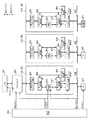
<同期・非同期化I/F>
続いて、同期・非同期化I/F214の詳細について説明する。図8は、同期・非同期化I/F214の内部構成とその動作を説明する図である。
<Synchronization / asynchronization I / F>
Next, details of the synchronization / asynchronization I /
図8(a)には、クロック生成部205から出力されるクロックのうち、DRAMクロック、メモリコントローラバスクロック、第1バスクロック、CPUクロックの供給先が示されている。DRAMクロックは、メモリコントローラ202を介してDRAM203に供給される。メモリコントローラバスクロックは、メモリコントローラ202と同期・非同期化I/F214に供給される。第1バスクロックは、システムバス208と同期・非同期化I/F214に供給される。そして、CPUクロックは、CPU201に供給される。
FIG. 8A shows the supply destination of the DRAM clock, the memory controller bus clock, the first bus clock, and the CPU clock among the clocks output from the
メモリコントローラ202内では、DRAMクロックとメモリコントローラバスクロックは、周波数比が2:1の固定された同期関係でデータのやり取りを行う。また、メモリコントローラ202を介して、DRAM203とのデータ転送に使用されるDRAMクロックは、DRAM203の動作中に動的に周波数が変化することは好ましくない。そのため、DRAMクロック及び該DRAMクロックと同期関係にあるメモリコントローラバスクロックは、周波数が固定である。
In the
CPUクロックと第1バスクロックは、クロック間引き回路320における間引き制御によって、前述の図5で示したように周波数が低減される。CPUクロックと第1バスクロックは、周波数比(すなわち、同期関係)を維持したまま周波数が低減されるため、CPU201及びシステムバス208上のデータ転送は問題なく行うことができる。
The frequency of the CPU clock and the first bus clock is reduced by the thinning control in the
続いて、同期・非同期化I/F214の内部構成について説明する。同期・非同期化I/F214は、バスインタフェース回路801、第1データパス選択回路802、同期化回路803、第2データバス選択回路804、メモリコントローラインタフェース回路805、データパス設定保持回路806から構成される。
Next, the internal configuration of the synchronization / asynchronization I /
バスインタフェース回路801は、システムバス208側のバスプロトコルに則った同期のデータ転送を行う。
The
メモリコントローラインタフェース回路805は、メモリコントローラ202側のインタフェース仕様に基づいた同期のデータ転送を行う。
The memory
第1データパス選択回路802は、使用するデータパス(すなわち、同期化回路803と第2データパス選択回路804とのどちらとデータのやり取りを行うか)を、データパス選択制御信号に基づいて選択するセレクタ回路である。
The first data
第2データパス選択回路804は、使用するデータパス(すなわち、第1データパス選択回路802と同期化回路803とのどちらとデータのやり取りを行うか)をデータパス選択制御信号に基づいて選択するセレクタ回路である。
The second data
データパス設定保持回路806は、CPU201から送られてくるデータパス選択の設定指示を保持し、保持したデータパス選択設定を第1データパス選択回路802と第2データパス選択回路804に対し、データパス選択制御信号として出力する。
The data path setting holding
同期化回路803は、バスインタフェース回路801に供給されるクロック同期のデータとメモリコントローラインタフェース回路805に供給されるクロック同期のデータを、それぞれ受信する側のクロック同期のデータに変換する回路である。この同期化回路803は、例えばFIFO(First In First Out)のバッファで構成され、バスインタフェース回路801から入力したデータをメモリコントローラインタフェース回路805に出力し、メモリコントローラインタフェース回路805から入力したデータをバスインタフェース回路801に出力する。
The
同期・非同期化I/F214に供給されたメモリコントローラバスクロックは、メモリコントローラインタフェース回路805と同期化回路803に供給される。また、同期・非同期化I/F214に供給された第1バスクロックは、バスインタフェース回路801と同期化回路803に供給される。
The memory controller bus clock supplied to the synchronization / asynchronization I /
ここで、メモリコントローラバスクロックは周波数が固定であるのに対し、第1バスクロックは周波数が可変であるため、省電力モードにおいてはメモリコントローラバスクロックと第1バスクロックとは同期関係でなくなるときがある。図8(b)は、第1バスクロックの周波数が通常時の周波数であって、メモリコントローラバスクロックと第1バスクロックとが同期関係にあるときの同期・非同期化I/F214内のデータパスの使用を示す図である。図8(b)において、第1データパス選択回路802と第2データパス選択回路804は、データ選択制御信号に従い、バスインタフェース回路801とメモリコントローラインタフェース回路805との間で直接にデータ転送を行う同期データパスを選択する。このとき、メモリコントローラインタフェース回路805に供給されるメモリコントローラバスクロックとバスインタフェース回路801に供給される第1バスクロックは、同じ位相かつ同じ周波数のクロックである。従って、システムバス208とメモリコントローラ202の間は、クロック同期で遅延のない高速なデータ転送を行うことができる。
Here, the frequency of the memory controller bus clock is fixed, whereas the frequency of the first bus clock is variable, so that the memory controller bus clock and the first bus clock are not synchronized in the power saving mode. There is. FIG. 8B shows a data path in the synchronization / asynchronization I /
一方、図8(c)は、第1バスクロックの周波数が通常時よりも低減した周波数であって、メモリコントローラバスクロックと第1バスクロックとが同期関係にないときときの同期・非同期化I/F214内のデータパスの使用を示す図である。図8(c)において、第1データパス選択回路802と第2データパス選択回路804は、データ選択制御信号に従い、バスインタフェース回路801とメモリコントローラインタフェース回路805との間のデータ転送を、同期化回路803を介して行なう非同期データパスを選択する。このとき、メモリコントローラインタフェース回路805に供給されるメモリコントローラバスクロックとバスインタフェース回路801に供給される第1バスクロックとは、周波数のみならず位相も異なっている可能性がある。従って、同期化回路803を介することによって、入力側のインタフェース回路のクロックから出力側のインタフェース回路のクロックへの乗せ換えに要するデータ転送の遅延は生じるが、安全な(システムバス807とメモリコントローラ202との間でデータの消失など発生することのない)データ転送を行うことができる。なお、図4に示したように、同一のクロック源の4サイクルのうち3サイクルを間引いた間引きクロックから可変分周クロックを生成する本実施例の場合は、低減させた周波数においても立ち上がりエッジが一致するタイミングが存在することになる。この場合、理論的には同期化回路を経由する必要はないということになるが、省電力モードでは高速なデータ転送は要求されないので、同期化回路を介したデータパスを選択しても支障はない。
On the other hand, FIG. 8C shows the synchronization / asynchronization I when the frequency of the first bus clock is lower than normal and the memory controller bus clock and the first bus clock are not in a synchronous relationship. It is a figure which shows use of the data path in / F214. In FIG. 8C, the first data
<データパス制御・クロック制御>
次に、本実施例に係る、メインコントローラ101によるデータパス制御とクロック制御について、フローチャートを参照して説明する。
<Data path control / clock control>
Next, data path control and clock control by the
まず、通常モードから省電力モードに移行する際の制御について、図9を参照して説明する。 First, control when shifting from the normal mode to the power saving mode will be described with reference to FIG.
ステップ901において、メインコントローラ101内のCPU201は、通常モードから省電力モードに移行する原因が生じたかどうかを判定する。この原因には、例えば印刷ジョブの実行がないまま所定時間(例えば、15分)が経過したこと等が挙げられる。このような所定の原因の発生が確認された場合は、ステップ902に進む。一方、このような所定の原因の発生が確認されない場合は、その監視を継続する。
In
ステップ902において、CPU201は、非同期データパスを選択するデータパス選択設定の指示を、システムバス208を介して同期・非同期化I/F214に送信する。
In
ステップ903において、同期・非同期化I/F214は、受信したデータパス選択設定指示の内容を保持すると共に、第1データパス選択回路802と第2データパス選択回路804に対し非同期データパスを選択する設定を行なう。これにより、バスインタフェース回路801とメモリインタフェース回路805との間のデータパスとして、同期化回路803を介したデータパスが選択される。データパスの設定が完了すると、同期・非同期化I/F214は、例えば割り込み信号を用いて、CPU201にデータパスの設定完了を通知する。
In step 903, the synchronization / asynchronization I /
ステップ904において、CPU201は、特定のクロックのゲートをONにする設定指示とクロックを間引く設定指示を、システムバス208を介してクロック生成部205に送信する。
In step 904, the
ステップ905において、クロック生成部205内のクロック設定保持部330は、受信した2種類の設定指示の内容を保持すると共に、所定の制御信号を出力する。すなわち、対応するクロックゲート回路にゲートをONにするゲート制御信号を出力し、クロック間引き回路320に間引きをONにする間引き制御信号を出力する。この場合において、前述の図7の状態を実現するための制御信号の詳細は以下の通りである。
In step 905, the clock

ステップ906において、クロック生成部205内の特定のクロックゲート回路(上述の例ではクロックゲート回路370f)は、クロック設定保持部330からのゲート制御信号に基づいてゲートをONにする。これにより、動作を停止しても構わない所定の機能モジュールへのクロックの供給が停止される。
In
ステップ907において、クロック生成部205内のクロック間引き回路320は、クロック設定保持部330からの間引き制御信号に基づいて間引きをONにする。これにより、動作速度を遅くしても構わない所定の機能モジュールに対し低減された周波数のクロックが供給される。こうして、省電力モードへの移行処理が完了する。
In
以上が、通常モードから省電力モードに移行する際の制御処理の内容である。なお、図9から明らかなように、ステップ906とステップ907は並列に処理される。これにより、画像形成装置100の消費電力を低く抑えながら、システムバス208とメモリコントローラ202との間でデータの消失などが発生することのない安全なデータ転送が可能となる。
The above is the content of the control processing when shifting from the normal mode to the power saving mode. As is apparent from FIG. 9,
次に、省電力モードから通常モードに復帰する際の制御について、図10を参照して説明する。 Next, control when returning from the power saving mode to the normal mode will be described with reference to FIG.
ステップ1001において、メインコントローラ101内のCPU201は、省電力モードから通常モードに移行する原因が生じたかどうかを判定する。この原因には、例えばPC105からLAN106を介して印刷ジョブを受信したこと等が挙げられる。このような所定の原因の発生が確認された場合は、ステップ1002に進む。一方、このような所定の原因の発生が確認されない場合は、その監視を継続する。
In step 1001, the
ステップ1002において、CPU201は、停止されていた特定のクロックの供給を再開する設定指示と低減されていた特定のクロックの周波数を通常の周波数に戻す設定指示を、システムバス208を介してクロック生成部205に送信する。
In step 1002, the
ステップ1003において、クロック生成部205内のクロック設定保持部330は、受信した2種類の設定指示の内容を保持すると共に、所定の制御信号を出力する。具体的には、対応するクロックゲート回路(上述の例では、クロックゲート回路370f)に対し、ゲートをOFFにするゲート制御信号を出力する。さらに、クロック間引き回路320に対し、間引きをOFFにする間引き制御信号を出力する。
In step 1003, the clock
ステップ1004において、クロック生成部205内の特定のクロックゲート回路(上述の例では、クロックゲート回路370f)は、クロック設定保持部330からのゲート制御信号に基づいてゲートをOFFにする。これにより、クロックの供給が再開される。
In
ステップ1005において、クロック生成部205内のクロック間引き回路320は、クロック設定保持部330からの間引き制御信号に基づいて間引きをOFFにする。これにより、通常の周波数のクロックの出力が再開される。
In
ステップ1006において、CPU201は、同期データパスを選択するデータパス選択設定の指示を、システムバス208を介して同期・非同期化I/F214に送信する。
In
ステップ1007において、同期・非同期化I/F214は、受信したデータパス選択設定指示の内容を保持すると共に、第1データパス選択回路802と第2データパス選択回路804に対して上述の同期データパスを選択する設定を行なう。これにより、バスインタフェース回路801とメモリコントローラインタフェース回路805との間のデータパスとして、同期化回路803を介さない(回路801と回路805との間で直接データ転送を行う)データパスが設定される。データパスの設定が完了すると、同期・非同期化I/F214は、例えば割り込み信号を用いて、CPU201にデータパスの設定完了を通知する。こうして、通常モードへの復帰処理が完了する。
In step 1007, the synchronization / asynchronization I /
以上が、省電力モードから通常モードに移行する際の制御処理の内容である。なお、図10から明らかなように、ステップ1004とステップ1005は並列に処理される。これにより、通常モードへの復帰後に、システムバス208とメモリコントローラ202との間で遅延のないクロック同期のデータ転送が可能となる。
The above is the content of the control processing when shifting from the power saving mode to the normal mode. As is clear from FIG. 10,
なお、上述の図9及び図10のフローチャートにおけるデータパスの選択・設定は、システムバス208とDRAM203との間でデータ転送が行なわれていない状態で行う必要がある。そのため、DRAM203がCPU201のワークメモリとして使用されている場合などは、上記フローの制御は、例えばCPU201がROM204に格納されたプログラムを処理することで実現される。
Note that the selection and setting of the data path in the flowcharts of FIGS. 9 and 10 described above must be performed in a state where no data transfer is performed between the
また、本実施例では、同期・非同期化I/F214を独立した機能モジュールとして説明したが、メモリコントローラ202内に、同期・非同期化I/F214に相当する機能を有する構成でもよい。
In this embodiment, the synchronization / asynchronization I /
さらに、本実施例では、可変周波数のクロックで動作するシステムバス208と固定周波数のクロックで動作するメモリコントローラ202との間のデータ転送を円滑に行なうべく両者の間に同期・非同期化I/F214を設ける構成としたが、この構成に限られない。可変周波数のクロックで動作する機能モジュールと固定周波数のクロックで動作する機能モジュールとの間で、同期と非同期のデータ転送が発生し得る状況下において、両機能モジュールの間に上述の同期・非同期化I/Fを設けることで同様の効果が得られる。
Further, in this embodiment, in order to smoothly transfer data between the
以上の通り本実施例によれば、複数の異なる種類のクロックが同期関係にない場合において、クロックのエッジ位置が相互に一致しない構成の下でもデータ転送が可能である。また、これらクロックが同期関係にある場合には遅延のないデータ転送を行うことができ、たとえ非同期関係にある場合でも安全なデータ転送を行うことができる。 As described above, according to this embodiment, when a plurality of different types of clocks are not in a synchronous relationship, data transfer is possible even under a configuration in which the clock edge positions do not match each other. Further, when these clocks are in a synchronous relationship, data transfer without delay can be performed, and even when they are in an asynchronous relationship, safe data transfer can be performed.
実施例1は、周波数が固定のクロックと周波数が可変のクロックとの間のデータ転送において、同期用のデータパスと非同期用のデータパスを選択的に切り替える態様であった。そして、周波数が固定のクロックと周波数が可変のクロックのいずれも、共通の第1クロック源300から分周して生成されていた。そのため、異なる周波数のクロックであっても立ち上がりエッジが一致するタイミングが必ず存在し、クロック生成部205におけるクロックの生成の仕方を工夫することで、機能モジュール間のデータ転送を同期で扱うことができた。
In the first embodiment, in the data transfer between the clock having a fixed frequency and the clock having a variable frequency, the synchronous data path and the asynchronous data path are selectively switched. Both the fixed frequency clock and the variable frequency clock are generated by frequency division from the common
しかしながら、省電力モード時に使用するための低減された周波数を、異なるクロック源(より低周波数のクロック源)を用いて生成する場合もある。この場合は、省電力モード時に用いるための同期関係にある周波数が低減されたクロックの生成が困難である。 However, the reduced frequency for use during the power saving mode may be generated using a different clock source (a lower frequency clock source). In this case, it is difficult to generate a clock with a reduced frequency in a synchronous relationship for use in the power saving mode.
そこで、省電力モード時の低減された周波数を異なるクロック源を用いて生成する場合における、機能モジュール間のデータ転送を円滑に行なうための態様を、実施例2として説明する。なお、実施例1と共通する部分(画像形成装置100の基本構成及びメインコントローラ101の内部構成)については説明を省略し、以下では、差異点(クロック生成部の内部構成と動作モードの移行制御)を中心に説明するものとする。
Thus, an embodiment for smoothly transferring data between functional modules when a reduced frequency in the power saving mode is generated using different clock sources will be described as a second embodiment. The description of the parts common to the first embodiment (the basic configuration of the
<クロック生成部>
図11は、本実施例に係る、クロック生成部205’の内部構成を示すブロック図である。本実施例のクロック生成部205’は、第1クロック源300、第2クロック源310に加えて、第3クロック源1100を備える。また、クロック間引き回路320に代えてクロック選択回路1110を備え、該クロック選択回路1110の設定を行なうクロック設定保持部1120を備える。さらに、クロック生成部205’は、複数の分周回路とクロックゲート回路(2分周回路360a、360c、360d、4分周回路361aと361b、8分周回路362、クロックゲート回路370a〜370g)を備える。
<Clock generator>
FIG. 11 is a block diagram illustrating an internal configuration of the
第3クロック源1100は、他のクロック源と同様に、水晶発振器やPLLなどで構成される発振回路であり、第1クロック源300の2分周クロックの周波数よりも低い周波数で発振する。例えば、第1クロック源300の周波数は1600MHz、第2クロック源310の周波数は20MHz、第3クロック源1100の周波数は50MHzといった具合である。上述の通り、第3クロック源1100は、省電力モード時の消費電力を低く抑える際に用いるクロックである。
The
クロック選択回路1110は、後述するクロック設定保持部1120からのクロック選択制御信号に基づいて、第1クロック源300を基に2分周する2分周回路360dの出力クロックと第3クロック源1100の出力クロックのどちらかを選択して出力する。省電力モード時には、動作を遅くしても構わない機能モジュールに対し周波数の低い第3クロック源のクロックを供給することによって、機能モジュールの同期回路を動作させたまま画像形成装置100の消費電力を低減することができる。
Based on a clock selection control signal from a clock
クロック設定保持部1120は、クロック選択回路1110及びクロックゲート回路370a〜370gを制御する設定指示の内容を保持し、それぞれのクロック制御信号(選択制御信号及びゲート制御信号)を出力する回路である。クロック設定保持部1120が保持するクロック制御のための設定は、CPU201からシステムバス208を介してなされる。
The clock
<クロック選択回路によるクロックの切り替え>
まず、第1クロック源300を2分周した分周クロックを選択した状態から、第3クロック源1100の出力クロックを選択した状態へと切り替える場合について説明する。
<Clock switching by clock selection circuit>
First, a case where the state is switched from the state where the divided clock obtained by dividing the
図12は、クロック選択回路1110が、第1クロック源300を基に2分周する2分周回路360dの出力クロックを選択した状態から、第3クロック源1100の出力クロックを選択する状態に移行する過程を説明する図である。図12において破線で示す「選択切替」のタイミングで、第1クロック源300を2分周した分周クロックを選択した状態から、第3クロック源1100の出力クロックを選択した状態へと切り替わることで、クロック選択回路1110の出力クロックの周波数は低減する。
12 shifts from the state where the clock selection circuit 1110 selects the output clock of the divide-by-2 circuit 360d that divides the frequency by 2 based on the
図12において、「選択切替」のタイミングの前では、クロック選択回路1110が選択しているクロックは、第1クロック源300を基に2分周した分周クロックである。このとき、DRAMクロック、メモリコントローラバスクロック、第1インタフェースクロック、CPUクロック、第1バスクロック、第2バスクロックは、共通の第1クロック源300を基に生成されたクロックである。そのため、これらのクロックは、図12における「選択切替」のタイミングで立ち上がりエッジが一致するクロック、すなわち同期関係にあるクロックとなる。従って、これらのクロックで動作する同期回路は、データ転送が行なわれるクロック間でのタイミング設計を行うことによって、その動作を保障できる。
In FIG. 12, before the “selection switching” timing, the clock selected by the clock selection circuit 1110 is a divided clock divided by two based on the
一方、図12において、「選択切替」のタイミングの後では、クロック選択回路1110が選択しているクロックは、第3クロック源1100の出力クロックである。このとき、第1クロック源を基に生成される上述のクロック群と、第3クロック源を基に生成されるクロック群(CPUクロック、第1バスクロック、第2バスクロック)とは、位相及び周波数が異なり、互いに非同期関係にある。従って、これらの非同期関係にあるクロック間で動作する回路においては、データ転送の遅延が生じたとしても、データの消失などが発生することなく安全にデータを転送するための同期化回路が必要となる。
On the other hand, in FIG. 12, after the “selection switching” timing, the clock selected by the clock selection circuit 1110 is the output clock of the
次に、第3クロック源1100の出力クロックを選択した状態から、第1クロック源300を2分周した分周クロックを選択した状態へと切り替える場合について説明する。
Next, a case where the output clock of the
図13は、クロック選択回路1110が第3クロック源1100の出力クロックを選択した状態から、第1クロック源300を基に2分周した分周クロックを選択する状態に移行する過程を説明する図である。図13において破線で示す「選択切替」のタイミングで、第3クロック源1100の出力クロックを選択した状態から、第1クロック源300を2分周した分周クロックを選択した状態に切り替わることで、クロック選択回路1110の出力クロックの周波数は通常時の周波数に戻る。さらに、固定周波数のクロックであるDRAMクロック等のクロック群と可変周波数のクロックであるCPUクロック等のクロック群とが、図13における「エッジ一致」のタイミングで立ち上がりエッジが一致するようになる。これにより、第2インタフェースクロックを除くすべてのクロックの同期が取れた状態に戻る。
FIG. 13 is a diagram for explaining a process in which the clock selection circuit 1110 shifts from the state in which the output clock of the
<データパス制御・クロック制御>
続いて、本実施例に係る、メインコントローラ101によるデータパス制御とクロック制御について、フローチャートを参照して説明する。
<Data path control / clock control>
Next, data path control and clock control by the
まず、通常モードから省電力モードに移行する際の制御について、図14を参照して説明する。 First, control when shifting from the normal mode to the power saving mode will be described with reference to FIG.
ステップ1401〜ステップ1403は、実施例1の図9のフローにおけるステップ901〜ステップ903に対応する。すなわち、省電力モードに移行する原因が生じたかどうかの判定(S1401)、非同期データパスを選択する設定指示の同期・非同期化I/F214への送信(S1402)、非同期データパスの選択設定(S1403)が実行される。
ステップ1404において、CPU201は、特定のクロックのゲートをONにする設定指示と第3クロック源1100の出力クロック選択の設定指示を、システムバス208を介してクロック生成部205’に送信する。
In step 1404, the
ステップ1405において、クロック生成部205’内のクロック設定保持部1120は、受信した2種類の設定指示の内容を保持すると共に、所定の制御信号を出力する。すなわち、対応するクロックゲート回路に対しゲートをONにするゲート制御信号を出力し、クロック選択回路1110に対し第3クロック源1100の出力クロックの選択を指示する制御信号を出力する。
In step 1405, the clock
ステップ1406は、実施例1の図9のフローにおけるステップ906に対応する。すなわち、クロック生成部205’内の対応するクロックゲート回路は、クロック設定保持部1120からのゲート制御信号に基づいてゲートをONにする。これにより、動作を停止しても構わない所定の機能モジュールへのクロックの供給が停止される。
Step 1406 corresponds to step 906 in the flow of FIG. 9 of the first embodiment. That is, the corresponding clock gate circuit in the
ステップ1407において、クロック生成部205’内のクロック選択回路1110は、クロック設定保持部1120からの選択制御信号に基づいて、選択するクロックを切り替える。具体的には、第1クロック源300を2分周した分周クロックを選択した状態から、第3クロック源1100の出力クロックを選択した状態へと切り替える。これにより、動作速度を遅くしても構わない所定の機能モジュールに対し低減された周波数のクロックが供給される。こうして、省電力モードへの移行処理が完了する。
In step 1407, the clock selection circuit 1110 in the
以上が、本実施例に係る、通常モードから省電力モードに移行する際の制御処理の内容である。これにより、システムバス208とメモリコントローラ202との間でデータの消失などが発生することのない安全なデータ転送が可能となる。
The above is the content of the control processing when shifting from the normal mode to the power saving mode according to the present embodiment. This enables safe data transfer between the
次に、省電力モードから通常モードに復帰する際の制御処理について、図15を参照して説明する。 Next, a control process when returning from the power saving mode to the normal mode will be described with reference to FIG.
ステップ1501は、実施例1の図10のフローにおけるステップ1001に対応する。すなわち、通常モードに移行する原因が生じたかどうかの判定(S1501)が実行される。 Step 1501 corresponds to step 1001 in the flow of FIG. That is, it is determined whether or not a cause for shifting to the normal mode has occurred (S1501).
ステップ1502において、CPU201は、停止されていた特定のクロックのゲートをOFFにする設定指示と第1クロック源300に基づく2分周クロック(通常時の周波数のクロック)選択の設定指示を、システムバス208を介してクロック生成部205’に送信する。
In
ステップ1503において、クロック生成部205’内のクロック設定保持部1120は、受信した2種類の設定指示の内容を保持すると共に、所定の制御信号を出力する。具体的には、対応するクロックゲート回路に対しゲートをOFFにするゲート制御信号を出力し、クロック選択回路1110に対し第1クロック源300を基に生成された2分周クロックの選択を指示する制御信号を出力する。
In
ステップ1504は、実施例1の図10のフローにおけるステップ1004に対応する。すなわち、クロック生成部205’内の特定のクロックゲート回路は、クロック設定保持部1120からのゲート制御信号に基づいてゲートをOFFにする。これにより、クロックの供給が再開される。
ステップ1505において、クロック生成部205’内のクロック選択回路1110は、クロック設定保持部1120からの選択制御信号に基づいて、選択するクロックを切り替える。具体的には、第3クロック源1100の出力クロックを選択した状態から、第1クロック源300を2分周した分周クロックを選択した状態へと切り替える。これにより、通常時の周波数のクロックが出力される。
In
ステップ1506及びステップ1507は、実施例1の図10のフローにおけるステップ1006及びステップ1007に対応する。すなわち、同期データパスを選択する選択設定指示の送信(S1506)、及び同期データパスを選択する設定(S1507)が実行される。こうして、通常モードへの復帰処理が完了する。
以上が、本実施例に係る、省電力モードから通常モードに復帰する際の制御処理の内容である。これにより、システムバス208とメモリコントローラ202との間で遅延のないクロック同期のデータ転送を行えるようになる。
Step 1506 and
The above is the content of the control processing when returning from the power saving mode to the normal mode according to the present embodiment. As a result, clock-synchronized data transfer without delay can be performed between the
以上のとおり本実施例によれば、通常モード時は、単一のクロック源を用いた同期関係にある複数のクロックによって遅延のない同期データ転送を行うことができる。また、省電力モード時は、より低周波数の独立したクロック源を用いて消費電力を低減しながら、非同期関係にあるクロックによって安全なデータ転送を行うことができる。 As described above, according to the present embodiment, in the normal mode, synchronous data transfer without delay can be performed by a plurality of clocks having a synchronous relationship using a single clock source. Also, in the power saving mode, safe data transfer can be performed using asynchronous clocks while reducing power consumption using a lower frequency independent clock source.
[その他の実施形態]
本発明は、以下の処理を実行することによっても実現される。すなわち、上述した実施形態の機能を実現するソフトウェア(プログラム)を、ネットワーク又は各種記憶媒体を介してシステムあるいは装置に供給し、そのシステムあるいは装置のコンピュータ(又はCPUやMPU等)がプログラムを読み出して実行する処理である。
[Other Embodiments]
The present invention is also realized by executing the following processing. That is, software (program) that realizes the functions of the above-described embodiments is supplied to a system or apparatus via a network or various storage media, and a computer (or CPU, MPU, etc.) of the system or apparatus reads the program. It is a process to be executed.
Claims (18)
前記クロック源が出力した前記クロック信号を第1周波数又は前記第1周波数より小さい第2周波数で出力する周波数可変回路と、
前記周波数可変回路から出力されたクロック信号が入力される第1デバイスと、
前記周波数可変回路を介さずに前記クロック源から出力されたクロック信号が入力される第2デバイスと、前記第1デバイスと前記第2デバイスとの間のデータ転送を行うインターフェースと、を備え、
前記インターフェースは、
同期化回路を有し、
前記周波数可変回路が前記第2周波数のクロック信号を出力する場合には、前記同期化回路を介してデータ転送を行い、
前記周波数可変回路が前記第1周波数のクロック信号を出力する場合には、前記同期化回路を介さずにデータ転送を行う、
ことを特徴とする半導体集積回路。 A clock source for outputting a clock signal;
A frequency variable circuit that outputs the clock signal output from the clock source at a first frequency or a second frequency smaller than the first frequency;
A first device to which a clock signal output from the frequency variable circuit is input;
A second device to which a clock signal output from the clock source is input without going through the frequency variable circuit, and an interface for transferring data between the first device and the second device,
The interface is
Having a synchronization circuit,
When the frequency variable circuit outputs the clock signal of the second frequency, data transfer is performed via the synchronization circuit,
When the frequency variable circuit outputs the clock signal of the first frequency, data transfer is performed without going through the synchronization circuit.
A semiconductor integrated circuit.
所定の指示に従って、前記クロック源から入力された前記クロック信号を前記第2周波数で出力し、
他の所定の指示に従って、前記クロック源から入力された前記クロック信号を前記第1周波数で出力する、
ことを特徴とする請求項1又は2に記載の半導体集積回路。 The frequency variable circuit is:
According to a predetermined instruction, the clock signal input from the clock source is output at the second frequency,
According to another predetermined instruction, the clock signal input from the clock source is output at the first frequency.
The semiconductor integrated circuit according to claim 1 or 2, wherein
前記周波数可変回路から出力されたクロック信号の周波数を分周する第2分周回路と、をさらに備え、
前記第1分周回路から出力されたクロック信号は、前記第2デバイスに入力され、
前記第2分周回路から出力されたクロック信号は、前記第1デバイスに入力される、
ことを特徴とする請求項1乃至5の何れか1項に記載の半導体集積回路。 A first frequency divider for dividing the frequency of the clock signal output from the clock source;
A second frequency divider that divides the frequency of the clock signal output from the frequency variable circuit;
The clock signal output from the first frequency divider is input to the second device,
The clock signal output from the second frequency divider circuit is input to the first device.
The semiconductor integrated circuit according to claim 1, wherein the semiconductor integrated circuit is a semiconductor integrated circuit.
通常モードと該通常モードよりも消費電力が低い省電力モードとで動作可能であり、
前記通常モードから前記省電力モードに移行する際に、前記所定の指示が出力され、前記省電力モードから前記通常モードに移行する際に、前記他の所定の指示が出力される、
ことを特徴とする装置。 A semiconductor integrated circuit according to claim 3,
It is possible to operate in the normal mode and the power saving mode in which the power consumption is lower than the normal mode,
The predetermined instruction is output when shifting from the normal mode to the power saving mode, and the other predetermined instruction is output when shifting from the power saving mode to the normal mode.
A device characterized by that.
周波数可変回路によって、クロック源が出力したクロック信号を第1周波数又は前記第1周波数より小さい第2周波数で出力するステップと、
同期化回路を有するインターフェースによって、前記周波数可変回路から出力されたクロック信号が入力される第1デバイスと、前記周波数可変回路を介さずに前記クロック源から出力されたクロック信号が入力される第2デバイスとの間のデータ転送を行うステップであって、
前記周波数可変回路から前記第2周波数のクロック信号が出力された場合には、前記同期化回路を介してデータ転送を行い、
前記周波数可変回路から前記第1周波数のクロック信号が出力された場合には、前記同期化回路を介さずにデータ転送を行う、ステップと、
を含むことを特徴とするクロックの制御方法。 A method for controlling a clock in a semiconductor integrated circuit, comprising:
Outputting a clock signal output from a clock source at a first frequency or a second frequency smaller than the first frequency by a frequency variable circuit;
A first device to which a clock signal output from the frequency variable circuit is input by an interface having a synchronization circuit, and a second device to which a clock signal output from the clock source is input without passing through the frequency variable circuit. A step of transferring data to and from the device,
When the clock signal having the second frequency is output from the frequency variable circuit, the data is transferred through the synchronization circuit,
When the clock signal having the first frequency is output from the frequency variable circuit, data is transferred without passing through the synchronization circuit; and
A method for controlling a clock, comprising:
前記クロック源から入力された前記クロック信号を第1周波数又は前記第1周波数より小さい第2周波数で出力する周波数可変回路と、
前記クロック源から出力された、前記周波数可変回路を介さない前記クロック信号の周波数を分周する第1の分周回路と、
前記周波数可変回路から出力されたクロック信号の周波数を分周する第2の分周回路と、
前記第2の分周回路から出力されたクロック信号が入力される第1デバイスと、
前記第1の分周回路から出力されたクロック信号が入力される第2デバイスと、
前記第1デバイスと前記第2デバイスとの間のデータ転送を行うインターフェースと、を備え、
前記インターフェースは、
同期化回路を有し、
前記周波数可変回路が出力するクロック信号の周波数に応じて、前記同期化回路を介したデータ転送、又は、前記同期化回路を介さないデータ転送を行う、
ことを特徴とする半導体集積回路。 A clock source for outputting a clock signal;
A frequency variable circuit that outputs the clock signal input from the clock source at a first frequency or a second frequency smaller than the first frequency;
A first frequency divider that divides the frequency of the clock signal that is output from the clock source and not via the frequency variable circuit;
A second frequency divider that divides the frequency of the clock signal output from the frequency variable circuit;
A first device to which the clock signal output from the second frequency divider circuit is input ;
A second device to which the clock signal output from the first frequency divider circuit is input ;
An interface for transferring data between the first device and the second device,
The interface is
Having a synchronization circuit,
Depending on the frequency of the clock signal output from the frequency variable circuit, data transfer via the synchronization circuit or data transfer not via the synchronization circuit is performed.
A semiconductor integrated circuit.
所定の指示に従って、前記クロック源から入力された前記クロック信号を前記第2周波数で出力し、
他の所定の指示に従って、前記クロック源から入力された前記クロック信号を前記第1周波数で出力する、
ことを特徴とする請求項11又は12に記載の半導体集積回路。 The frequency variable circuit is:
According to a predetermined instruction, the clock signal input from the clock source is output at the second frequency,
According to another predetermined instruction, the clock signal input from the clock source is output at the first frequency.
13. The semiconductor integrated circuit according to claim 11 or 12,
通常モードと該通常モードよりも消費電力が低い省電力モードとで動作可能であり、
前記通常モードから前記省電力モードに移行する際に、前記所定の指示が出力され、前記省電力モードから前記通常モードに移行する際に、前記他の所定の指示が出力される、
ことを特徴とする装置。 A semiconductor integrated circuit according to claim 13,
It is possible to operate in the normal mode and the power saving mode in which the power consumption is lower than the normal mode,
The predetermined instruction is output when shifting from the normal mode to the power saving mode, and the other predetermined instruction is output when shifting from the power saving mode to the normal mode.
A device characterized by that.
Priority Applications (2)
| Application Number | Priority Date | Filing Date | Title |
|---|---|---|---|
| JP2014190384A JP6429549B2 (en) | 2014-09-18 | 2014-09-18 | Semiconductor integrated circuit, device including semiconductor integrated circuit, clock control method in semiconductor integrated circuit, and program. |
| US14/856,253 US9432011B2 (en) | 2014-09-18 | 2015-09-16 | Semiconductor integrated circuit, apparatus with semiconductor integrated circuit, and clock control method in semiconductor integrated circuit |
Applications Claiming Priority (1)
| Application Number | Priority Date | Filing Date | Title |
|---|---|---|---|
| JP2014190384A JP6429549B2 (en) | 2014-09-18 | 2014-09-18 | Semiconductor integrated circuit, device including semiconductor integrated circuit, clock control method in semiconductor integrated circuit, and program. |
Publications (3)
| Publication Number | Publication Date |
|---|---|
| JP2016062352A JP2016062352A (en) | 2016-04-25 |
| JP2016062352A5 JP2016062352A5 (en) | 2017-11-02 |
| JP6429549B2 true JP6429549B2 (en) | 2018-11-28 |
Family
ID=55526720
Family Applications (1)
| Application Number | Title | Priority Date | Filing Date |
|---|---|---|---|
| JP2014190384A Active JP6429549B2 (en) | 2014-09-18 | 2014-09-18 | Semiconductor integrated circuit, device including semiconductor integrated circuit, clock control method in semiconductor integrated circuit, and program. |
Country Status (2)
| Country | Link |
|---|---|
| US (1) | US9432011B2 (en) |
| JP (1) | JP6429549B2 (en) |
Families Citing this family (6)
| Publication number | Priority date | Publication date | Assignee | Title |
|---|---|---|---|---|
| JP6410538B2 (en) * | 2014-09-18 | 2018-10-24 | キヤノン株式会社 | Semiconductor integrated circuit, device including semiconductor integrated circuit, clock control method in semiconductor integrated circuit, and program. |
| JP6681244B2 (en) * | 2016-03-30 | 2020-04-15 | キヤノン株式会社 | Image processing apparatus, control method thereof, and program |
| JP6808414B2 (en) * | 2016-09-21 | 2021-01-06 | キヤノン株式会社 | Information processing device, its control method, and program |
| KR102406669B1 (en) * | 2017-11-08 | 2022-06-08 | 삼성전자주식회사 | Memory controller and storage device including the same |
| US10747470B2 (en) * | 2018-05-10 | 2020-08-18 | Micron Technology, Inc. | Semiconductor device with pseudo flow through scheme for power savings |
| JP7243172B2 (en) * | 2018-12-18 | 2023-03-22 | 富士フイルムビジネスイノベーション株式会社 | Image processing device |
Family Cites Families (6)
| Publication number | Priority date | Publication date | Assignee | Title |
|---|---|---|---|---|
| JP3468592B2 (en) * | 1994-08-10 | 2003-11-17 | 富士通株式会社 | Clock signal generation circuit |
| JPH11306074A (en) * | 1998-04-23 | 1999-11-05 | Sharp Corp | Information processor |
| JP3800164B2 (en) * | 2002-10-18 | 2006-07-26 | ソニー株式会社 | Information processing device, information storage device, information processing method, and information processing program |
| US20100005214A1 (en) * | 2008-07-01 | 2010-01-07 | International Business Machines Corporation | Enhancing bus efficiency in a memory system |
| JP5431290B2 (en) | 2010-10-29 | 2014-03-05 | インターナショナル・ビジネス・マシーンズ・コーポレーション | Clock domain crossing data transfer circuit and method |
| CA2836790C (en) * | 2011-05-31 | 2019-04-23 | Desmond Adler | Multimodal imaging system, apparatus, and methods |
-
2014
- 2014-09-18 JP JP2014190384A patent/JP6429549B2/en active Active
-
2015
- 2015-09-16 US US14/856,253 patent/US9432011B2/en active Active
Also Published As
| Publication number | Publication date |
|---|---|
| US20160087618A1 (en) | 2016-03-24 |
| JP2016062352A (en) | 2016-04-25 |
| US9432011B2 (en) | 2016-08-30 |
Similar Documents
| Publication | Publication Date | Title |
|---|---|---|
| JP6429549B2 (en) | Semiconductor integrated circuit, device including semiconductor integrated circuit, clock control method in semiconductor integrated circuit, and program. | |
| US10296065B2 (en) | Clock management using full handshaking | |
| US11789515B2 (en) | Semiconductor device | |
| JP2008178017A (en) | Clock synchronizing system and semiconductor integrated circuit | |
| TW201827977A (en) | System on chip, clock gating component, multiplexer component and dividing component | |
| JP2010263328A (en) | Image processing apparatus, and image processing method | |
| JP2009075973A (en) | Electronic apparatus and power control method therefor | |
| CN107068177B (en) | Control apparatus for controlling memory and control method thereof | |
| JP2005100269A (en) | Semiconductor integrated circuit | |
| JP6410538B2 (en) | Semiconductor integrated circuit, device including semiconductor integrated circuit, clock control method in semiconductor integrated circuit, and program. | |
| JP2007048264A (en) | Data processor having a synchronizing function of multiple chips | |
| JP2014107585A (en) | Image forming apparatus | |
| JP2016068521A (en) | Image forming apparatus, control method thereof, and program | |
| JP2016115979A (en) | Image processing apparatus, control method and program thereof | |
| JP2003157228A (en) | Circuit for transferring data | |
| JP4965161B2 (en) | Memory card controller | |
| JP4355648B2 (en) | Multiple CPU clock control system, control method thereof, and program thereof | |
| JP7087509B2 (en) | Information processing equipment and circuit equipment | |
| JP2006024134A (en) | Dma transfer device and dma transfer method | |
| CN108268086B (en) | Semiconductor device, semiconductor system, and method of operating semiconductor device | |
| JP2017004070A (en) | Power saving control of cpu mounted on image formation apparatus | |
| JP2015111377A (en) | Clock generation circuit | |
| JP2020127161A (en) | Information processing unit | |
| JP2014045406A (en) | Image forming apparatus, control method of image forming apparatus, and program | |
| JP2004013799A (en) | Clock switching system |
Legal Events
| Date | Code | Title | Description |
|---|---|---|---|
| A521 | Request for written amendment filed |
Free format text: JAPANESE INTERMEDIATE CODE: A523 Effective date: 20170914 |
|
| A621 | Written request for application examination |
Free format text: JAPANESE INTERMEDIATE CODE: A621 Effective date: 20170914 |
|
| A977 | Report on retrieval |
Free format text: JAPANESE INTERMEDIATE CODE: A971007 Effective date: 20180524 |
|
| A131 | Notification of reasons for refusal |
Free format text: JAPANESE INTERMEDIATE CODE: A131 Effective date: 20180612 |
|
| A521 | Request for written amendment filed |
Free format text: JAPANESE INTERMEDIATE CODE: A523 Effective date: 20180802 |
|
| TRDD | Decision of grant or rejection written | ||
| A01 | Written decision to grant a patent or to grant a registration (utility model) |
Free format text: JAPANESE INTERMEDIATE CODE: A01 Effective date: 20181002 |
|
| A61 | First payment of annual fees (during grant procedure) |
Free format text: JAPANESE INTERMEDIATE CODE: A61 Effective date: 20181030 |
|
| R151 | Written notification of patent or utility model registration |
Ref document number: 6429549 Country of ref document: JP Free format text: JAPANESE INTERMEDIATE CODE: R151 |