EP1553432B1 - Optischer film und flüssigkristallanzeige - Google Patents
Optischer film und flüssigkristallanzeige Download PDFInfo
- Publication number
- EP1553432B1 EP1553432B1 EP03808892A EP03808892A EP1553432B1 EP 1553432 B1 EP1553432 B1 EP 1553432B1 EP 03808892 A EP03808892 A EP 03808892A EP 03808892 A EP03808892 A EP 03808892A EP 1553432 B1 EP1553432 B1 EP 1553432B1
- Authority
- EP
- European Patent Office
- Prior art keywords
- liquid crystal
- film
- retardation
- polarizing plate
- optical film
- Prior art date
- Legal status (The legal status is an assumption and is not a legal conclusion. Google has not performed a legal analysis and makes no representation as to the accuracy of the status listed.)
- Expired - Lifetime
Links
- 239000004973 liquid crystal related substance Substances 0.000 title claims abstract description 175
- 239000012788 optical film Substances 0.000 title claims abstract description 132
- 239000010408 film Substances 0.000 claims abstract description 194
- 238000010521 absorption reaction Methods 0.000 claims abstract description 52
- 230000001681 protective effect Effects 0.000 claims abstract description 30
- 238000010030 laminating Methods 0.000 claims abstract description 15
- 210000002858 crystal cell Anatomy 0.000 claims description 70
- 239000000758 substrate Substances 0.000 claims description 26
- 239000000463 material Substances 0.000 claims description 16
- 210000004027 cell Anatomy 0.000 claims description 15
- 239000010410 layer Substances 0.000 description 46
- 229920000642 polymer Polymers 0.000 description 32
- 239000004820 Pressure-sensitive adhesive Substances 0.000 description 21
- 238000000034 method Methods 0.000 description 18
- 230000010287 polarization Effects 0.000 description 17
- 230000003287 optical effect Effects 0.000 description 16
- 229920002451 polyvinyl alcohol Polymers 0.000 description 16
- 235000019422 polyvinyl alcohol Nutrition 0.000 description 16
- 239000004372 Polyvinyl alcohol Substances 0.000 description 14
- 238000009792 diffusion process Methods 0.000 description 13
- 229920002284 Cellulose triacetate Polymers 0.000 description 11
- NNLVGZFZQQXQNW-ADJNRHBOSA-N [(2r,3r,4s,5r,6s)-4,5-diacetyloxy-3-[(2s,3r,4s,5r,6r)-3,4,5-triacetyloxy-6-(acetyloxymethyl)oxan-2-yl]oxy-6-[(2r,3r,4s,5r,6s)-4,5,6-triacetyloxy-2-(acetyloxymethyl)oxan-3-yl]oxyoxan-2-yl]methyl acetate Chemical compound O([C@@H]1O[C@@H]([C@H]([C@H](OC(C)=O)[C@H]1OC(C)=O)O[C@H]1[C@@H]([C@@H](OC(C)=O)[C@H](OC(C)=O)[C@@H](COC(C)=O)O1)OC(C)=O)COC(=O)C)[C@@H]1[C@@H](COC(C)=O)O[C@@H](OC(C)=O)[C@H](OC(C)=O)[C@H]1OC(C)=O NNLVGZFZQQXQNW-ADJNRHBOSA-N 0.000 description 11
- 238000003475 lamination Methods 0.000 description 10
- 229920000106 Liquid crystal polymer Polymers 0.000 description 9
- 229920006289 polycarbonate film Polymers 0.000 description 9
- ZCYVEMRRCGMTRW-UHFFFAOYSA-N 7553-56-2 Chemical compound [I] ZCYVEMRRCGMTRW-UHFFFAOYSA-N 0.000 description 8
- 229910052740 iodine Inorganic materials 0.000 description 8
- 239000011630 iodine Substances 0.000 description 8
- -1 polyethylene terephthalate Polymers 0.000 description 8
- 230000001070 adhesive effect Effects 0.000 description 7
- 238000011156 evaluation Methods 0.000 description 7
- 238000012545 processing Methods 0.000 description 7
- 239000000853 adhesive Substances 0.000 description 6
- 239000010419 fine particle Substances 0.000 description 6
- NLKNQRATVPKPDG-UHFFFAOYSA-M potassium iodide Chemical compound [K+].[I-] NLKNQRATVPKPDG-UHFFFAOYSA-M 0.000 description 6
- 239000004986 Cholesteric liquid crystals (ChLC) Substances 0.000 description 5
- 229920003229 poly(methyl methacrylate) Polymers 0.000 description 5
- 229920000728 polyester Polymers 0.000 description 5
- 229920005989 resin Polymers 0.000 description 5
- 239000011347 resin Substances 0.000 description 5
- 229920006397 acrylic thermoplastic Polymers 0.000 description 4
- 230000004313 glare Effects 0.000 description 4
- 229920006254 polymer film Polymers 0.000 description 4
- 229920000098 polyolefin Polymers 0.000 description 4
- 229920001296 polysiloxane Polymers 0.000 description 4
- 230000002265 prevention Effects 0.000 description 4
- ISXSCDLOGDJUNJ-UHFFFAOYSA-N tert-butyl prop-2-enoate Chemical compound CC(C)(C)OC(=O)C=C ISXSCDLOGDJUNJ-UHFFFAOYSA-N 0.000 description 4
- VYPSYNLAJGMNEJ-UHFFFAOYSA-N Silicium dioxide Chemical compound O=[Si]=O VYPSYNLAJGMNEJ-UHFFFAOYSA-N 0.000 description 3
- 239000012790 adhesive layer Substances 0.000 description 3
- 239000007864 aqueous solution Substances 0.000 description 3
- 230000015572 biosynthetic process Effects 0.000 description 3
- 238000004040 coloring Methods 0.000 description 3
- 239000002131 composite material Substances 0.000 description 3
- 238000007796 conventional method Methods 0.000 description 3
- 238000004043 dyeing Methods 0.000 description 3
- 239000007788 liquid Substances 0.000 description 3
- 239000010409 thin film Substances 0.000 description 3
- XLYOFNOQVPJJNP-UHFFFAOYSA-N water Substances O XLYOFNOQVPJJNP-UHFFFAOYSA-N 0.000 description 3
- 239000004593 Epoxy Substances 0.000 description 2
- JOYRKODLDBILNP-UHFFFAOYSA-N Ethyl urethane Chemical compound CCOC(N)=O JOYRKODLDBILNP-UHFFFAOYSA-N 0.000 description 2
- 239000004977 Liquid-crystal polymers (LCPs) Substances 0.000 description 2
- PXHVJJICTQNCMI-UHFFFAOYSA-N Nickel Chemical compound [Ni] PXHVJJICTQNCMI-UHFFFAOYSA-N 0.000 description 2
- 239000004952 Polyamide Substances 0.000 description 2
- 239000004642 Polyimide Substances 0.000 description 2
- 239000004734 Polyphenylene sulfide Substances 0.000 description 2
- 239000004743 Polypropylene Substances 0.000 description 2
- PPBRXRYQALVLMV-UHFFFAOYSA-N Styrene Chemical compound C=CC1=CC=CC=C1 PPBRXRYQALVLMV-UHFFFAOYSA-N 0.000 description 2
- GWEVSGVZZGPLCZ-UHFFFAOYSA-N Titan oxide Chemical compound O=[Ti]=O GWEVSGVZZGPLCZ-UHFFFAOYSA-N 0.000 description 2
- MCMNRKCIXSYSNV-UHFFFAOYSA-N Zirconium dioxide Chemical compound O=[Zr]=O MCMNRKCIXSYSNV-UHFFFAOYSA-N 0.000 description 2
- NIXOWILDQLNWCW-UHFFFAOYSA-N acrylic acid group Chemical group C(C=C)(=O)O NIXOWILDQLNWCW-UHFFFAOYSA-N 0.000 description 2
- KGBXLFKZBHKPEV-UHFFFAOYSA-N boric acid Chemical compound OB(O)O KGBXLFKZBHKPEV-UHFFFAOYSA-N 0.000 description 2
- 239000004327 boric acid Substances 0.000 description 2
- 230000000052 comparative effect Effects 0.000 description 2
- 150000001875 compounds Chemical class 0.000 description 2
- 229920001577 copolymer Polymers 0.000 description 2
- 239000006185 dispersion Substances 0.000 description 2
- 230000000694 effects Effects 0.000 description 2
- 238000004519 manufacturing process Methods 0.000 description 2
- 238000005259 measurement Methods 0.000 description 2
- 229920003207 poly(ethylene-2,6-naphthalate) Polymers 0.000 description 2
- 229920002647 polyamide Polymers 0.000 description 2
- 239000004417 polycarbonate Substances 0.000 description 2
- 229920000515 polycarbonate Polymers 0.000 description 2
- 229920006393 polyether sulfone Polymers 0.000 description 2
- 239000011112 polyethylene naphthalate Substances 0.000 description 2
- 229920000139 polyethylene terephthalate Polymers 0.000 description 2
- 239000005020 polyethylene terephthalate Substances 0.000 description 2
- 229920001721 polyimide Polymers 0.000 description 2
- 229920000069 polyphenylene sulfide Polymers 0.000 description 2
- 229920001155 polypropylene Polymers 0.000 description 2
- 229920000915 polyvinyl chloride Polymers 0.000 description 2
- 238000002360 preparation method Methods 0.000 description 2
- 125000006850 spacer group Chemical group 0.000 description 2
- 239000000126 substance Substances 0.000 description 2
- JIAARYAFYJHUJI-UHFFFAOYSA-L zinc dichloride Chemical compound [Cl-].[Cl-].[Zn+2] JIAARYAFYJHUJI-UHFFFAOYSA-L 0.000 description 2
- OEPOKWHJYJXUGD-UHFFFAOYSA-N 2-(3-phenylmethoxyphenyl)-1,3-thiazole-4-carbaldehyde Chemical compound O=CC1=CSC(C=2C=C(OCC=3C=CC=CC=3)C=CC=2)=N1 OEPOKWHJYJXUGD-UHFFFAOYSA-N 0.000 description 1
- CBECDWUDYQOTSW-UHFFFAOYSA-N 2-ethylbut-3-enal Chemical compound CCC(C=C)C=O CBECDWUDYQOTSW-UHFFFAOYSA-N 0.000 description 1
- OMIGHNLMNHATMP-UHFFFAOYSA-N 2-hydroxyethyl prop-2-enoate Chemical class OCCOC(=O)C=C OMIGHNLMNHATMP-UHFFFAOYSA-N 0.000 description 1
- IMROMDMJAWUWLK-UHFFFAOYSA-N Ethenol Chemical compound OC=C IMROMDMJAWUWLK-UHFFFAOYSA-N 0.000 description 1
- YCKRFDGAMUMZLT-UHFFFAOYSA-N Fluorine atom Chemical compound [F] YCKRFDGAMUMZLT-UHFFFAOYSA-N 0.000 description 1
- 108010010803 Gelatin Proteins 0.000 description 1
- 229920000663 Hydroxyethyl cellulose Polymers 0.000 description 1
- 229920002153 Hydroxypropyl cellulose Polymers 0.000 description 1
- 239000004677 Nylon Substances 0.000 description 1
- 229930040373 Paraformaldehyde Natural products 0.000 description 1
- ISWSIDIOOBJBQZ-UHFFFAOYSA-N Phenol Chemical class OC1=CC=CC=C1 ISWSIDIOOBJBQZ-UHFFFAOYSA-N 0.000 description 1
- 239000004696 Poly ether ether ketone Substances 0.000 description 1
- 239000004695 Polyether sulfone Substances 0.000 description 1
- 239000004698 Polyethylene Substances 0.000 description 1
- 239000004721 Polyphenylene oxide Substances 0.000 description 1
- 239000004793 Polystyrene Substances 0.000 description 1
- BZHJMEDXRYGGRV-UHFFFAOYSA-N Vinyl chloride Chemical compound ClC=C BZHJMEDXRYGGRV-UHFFFAOYSA-N 0.000 description 1
- QYKIQEUNHZKYBP-UHFFFAOYSA-N Vinyl ether Chemical class C=COC=C QYKIQEUNHZKYBP-UHFFFAOYSA-N 0.000 description 1
- 239000002250 absorbent Substances 0.000 description 1
- 230000002745 absorbent Effects 0.000 description 1
- 229920001893 acrylonitrile styrene Polymers 0.000 description 1
- PNEYBMLMFCGWSK-UHFFFAOYSA-N aluminium oxide Inorganic materials [O-2].[O-2].[O-2].[Al+3].[Al+3] PNEYBMLMFCGWSK-UHFFFAOYSA-N 0.000 description 1
- 150000001408 amides Chemical class 0.000 description 1
- 229910000410 antimony oxide Inorganic materials 0.000 description 1
- 239000004760 aramid Substances 0.000 description 1
- 229920003235 aromatic polyamide Polymers 0.000 description 1
- 238000003491 array Methods 0.000 description 1
- 229920005601 base polymer Polymers 0.000 description 1
- QRUDEWIWKLJBPS-UHFFFAOYSA-N benzotriazole Chemical class C1=CC=C2N[N][N]C2=C1 QRUDEWIWKLJBPS-UHFFFAOYSA-N 0.000 description 1
- 230000000903 blocking effect Effects 0.000 description 1
- CXKCTMHTOKXKQT-UHFFFAOYSA-N cadmium oxide Inorganic materials [Cd]=O CXKCTMHTOKXKQT-UHFFFAOYSA-N 0.000 description 1
- CFEAAQFZALKQPA-UHFFFAOYSA-N cadmium(2+);oxygen(2-) Chemical class [O-2].[Cd+2] CFEAAQFZALKQPA-UHFFFAOYSA-N 0.000 description 1
- 229920002678 cellulose Polymers 0.000 description 1
- 239000001913 cellulose Substances 0.000 description 1
- 235000010980 cellulose Nutrition 0.000 description 1
- 229920003174 cellulose-based polymer Polymers 0.000 description 1
- 230000003098 cholesteric effect Effects 0.000 description 1
- 238000000576 coating method Methods 0.000 description 1
- 229920006037 cross link polymer Polymers 0.000 description 1
- 238000001723 curing Methods 0.000 description 1
- NLCKLZIHJQEMCU-UHFFFAOYSA-N cyano prop-2-enoate Chemical class C=CC(=O)OC#N NLCKLZIHJQEMCU-UHFFFAOYSA-N 0.000 description 1
- 150000001923 cyclic compounds Chemical class 0.000 description 1
- 230000007423 decrease Effects 0.000 description 1
- 229920005994 diacetyl cellulose Polymers 0.000 description 1
- 229920001971 elastomer Polymers 0.000 description 1
- 230000005684 electric field Effects 0.000 description 1
- 238000004049 embossing Methods 0.000 description 1
- 239000005038 ethylene vinyl acetate Substances 0.000 description 1
- 229910052731 fluorine Inorganic materials 0.000 description 1
- 239000011737 fluorine Substances 0.000 description 1
- 239000008273 gelatin Substances 0.000 description 1
- 229920000159 gelatin Polymers 0.000 description 1
- 235000019322 gelatine Nutrition 0.000 description 1
- 235000011852 gelatine desserts Nutrition 0.000 description 1
- 239000011521 glass Substances 0.000 description 1
- 229920000578 graft copolymer Polymers 0.000 description 1
- 238000013007 heat curing Methods 0.000 description 1
- 229920006158 high molecular weight polymer Polymers 0.000 description 1
- 235000019447 hydroxyethyl cellulose Nutrition 0.000 description 1
- 235000010977 hydroxypropyl cellulose Nutrition 0.000 description 1
- 150000003949 imides Chemical class 0.000 description 1
- 229910003437 indium oxide Inorganic materials 0.000 description 1
- PJXISJQVUVHSOJ-UHFFFAOYSA-N indium(iii) oxide Chemical class [O-2].[O-2].[O-2].[In+3].[In+3] PJXISJQVUVHSOJ-UHFFFAOYSA-N 0.000 description 1
- 239000003112 inhibitor Substances 0.000 description 1
- 239000012948 isocyanate Substances 0.000 description 1
- 150000002513 isocyanates Chemical class 0.000 description 1
- 239000004816 latex Substances 0.000 description 1
- 229920000126 latex Polymers 0.000 description 1
- 150000002690 malonic acid derivatives Chemical class 0.000 description 1
- 230000028161 membrane depolarization Effects 0.000 description 1
- 229920000609 methyl cellulose Polymers 0.000 description 1
- 235000010981 methylcellulose Nutrition 0.000 description 1
- 239000000203 mixture Substances 0.000 description 1
- JTHNLKXLWOXOQK-UHFFFAOYSA-N n-propyl vinyl ketone Natural products CCCC(=O)C=C JTHNLKXLWOXOQK-UHFFFAOYSA-N 0.000 description 1
- 229910052759 nickel Inorganic materials 0.000 description 1
- 125000003518 norbornenyl group Chemical group C12(C=CC(CC1)C2)* 0.000 description 1
- 229920001778 nylon Polymers 0.000 description 1
- VTRUBDSFZJNXHI-UHFFFAOYSA-N oxoantimony Chemical class [Sb]=O VTRUBDSFZJNXHI-UHFFFAOYSA-N 0.000 description 1
- 239000002245 particle Substances 0.000 description 1
- 229920001200 poly(ethylene-vinyl acetate) Polymers 0.000 description 1
- 229920000636 poly(norbornene) polymer Polymers 0.000 description 1
- 229920002492 poly(sulfone) Polymers 0.000 description 1
- 229920002037 poly(vinyl butyral) polymer Polymers 0.000 description 1
- 229920000058 polyacrylate Polymers 0.000 description 1
- 150000004291 polyenes Polymers 0.000 description 1
- 229920000570 polyether Polymers 0.000 description 1
- 229920002530 polyetherether ketone Polymers 0.000 description 1
- 229920000573 polyethylene Polymers 0.000 description 1
- 229920000193 polymethacrylate Polymers 0.000 description 1
- 239000004926 polymethyl methacrylate Substances 0.000 description 1
- 229920006324 polyoxymethylene Polymers 0.000 description 1
- 229920006380 polyphenylene oxide Polymers 0.000 description 1
- 229920002223 polystyrene Polymers 0.000 description 1
- 229920002635 polyurethane Polymers 0.000 description 1
- 239000004814 polyurethane Substances 0.000 description 1
- 239000004800 polyvinyl chloride Substances 0.000 description 1
- SCUZVMOVTVSBLE-UHFFFAOYSA-N prop-2-enenitrile;styrene Chemical compound C=CC#N.C=CC1=CC=CC=C1 SCUZVMOVTVSBLE-UHFFFAOYSA-N 0.000 description 1
- 239000011241 protective layer Substances 0.000 description 1
- 150000003902 salicylic acid esters Chemical class 0.000 description 1
- 150000003839 salts Chemical class 0.000 description 1
- 238000005488 sandblasting Methods 0.000 description 1
- 239000000377 silicon dioxide Substances 0.000 description 1
- 229910052814 silicon oxide Inorganic materials 0.000 description 1
- 239000002689 soil Substances 0.000 description 1
- 239000000243 solution Substances 0.000 description 1
- 150000003457 sulfones Chemical class 0.000 description 1
- 229920006027 ternary co-polymer Polymers 0.000 description 1
- 229910001887 tin oxide Inorganic materials 0.000 description 1
- QHGNHLZPVBIIPX-UHFFFAOYSA-N tin(ii) oxide Chemical class [Sn]=O QHGNHLZPVBIIPX-UHFFFAOYSA-N 0.000 description 1
- 238000007740 vapor deposition Methods 0.000 description 1
- 125000000391 vinyl group Chemical group [H]C([*])=C([H])[H] 0.000 description 1
- 229920002554 vinyl polymer Polymers 0.000 description 1
- 230000000007 visual effect Effects 0.000 description 1
- 239000011592 zinc chloride Substances 0.000 description 1
- 235000005074 zinc chloride Nutrition 0.000 description 1
- NWONKYPBYAMBJT-UHFFFAOYSA-L zinc sulfate Chemical compound [Zn+2].[O-]S([O-])(=O)=O NWONKYPBYAMBJT-UHFFFAOYSA-L 0.000 description 1
- 229960001763 zinc sulfate Drugs 0.000 description 1
- 229910000368 zinc sulfate Inorganic materials 0.000 description 1
Images

Classifications
-
- G—PHYSICS
- G02—OPTICS
- G02F—OPTICAL DEVICES OR ARRANGEMENTS FOR THE CONTROL OF LIGHT BY MODIFICATION OF THE OPTICAL PROPERTIES OF THE MEDIA OF THE ELEMENTS INVOLVED THEREIN; NON-LINEAR OPTICS; FREQUENCY-CHANGING OF LIGHT; OPTICAL LOGIC ELEMENTS; OPTICAL ANALOGUE/DIGITAL CONVERTERS
- G02F1/00—Devices or arrangements for the control of the intensity, colour, phase, polarisation or direction of light arriving from an independent light source, e.g. switching, gating or modulating; Non-linear optics
- G02F1/01—Devices or arrangements for the control of the intensity, colour, phase, polarisation or direction of light arriving from an independent light source, e.g. switching, gating or modulating; Non-linear optics for the control of the intensity, phase, polarisation or colour
- G02F1/13—Devices or arrangements for the control of the intensity, colour, phase, polarisation or direction of light arriving from an independent light source, e.g. switching, gating or modulating; Non-linear optics for the control of the intensity, phase, polarisation or colour based on liquid crystals, e.g. single liquid crystal display cells
- G02F1/133—Constructional arrangements; Operation of liquid crystal cells; Circuit arrangements
- G02F1/1333—Constructional arrangements; Manufacturing methods
- G02F1/1335—Structural association of cells with optical devices, e.g. polarisers or reflectors
- G02F1/13363—Birefringent elements, e.g. for optical compensation
- G02F1/133634—Birefringent elements, e.g. for optical compensation the refractive index Nz perpendicular to the element surface being different from in-plane refractive indices Nx and Ny, e.g. biaxial or with normal optical axis
-
- B—PERFORMING OPERATIONS; TRANSPORTING
- B29—WORKING OF PLASTICS; WORKING OF SUBSTANCES IN A PLASTIC STATE IN GENERAL
- B29C—SHAPING OR JOINING OF PLASTICS; SHAPING OF MATERIAL IN A PLASTIC STATE, NOT OTHERWISE PROVIDED FOR; AFTER-TREATMENT OF THE SHAPED PRODUCTS, e.g. REPAIRING
- B29C55/00—Shaping by stretching, e.g. drawing through a die; Apparatus therefor
- B29C55/02—Shaping by stretching, e.g. drawing through a die; Apparatus therefor of plates or sheets
-
- B—PERFORMING OPERATIONS; TRANSPORTING
- B32—LAYERED PRODUCTS
- B32B—LAYERED PRODUCTS, i.e. PRODUCTS BUILT-UP OF STRATA OF FLAT OR NON-FLAT, e.g. CELLULAR OR HONEYCOMB, FORM
- B32B7/00—Layered products characterised by the relation between layers; Layered products characterised by the relative orientation of features between layers, or by the relative values of a measurable parameter between layers, i.e. products comprising layers having different physical, chemical or physicochemical properties; Layered products characterised by the interconnection of layers
- B32B7/04—Interconnection of layers
- B32B7/12—Interconnection of layers using interposed adhesives or interposed materials with bonding properties
-
- G—PHYSICS
- G02—OPTICS
- G02B—OPTICAL ELEMENTS, SYSTEMS OR APPARATUS
- G02B27/00—Optical systems or apparatus not provided for by any of the groups G02B1/00 - G02B26/00, G02B30/00
- G02B27/28—Optical systems or apparatus not provided for by any of the groups G02B1/00 - G02B26/00, G02B30/00 for polarising
-
- G—PHYSICS
- G02—OPTICS
- G02B—OPTICAL ELEMENTS, SYSTEMS OR APPARATUS
- G02B5/00—Optical elements other than lenses
- G02B5/30—Polarising elements
- G02B5/3083—Birefringent or phase retarding elements
-
- G—PHYSICS
- G02—OPTICS
- G02F—OPTICAL DEVICES OR ARRANGEMENTS FOR THE CONTROL OF LIGHT BY MODIFICATION OF THE OPTICAL PROPERTIES OF THE MEDIA OF THE ELEMENTS INVOLVED THEREIN; NON-LINEAR OPTICS; FREQUENCY-CHANGING OF LIGHT; OPTICAL LOGIC ELEMENTS; OPTICAL ANALOGUE/DIGITAL CONVERTERS
- G02F1/00—Devices or arrangements for the control of the intensity, colour, phase, polarisation or direction of light arriving from an independent light source, e.g. switching, gating or modulating; Non-linear optics
- G02F1/01—Devices or arrangements for the control of the intensity, colour, phase, polarisation or direction of light arriving from an independent light source, e.g. switching, gating or modulating; Non-linear optics for the control of the intensity, phase, polarisation or colour
- G02F1/13—Devices or arrangements for the control of the intensity, colour, phase, polarisation or direction of light arriving from an independent light source, e.g. switching, gating or modulating; Non-linear optics for the control of the intensity, phase, polarisation or colour based on liquid crystals, e.g. single liquid crystal display cells
- G02F1/133—Constructional arrangements; Operation of liquid crystal cells; Circuit arrangements
- G02F1/1333—Constructional arrangements; Manufacturing methods
- G02F1/1335—Structural association of cells with optical devices, e.g. polarisers or reflectors
- G02F1/133528—Polarisers
-
- B—PERFORMING OPERATIONS; TRANSPORTING
- B32—LAYERED PRODUCTS
- B32B—LAYERED PRODUCTS, i.e. PRODUCTS BUILT-UP OF STRATA OF FLAT OR NON-FLAT, e.g. CELLULAR OR HONEYCOMB, FORM
- B32B2307/00—Properties of the layers or laminate
- B32B2307/40—Properties of the layers or laminate having particular optical properties
- B32B2307/42—Polarizing, birefringent, filtering
-
- G—PHYSICS
- G02—OPTICS
- G02F—OPTICAL DEVICES OR ARRANGEMENTS FOR THE CONTROL OF LIGHT BY MODIFICATION OF THE OPTICAL PROPERTIES OF THE MEDIA OF THE ELEMENTS INVOLVED THEREIN; NON-LINEAR OPTICS; FREQUENCY-CHANGING OF LIGHT; OPTICAL LOGIC ELEMENTS; OPTICAL ANALOGUE/DIGITAL CONVERTERS
- G02F1/00—Devices or arrangements for the control of the intensity, colour, phase, polarisation or direction of light arriving from an independent light source, e.g. switching, gating or modulating; Non-linear optics
- G02F1/01—Devices or arrangements for the control of the intensity, colour, phase, polarisation or direction of light arriving from an independent light source, e.g. switching, gating or modulating; Non-linear optics for the control of the intensity, phase, polarisation or colour
- G02F1/13—Devices or arrangements for the control of the intensity, colour, phase, polarisation or direction of light arriving from an independent light source, e.g. switching, gating or modulating; Non-linear optics for the control of the intensity, phase, polarisation or colour based on liquid crystals, e.g. single liquid crystal display cells
- G02F1/133—Constructional arrangements; Operation of liquid crystal cells; Circuit arrangements
- G02F1/1333—Constructional arrangements; Manufacturing methods
- G02F1/1343—Electrodes
- G02F1/134309—Electrodes characterised by their geometrical arrangement
- G02F1/134363—Electrodes characterised by their geometrical arrangement for applying an electric field parallel to the substrate, i.e. in-plane switching [IPS]
Definitions
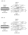
- An optical film 3 of the invention is, as shown in FIG. 1 , a laminate obtained by laminating a retardation film 2 onto a polarizing plate 1.
- the polarizing plate 1 that is used is a laminate obtained by laminating a transparent protective film 1b on both surfaces of a polarizer 1a. It is an example in which a retardation film 2 is laminated onto one surface thereof.
- the polarizing plate 1 and the retardation film 2 are laminated one on the other so that an absorption axis of the polarizing plate 1 and a slow axis of the retardation film 2 are perpendicular or parallel to each other.
- FIG. 1 a laminate obtained by laminating a retardation film 2 onto a polarizing plate 1.
- the polarizing plate 1 that is used is a laminate obtained by laminating a transparent protective film 1b on both surfaces of a polarizer 1a. It is an example in which a retardation film 2 is laminated onto one surface thereof.
- FIG. 1(A) shows a case where the absorption axis of the polarizing plate 1 and the slow axis of the retardation film 2 are laminated so as to be perpendicular to each other.
- FIG. 1(B) shows a case where the absorption axis of the polarizing plate 1 and the slow axis of the retardation film 2 are laminated so as to be parallel to each other.
- Isocyanate based adhesives polyvinyl alcohol based adhesives, gelatin based adhesives, vinyl based latex based, aqueous polyester based adhesives, and etc. may be used for adhesion processing for the above-mentioned polarizers and transparent protective films.
- the optical films 3 are laminates each obtained by laminating a polarizing plate 1 and a retardation film 2 so that the absorption axis of the polarizing plate 1 and the slow axis of the retardation film 2 are parallel to each other.
- the absorption axes of the optical films 3 (the polarizing plates 1) disposed on respective both sides of the liquid crystal cell 4 at the substrates thereof are arranged to be perpendicular to each other.
- the optical films 3 are, as shown in FIG.
- a retardation plate that works as a quarter wavelength plate in a wide wavelength ranges, such as a visible-light region, is obtained by a method in which a retardation layer working as a quarter wavelength plate to a pale color light with a wavelength of 550 nm is laminated with a retardation layer having other retardation characteristics, such as a retardation layer working as a half-wavelength plate. Therefore, the retardation plate located between a polarizing plate and a brightness enhancement film may consist of one or more retardation layers.
- the retardation films (X 2 ) and (Y 2 ) were laminated onto the respective polarizing plates prepared in example 3 with a pressure sensitive adhesive so that the slow axes of the retardation films (X 2 ) and (Y 2 ) were parallel with the absorption axes of the respective polarizing plates to thereby prepare optical films (X 2 ) and (Y 2 ).
- the retardation films (X 3 ) and (Y 3 ) were laminated onto the respective polarizing plates prepared in example 3 with a pressure sensitive adhesive so that the slow axes of the retardation films (X 3 ) and (Y 3 ) were parallel with the absorption axes of the respective polarizing plates to thereby prepare optical films (X 3 ) and (Y 3 ).
- the liquid crystal display was placed on the backlight and a contrast ratio was measured at an azimuth angle of 45 degrees relative to an optical axes perpendicular to each other of the polarizing plates and an inclination from a normal direction of 70 degrees to thereby obtain a contrast ratio of 50.
- the invention is useful as an optical film and the optical film is suited for use in a liquid crystal display driving in IPS mode, and especially for use in a transmissive liquid crystal display.
Landscapes
- Physics & Mathematics (AREA)
- Nonlinear Science (AREA)
- General Physics & Mathematics (AREA)
- Optics & Photonics (AREA)
- Mathematical Physics (AREA)
- Chemical & Material Sciences (AREA)
- Crystallography & Structural Chemistry (AREA)
- Liquid Crystal (AREA)
- Engineering & Computer Science (AREA)
- Mechanical Engineering (AREA)
- Geometry (AREA)
- Polarising Elements (AREA)
Claims (10)
- Optische Folie (3) für ein Flüssigkristalldisplay, erhalten durch Laminieren einer Polarisationsplatte (1) und einer Verzögerungsfolie (2), so daß eine Absorptionsachse der Polarisationsplatte (1) und eine slow-axis der Verzögerungsfolie (2) senkrecht oder parallel zueinander sind,
wobei die Polarisationsplatte (1) eine transparente Schutzfolie (1 b) auf beiden Oberflächen eines Polarisators (1 a) umfaßt, und, wenn eine Richtung auf der transparenten Schutzfolie (1 b), in welcher ein Brechungsindex innerhalb der Ebene maximiert ist, die X-Achse ist, eine Richtung senkrecht zu der X-Achse die Y-Achse ist, eine Richtung der Foliendicke die Z-Achse ist; und die Brechungsindices bei 550 nm in den jeweiligen Achsenrichtungen nx1, ny1 und nz1 sind; und eine Dicke der Schutzfolie definitionsgemäß d1 (nm) ist,
ein Verzögerung innerhalb der Ebene
einer Dickenrichtungsverzögerung wobei, wenn eine Richtung auf der Verzögerungsfolie (2), in welcher ein Brechungsindex innerhalb der Ebene maximiert ist, die X-Achse ist, eine Richtung senkrecht zu der X-Achse die Y-Achse ist,eine Richtung der Foliendicke die Z-Achse ist; und die Brechungsindices bei 550 nm in den jeweiligen Achsenrichtungen nx2, ny2 und nz2 sind; und eine Dicke der Verzögerungsfolie definitionsgemäß d2 (nm) ist, wobei die folgenden Beziehungen erfüllt sind:ein Nz-Wert, dargestellt durch
 ein Verzögerung innerhalb der Ebene
- Optische Folie nach Anspruch 1, aufgebracht auf ein IPS-Modus-Flüssigkristalldisplay, umfassend eine Flüssigkristallzelle, die im IPS-Modus betrieben wird.
- Optische Folie nach Anspruch 2, wobei die Flüssigkristallzelle, die im IPS-Modus betrieben wird, eine Flüssigkristallzelle im IPS-Modus mit einem Verzögerungswert in dem Bereich von 230 bis 360 nm bei 550 nm, wenn keine Spannung angelegt ist, ist.
- Durchlässiges Flüssigkristalldisplay, umfassend eine Flüssigkristallzelle (4), enthaltend ein Paar von Substraten, zwischen welchen eine Flüssigkristallschicht eingeschoben ist, und welche im IPS-Modus betrieben wird; und ein Paar von Polarisationsplatten (1), angeordnet auf beiden Seiten der Flüssigkristallzellen (4), so daß die Absorptionsachsen der Polarisationsplatten (1) senkrecht zueinander sind,
wobei mindestens eine der Polarisationsplatten (1) eine optische Folie nach Anspruch 2 oder 3 ist, und die optische Folie (3) derart angeordnet ist, daß eine Verzögerungsfolienseite der Flüssigkristallzelle (4) gegenüber angeordnet ist. - Durchlässiges Flüssigkristalldisplay nach Anspruch 4, wobei die optische Folie nach Anspruch 2 oder 3 auf einem Zellensubstrat auf der Beobachtungsseite angeordnet ist, und eine außergewöhnliche Brechungsindexrichtung eines Flüssigkristallmaterials in der Flüssigkristallzelle, wenn keine Spannung angelegt ist, und eine Absorptionsachse der Polarisationsplatte auf der Lichteinfallsseite parallel zueinander sind.
- Durchlässiges Flüssigkristalldisplay nach Anspruch 4, wobei die optische Folie nach Anspruch 2 oder 3 auf einem Zellensubstrat auf der Lichteinfallsseite angeordnet ist, und eine außergewöhnliche Brechungsindexrichtung eines Flüssigkristallmaterials in der Flüssigkristallzelle, wenn keine Spannung angelegt ist, und eine Absorptionsachse der Polarisationsplatte in der optischen Folie senkrecht zueinander sind.
- Durchlässiges Flüssigkristalldisplay nach Anspruch 5 oder 6, wobei die optische Folie eine Polarisationsplatte und eine Verzögerungsfolie umfaßt, so daß eine Absorptionsachse der Polarisationsplatte und eine slow-axis der Verzögerungsfolie senkrecht zueinander sind.
- Durchlässiges Flüssigkristalldisplay nach Anspruch 4, wobei die optische Folie nach Anspruch 2 oder 3 auf einem Zellensubstrat auf der Beobachtungsseite und der Lichteinfallsseite angeordnet ist, und eine außergewöhnliche Barechungsindexrichtung eines Flüssigkristallmaterials in der Flüssigkristallzelle, wenn keine Spannung angelegt ist, und eine Absorptionsachse der Polarisationsplatte in der optischen Folie auf der Lichteinfallsseite parallel zueinander sind.
- Durchlässiges Flüssigkristalldisplay nach Anspruch 8, wobei die optische Folie eine Polarisationsplatte und eine Verzögerungsfolie umfaßt, so daß eine Absorptionsachse der Polarisationsplatte und eine slow-axis der Verzögerungsfolie parallel zueinander sind.
- Durchlässiges Flüssigkristalldisplay nach Anspruch 8 oder 9, wobei eine Verzögerung in der Ebene Re2 der Verzögerungsfolie in der optischen Folie, die auf dem Zellensubstrat auf der Lichteinfallsseite angeordnet ist, kleiner als eine Verzögerung in der Ebene Re2 der Verzögerungsfolie in der optischen Folie, die auf dem Zellensubstrat auf der Beobachtungsseite angeordnet ist, ist.
Applications Claiming Priority (3)
| Application Number | Priority Date | Filing Date | Title |
|---|---|---|---|
| JP2002299938 | 2002-10-15 | ||
| JP2002299938 | 2002-10-15 | ||
| PCT/JP2003/012383 WO2004036273A1 (ja) | 2002-10-15 | 2003-09-29 | 光学フィルムおよび液晶表示装置 |
Publications (3)
| Publication Number | Publication Date |
|---|---|
| EP1553432A1 EP1553432A1 (de) | 2005-07-13 |
| EP1553432A4 EP1553432A4 (de) | 2007-08-22 |
| EP1553432B1 true EP1553432B1 (de) | 2009-09-09 |
Family
ID=32104969
Family Applications (1)
| Application Number | Title | Priority Date | Filing Date |
|---|---|---|---|
| EP03808892A Expired - Lifetime EP1553432B1 (de) | 2002-10-15 | 2003-09-29 | Optischer film und flüssigkristallanzeige |
Country Status (9)
| Country | Link |
|---|---|
| US (1) | US7388636B2 (de) |
| EP (1) | EP1553432B1 (de) |
| JP (2) | JP3687854B2 (de) |
| KR (2) | KR100757718B1 (de) |
| CN (2) | CN100510805C (de) |
| AT (1) | ATE442598T1 (de) |
| DE (1) | DE60329207D1 (de) |
| TW (1) | TWI279609B (de) |
| WO (1) | WO2004036273A1 (de) |
Families Citing this family (57)
| Publication number | Priority date | Publication date | Assignee | Title |
|---|---|---|---|---|
| US6642981B1 (en) * | 1996-09-30 | 2003-11-04 | Fujitsu Display Technologies Corporation | Liquid crystal display device operating in a vertically aligned mode including at least one retardation film |
| TWI242083B (en) | 2003-08-11 | 2005-10-21 | Sony Corp | Liquid crystal display device |
| JP4564795B2 (ja) * | 2003-09-30 | 2010-10-20 | 株式会社日立製作所 | 液晶表示装置 |
| KR100601916B1 (ko) * | 2003-11-21 | 2006-07-14 | 주식회사 엘지화학 | 양의 이축성 위상차 필름을 이용한 시야각 보상필름을포함하는 면상 스위칭 액정 표시장치 |
| TWI255947B (en) * | 2004-01-09 | 2006-06-01 | Chi Mei Optoelectronics Corp | Liquid crystal display device |
| JP4383903B2 (ja) * | 2004-01-23 | 2009-12-16 | 株式会社 日立ディスプレイズ | 偏光板及びそれを用いた液晶表示装置 |
| US7400371B2 (en) | 2004-02-03 | 2008-07-15 | Sumitomo Chemical Company, Limited | Liquid crystal display having particular retardation plate |
| TWI268372B (en) | 2004-03-26 | 2006-12-11 | Nitto Denko Corp | IPS mode liquid crystal display to realize a high contrast ratio over a wide range by laminating a polarizing plate and a retardation film to form an optical film |
| JP2005283846A (ja) * | 2004-03-29 | 2005-10-13 | Nitto Denko Corp | 光学フィルムおよび液晶表示装置 |
| JP4624129B2 (ja) * | 2004-04-27 | 2011-02-02 | 富士フイルム株式会社 | 液晶表示装置 |
| US7365815B2 (en) * | 2004-06-16 | 2008-04-29 | Sumitomo Chemical Company, Limited | Phase retardation film and liquid crystal display device including the same |
| JP2006018185A (ja) * | 2004-07-05 | 2006-01-19 | Nec Lcd Technologies Ltd | 液晶表示装置 |
| JP4907881B2 (ja) | 2004-09-09 | 2012-04-04 | 富士フイルム株式会社 | 液晶組成物、光学補償フィルム、及び液晶表示装置 |
| JP2006106180A (ja) * | 2004-10-01 | 2006-04-20 | Nitto Denko Corp | 光学フィルムおよび画像表示装置 |
| KR100682230B1 (ko) * | 2004-11-12 | 2007-02-12 | 주식회사 엘지화학 | 수직 배향 액정표시장치 |
| JP3851919B2 (ja) | 2004-12-20 | 2006-11-29 | 日東電工株式会社 | 液晶パネルおよび液晶表示装置 |
| JP5076302B2 (ja) * | 2005-01-25 | 2012-11-21 | 住友化学株式会社 | 液晶表示装置及びそれに有用な偏光板のセット |
| JP4697775B2 (ja) * | 2005-01-31 | 2011-06-08 | 日東電工株式会社 | 液晶パネルおよび液晶表示装置 |
| JP4536543B2 (ja) * | 2005-02-08 | 2010-09-01 | 株式会社 日立ディスプレイズ | 液晶表示装置 |
| JP2006251439A (ja) * | 2005-03-11 | 2006-09-21 | Nitto Denko Corp | 液晶パネル、液晶テレビおよび液晶表示装置 |
| JP3972371B2 (ja) * | 2005-03-15 | 2007-09-05 | ソニー株式会社 | 位相差補償板、位相差補償器、液晶表示装置および投射型画像表示装置 |
| JP2006267625A (ja) * | 2005-03-24 | 2006-10-05 | Nitto Denko Corp | 液晶パネル、液晶テレビおよび液晶表示装置 |
| JP4792777B2 (ja) | 2005-03-25 | 2011-10-12 | 東ソー株式会社 | 広視野角補償フィルム及びそれを用いてなる透過型液晶表示装置 |
| JP4778718B2 (ja) * | 2005-03-28 | 2011-09-21 | 帝人株式会社 | 液晶表示装置およびそれに用いられる負の略1軸性光学フィルム |
| KR20080008346A (ko) * | 2005-03-30 | 2008-01-23 | 다이니폰 인사츠 가부시키가이샤 | 편광판 |
| JP2007003917A (ja) * | 2005-06-24 | 2007-01-11 | Konica Minolta Opto Inc | 透過型液晶表示装置 |
| JP2007017816A (ja) * | 2005-07-11 | 2007-01-25 | Okura Ind Co Ltd | 熱可塑性ノルボルネン系樹脂からなる光学補償フィルム |
| JP2007024940A (ja) * | 2005-07-12 | 2007-02-01 | Tosoh Corp | 広視野角補償フィルムおよびそれを用いてなる液晶表示装置 |
| KR101277548B1 (ko) * | 2005-08-08 | 2013-06-21 | 삼성디스플레이 주식회사 | 편광필름 및 이를 포함한 표시 장치 |
| JP2007147884A (ja) * | 2005-11-25 | 2007-06-14 | Nitto Denko Corp | 液晶表示装置 |
| JP2007218940A (ja) * | 2006-02-14 | 2007-08-30 | Epson Imaging Devices Corp | 液晶装置及び電子機器 |
| US9011991B2 (en) * | 2006-03-24 | 2015-04-21 | Zeon Corporation | Lengthy stretched film, and manufacturing method and use thereof |
| JP2007279127A (ja) * | 2006-04-03 | 2007-10-25 | Nitto Denko Corp | 液晶パネル、液晶テレビ、および液晶表示装置 |
| JP2008058893A (ja) * | 2006-09-04 | 2008-03-13 | Konica Minolta Opto Inc | セルロースエステルフィルム、偏光板保護フィルム、偏光板、セルロースエステルフィルムの製造方法および液晶表示装置 |
| KR101337705B1 (ko) * | 2006-10-05 | 2013-12-06 | 코니카 미놀타 어드밴스드 레이어즈 인코포레이티드 | 횡전계 스위칭 모드형 액정 표시 장치 |
| KR20080034405A (ko) * | 2006-10-16 | 2008-04-21 | 다이니폰 인사츠 가부시키가이샤 | 위상차 필름 및 편광판 |
| TWI407197B (zh) * | 2006-11-20 | 2013-09-01 | Lg Chemical Ltd | 光學膜以及彼之製法 |
| JP5202889B2 (ja) | 2007-06-29 | 2013-06-05 | 日東電工株式会社 | 積層偏光板およびその製造方法ならびに液晶表示装置 |
| JP2009192866A (ja) | 2008-02-15 | 2009-08-27 | Epson Imaging Devices Corp | 液晶装置及び電子機器 |
| JP2009265598A (ja) * | 2008-03-31 | 2009-11-12 | Fujifilm Corp | 偏光板用保護フィルム |
| JP5274929B2 (ja) * | 2008-08-05 | 2013-08-28 | 日東電工株式会社 | 液晶パネル及び液晶表示装置 |
| JP2010078678A (ja) | 2008-09-24 | 2010-04-08 | Hitachi Displays Ltd | 表示装置 |
| JP5235755B2 (ja) | 2008-09-26 | 2013-07-10 | 富士フイルム株式会社 | アクリルフィルム、光学補償フィルム、及びそれを用いたips又はffsモード液晶表示装置 |
| JP4689769B1 (ja) * | 2009-12-03 | 2011-05-25 | シャープ株式会社 | 液晶表示装置 |
| JP5538853B2 (ja) * | 2009-12-10 | 2014-07-02 | 富士フイルム株式会社 | 液晶表示装置 |
| JP5491966B2 (ja) * | 2010-05-28 | 2014-05-14 | 株式会社ジャパンディスプレイ | 液晶表示装置 |
| JP2012177907A (ja) * | 2011-02-01 | 2012-09-13 | Fujifilm Corp | 液晶表示装置 |
| JP2013254043A (ja) * | 2012-06-05 | 2013-12-19 | Jiroo Corporate Plan:Kk | 位相差フィルム、位相差フィルムの製造方法及び偏光板 |
| JP2014102521A (ja) * | 2014-01-24 | 2014-06-05 | Japan Display Inc | 液晶装置及び電子機器 |
| KR101943692B1 (ko) * | 2015-11-04 | 2019-01-29 | 삼성에스디아이 주식회사 | 편광판 및 이를 포함하는 액정 표시 장치 |
| JP6065144B1 (ja) * | 2016-04-25 | 2017-01-25 | 大日本印刷株式会社 | 調光フィルム |
| KR102118016B1 (ko) | 2016-06-24 | 2020-06-02 | 닛토덴코 가부시키가이샤 | 장척 광학 필름 적층체, 장척 광학 필름 적층체의 롤 및 ips 액정 표시 장치 |
| CN106526920B (zh) * | 2016-12-29 | 2019-08-20 | 深圳市华星光电技术有限公司 | 液晶显示补偿膜面内相位差值测量方法及装置 |
| CN116261682A (zh) * | 2020-09-30 | 2023-06-13 | 富士胶片株式会社 | 光学元件 |
| JP7802473B2 (ja) * | 2021-09-01 | 2026-01-20 | 日東電工株式会社 | 位相差層付偏光板および画像表示装置 |
| JP7684181B2 (ja) * | 2021-10-04 | 2025-05-27 | 日東電工株式会社 | 位相差層付偏光板および画像表示装置 |
| JP7684180B2 (ja) * | 2021-10-04 | 2025-05-27 | 日東電工株式会社 | 位相差層付偏光板および画像表示装置 |
Family Cites Families (5)
| Publication number | Priority date | Publication date | Assignee | Title |
|---|---|---|---|---|
| JP3165168B2 (ja) | 1991-04-02 | 2001-05-14 | 日東電工株式会社 | 偏光板及び液晶表示装置 |
| JP3165178B2 (ja) | 1991-06-19 | 2001-05-14 | 日東電工株式会社 | 偏光板及び液晶表示装置 |
| JP2982869B2 (ja) * | 1998-04-16 | 1999-11-29 | インターナショナル・ビジネス・マシーンズ・コーポレイション | 液晶表示装置 |
| JP4566385B2 (ja) * | 2000-10-30 | 2010-10-20 | 日東電工株式会社 | 偏光板 |
| JP2002258041A (ja) * | 2001-03-01 | 2002-09-11 | Nitto Denko Corp | 光学補償偏光板及び液晶表示装置 |
-
2003
- 2003-09-25 JP JP2003333597A patent/JP3687854B2/ja not_active Expired - Fee Related
- 2003-09-29 KR KR1020057005767A patent/KR100757718B1/ko not_active Expired - Fee Related
- 2003-09-29 CN CNB038242877A patent/CN100510805C/zh not_active Expired - Lifetime
- 2003-09-29 KR KR1020077006193A patent/KR100750845B1/ko not_active Expired - Fee Related
- 2003-09-29 EP EP03808892A patent/EP1553432B1/de not_active Expired - Lifetime
- 2003-09-29 AT AT03808892T patent/ATE442598T1/de not_active IP Right Cessation
- 2003-09-29 WO PCT/JP2003/012383 patent/WO2004036273A1/ja not_active Ceased
- 2003-09-29 TW TW092126870A patent/TWI279609B/zh not_active IP Right Cessation
- 2003-09-29 US US10/531,326 patent/US7388636B2/en not_active Expired - Lifetime
- 2003-09-29 CN CNB200610164161XA patent/CN100424564C/zh not_active Expired - Lifetime
- 2003-09-29 DE DE60329207T patent/DE60329207D1/de not_active Expired - Lifetime
-
2004
- 2004-11-30 JP JP2004346780A patent/JP3969591B2/ja not_active Expired - Fee Related
Also Published As
| Publication number | Publication date |
|---|---|
| DE60329207D1 (de) | 2009-10-22 |
| KR20070041634A (ko) | 2007-04-18 |
| CN1963635A (zh) | 2007-05-16 |
| CN1688906A (zh) | 2005-10-26 |
| KR100757718B1 (ko) | 2007-09-11 |
| KR20050071540A (ko) | 2005-07-07 |
| KR100750845B1 (ko) | 2007-08-22 |
| US20060164579A1 (en) | 2006-07-27 |
| JP3969591B2 (ja) | 2007-09-05 |
| JP3687854B2 (ja) | 2005-08-24 |
| WO2004036273A1 (ja) | 2004-04-29 |
| JP2005173588A (ja) | 2005-06-30 |
| ATE442598T1 (de) | 2009-09-15 |
| EP1553432A4 (de) | 2007-08-22 |
| JP2004157523A (ja) | 2004-06-03 |
| TW200411250A (en) | 2004-07-01 |
| EP1553432A1 (de) | 2005-07-13 |
| CN100424564C (zh) | 2008-10-08 |
| CN100510805C (zh) | 2009-07-08 |
| US7388636B2 (en) | 2008-06-17 |
| TWI279609B (en) | 2007-04-21 |
Similar Documents
| Publication | Publication Date | Title |
|---|---|---|
| EP1553432B1 (de) | Optischer film und flüssigkristallanzeige | |
| US7075604B2 (en) | Optical film and display system | |
| US7586569B2 (en) | IPS mode liquid crystal display | |
| US7042540B2 (en) | Optical film and display system | |
| US7466382B2 (en) | Optical film and image display | |
| US7466381B2 (en) | Optical film and image viewing display | |
| KR100908773B1 (ko) | 타원 편광판 및 액정 표시 장치 | |
| JP2004004641A (ja) | 光学フィルムおよび画像表示装置 | |
| US20080074585A1 (en) | Liquid crystal panel and liquid crystal display device | |
| JP2004004642A (ja) | 光学フィルムおよび画像表示装置 | |
| US20070195244A1 (en) | Optical Film And Image Display | |
| JP2005309386A (ja) | Ipsモード液晶表示装置 | |
| JP2004325468A (ja) | 偏光板、その製造方法、光学フィルムおよび画像表示装置 | |
| JP2007264235A (ja) | Ipsモード液晶表示装置 |
Legal Events
| Date | Code | Title | Description |
|---|---|---|---|
| PUAI | Public reference made under article 153(3) epc to a published international application that has entered the european phase |
Free format text: ORIGINAL CODE: 0009012 |
|
| 17P | Request for examination filed |
Effective date: 20050421 |
|
| AK | Designated contracting states |
Kind code of ref document: A1 Designated state(s): AT BE BG CH CY CZ DE DK EE ES FI FR GB GR HU IE IT LI LU MC NL PT RO SE SI SK TR |
|
| A4 | Supplementary search report drawn up and despatched |
Effective date: 20070720 |
|
| 17Q | First examination report despatched |
Effective date: 20071008 |
|
| GRAP | Despatch of communication of intention to grant a patent |
Free format text: ORIGINAL CODE: EPIDOSNIGR1 |
|
| GRAS | Grant fee paid |
Free format text: ORIGINAL CODE: EPIDOSNIGR3 |
|
| GRAA | (expected) grant |
Free format text: ORIGINAL CODE: 0009210 |
|
| AK | Designated contracting states |
Kind code of ref document: B1 Designated state(s): AT BE BG CH CY CZ DE DK EE ES FI FR GB GR HU IE IT LI LU MC NL PT RO SE SI SK TR |
|
| REG | Reference to a national code |
Ref country code: GB Ref legal event code: FG4D |
|
| REG | Reference to a national code |
Ref country code: CH Ref legal event code: EP |
|
| REG | Reference to a national code |
Ref country code: IE Ref legal event code: FG4D |
|
| REF | Corresponds to: |
Ref document number: 60329207 Country of ref document: DE Date of ref document: 20091022 Kind code of ref document: P |
|
| PG25 | Lapsed in a contracting state [announced via postgrant information from national office to epo] |
Ref country code: SE Free format text: LAPSE BECAUSE OF FAILURE TO SUBMIT A TRANSLATION OF THE DESCRIPTION OR TO PAY THE FEE WITHIN THE PRESCRIBED TIME-LIMIT Effective date: 20090909 Ref country code: FI Free format text: LAPSE BECAUSE OF FAILURE TO SUBMIT A TRANSLATION OF THE DESCRIPTION OR TO PAY THE FEE WITHIN THE PRESCRIBED TIME-LIMIT Effective date: 20090909 |
|
| NLV1 | Nl: lapsed or annulled due to failure to fulfill the requirements of art. 29p and 29m of the patents act | ||
| PG25 | Lapsed in a contracting state [announced via postgrant information from national office to epo] |
Ref country code: NL Free format text: LAPSE BECAUSE OF FAILURE TO SUBMIT A TRANSLATION OF THE DESCRIPTION OR TO PAY THE FEE WITHIN THE PRESCRIBED TIME-LIMIT Effective date: 20090909 Ref country code: SI Free format text: LAPSE BECAUSE OF FAILURE TO SUBMIT A TRANSLATION OF THE DESCRIPTION OR TO PAY THE FEE WITHIN THE PRESCRIBED TIME-LIMIT Effective date: 20090909 |
|
| PG25 | Lapsed in a contracting state [announced via postgrant information from national office to epo] |
Ref country code: CY Free format text: LAPSE BECAUSE OF FAILURE TO SUBMIT A TRANSLATION OF THE DESCRIPTION OR TO PAY THE FEE WITHIN THE PRESCRIBED TIME-LIMIT Effective date: 20090909 |
|
| PG25 | Lapsed in a contracting state [announced via postgrant information from national office to epo] |
Ref country code: PT Free format text: LAPSE BECAUSE OF FAILURE TO SUBMIT A TRANSLATION OF THE DESCRIPTION OR TO PAY THE FEE WITHIN THE PRESCRIBED TIME-LIMIT Effective date: 20100111 Ref country code: RO Free format text: LAPSE BECAUSE OF FAILURE TO SUBMIT A TRANSLATION OF THE DESCRIPTION OR TO PAY THE FEE WITHIN THE PRESCRIBED TIME-LIMIT Effective date: 20090909 Ref country code: ES Free format text: LAPSE BECAUSE OF FAILURE TO SUBMIT A TRANSLATION OF THE DESCRIPTION OR TO PAY THE FEE WITHIN THE PRESCRIBED TIME-LIMIT Effective date: 20091220 Ref country code: MC Free format text: LAPSE BECAUSE OF NON-PAYMENT OF DUE FEES Effective date: 20090930 Ref country code: EE Free format text: LAPSE BECAUSE OF FAILURE TO SUBMIT A TRANSLATION OF THE DESCRIPTION OR TO PAY THE FEE WITHIN THE PRESCRIBED TIME-LIMIT Effective date: 20090909 Ref country code: CZ Free format text: LAPSE BECAUSE OF FAILURE TO SUBMIT A TRANSLATION OF THE DESCRIPTION OR TO PAY THE FEE WITHIN THE PRESCRIBED TIME-LIMIT Effective date: 20090909 |
|
| REG | Reference to a national code |
Ref country code: CH Ref legal event code: PL |
|
| PG25 | Lapsed in a contracting state [announced via postgrant information from national office to epo] |
Ref country code: SK Free format text: LAPSE BECAUSE OF FAILURE TO SUBMIT A TRANSLATION OF THE DESCRIPTION OR TO PAY THE FEE WITHIN THE PRESCRIBED TIME-LIMIT Effective date: 20090909 |
|
| PG25 | Lapsed in a contracting state [announced via postgrant information from national office to epo] |
Ref country code: AT Free format text: LAPSE BECAUSE OF FAILURE TO SUBMIT A TRANSLATION OF THE DESCRIPTION OR TO PAY THE FEE WITHIN THE PRESCRIBED TIME-LIMIT Effective date: 20090909 Ref country code: BE Free format text: LAPSE BECAUSE OF FAILURE TO SUBMIT A TRANSLATION OF THE DESCRIPTION OR TO PAY THE FEE WITHIN THE PRESCRIBED TIME-LIMIT Effective date: 20090909 |
|
| PLBE | No opposition filed within time limit |
Free format text: ORIGINAL CODE: 0009261 |
|
| STAA | Information on the status of an ep patent application or granted ep patent |
Free format text: STATUS: NO OPPOSITION FILED WITHIN TIME LIMIT |
|
| PG25 | Lapsed in a contracting state [announced via postgrant information from national office to epo] |
Ref country code: DK Free format text: LAPSE BECAUSE OF FAILURE TO SUBMIT A TRANSLATION OF THE DESCRIPTION OR TO PAY THE FEE WITHIN THE PRESCRIBED TIME-LIMIT Effective date: 20090909 Ref country code: IE Free format text: LAPSE BECAUSE OF NON-PAYMENT OF DUE FEES Effective date: 20090929 |
|
| 26N | No opposition filed |
Effective date: 20100610 |
|
| GBPC | Gb: european patent ceased through non-payment of renewal fee |
Effective date: 20091209 |
|
| PG25 | Lapsed in a contracting state [announced via postgrant information from national office to epo] |
Ref country code: GR Free format text: LAPSE BECAUSE OF FAILURE TO SUBMIT A TRANSLATION OF THE DESCRIPTION OR TO PAY THE FEE WITHIN THE PRESCRIBED TIME-LIMIT Effective date: 20091210 Ref country code: CH Free format text: LAPSE BECAUSE OF NON-PAYMENT OF DUE FEES Effective date: 20090930 Ref country code: LI Free format text: LAPSE BECAUSE OF NON-PAYMENT OF DUE FEES Effective date: 20090930 |
|
| PG25 | Lapsed in a contracting state [announced via postgrant information from national office to epo] |
Ref country code: GB Free format text: LAPSE BECAUSE OF NON-PAYMENT OF DUE FEES Effective date: 20091209 |
|
| PG25 | Lapsed in a contracting state [announced via postgrant information from national office to epo] |
Ref country code: BG Free format text: LAPSE BECAUSE OF FAILURE TO SUBMIT A TRANSLATION OF THE DESCRIPTION OR TO PAY THE FEE WITHIN THE PRESCRIBED TIME-LIMIT Effective date: 20090930 Ref country code: IT Free format text: LAPSE BECAUSE OF FAILURE TO SUBMIT A TRANSLATION OF THE DESCRIPTION OR TO PAY THE FEE WITHIN THE PRESCRIBED TIME-LIMIT Effective date: 20090909 |
|
| PG25 | Lapsed in a contracting state [announced via postgrant information from national office to epo] |
Ref country code: LU Free format text: LAPSE BECAUSE OF NON-PAYMENT OF DUE FEES Effective date: 20090929 |
|
| REG | Reference to a national code |
Ref country code: FR Ref legal event code: ST Effective date: 20110502 |
|
| PG25 | Lapsed in a contracting state [announced via postgrant information from national office to epo] |
Ref country code: HU Free format text: LAPSE BECAUSE OF FAILURE TO SUBMIT A TRANSLATION OF THE DESCRIPTION OR TO PAY THE FEE WITHIN THE PRESCRIBED TIME-LIMIT Effective date: 20100310 |
|
| PG25 | Lapsed in a contracting state [announced via postgrant information from national office to epo] |
Ref country code: FR Free format text: LAPSE BECAUSE OF NON-PAYMENT OF DUE FEES Effective date: 20091109 |
|
| PG25 | Lapsed in a contracting state [announced via postgrant information from national office to epo] |
Ref country code: TR Free format text: LAPSE BECAUSE OF FAILURE TO SUBMIT A TRANSLATION OF THE DESCRIPTION OR TO PAY THE FEE WITHIN THE PRESCRIBED TIME-LIMIT Effective date: 20090909 |
|
| PGFP | Annual fee paid to national office [announced via postgrant information from national office to epo] |
Ref country code: DE Payment date: 20210818 Year of fee payment: 19 |
|
| REG | Reference to a national code |
Ref country code: DE Ref legal event code: R119 Ref document number: 60329207 Country of ref document: DE |
|
| PG25 | Lapsed in a contracting state [announced via postgrant information from national office to epo] |
Ref country code: DE Free format text: LAPSE BECAUSE OF NON-PAYMENT OF DUE FEES Effective date: 20230401 |