EP1552529B1 - Method and apparatus for erasing flash memory - Google Patents
Method and apparatus for erasing flash memory Download PDFInfo
- Publication number
- EP1552529B1 EP1552529B1 EP03756241A EP03756241A EP1552529B1 EP 1552529 B1 EP1552529 B1 EP 1552529B1 EP 03756241 A EP03756241 A EP 03756241A EP 03756241 A EP03756241 A EP 03756241A EP 1552529 B1 EP1552529 B1 EP 1552529B1
- Authority
- EP
- European Patent Office
- Prior art keywords
- erase
- source
- gate
- voltage
- negative voltage
- Prior art date
- Legal status (The legal status is an assumption and is not a legal conclusion. Google has not performed a legal analysis and makes no representation as to the accuracy of the status listed.)
- Expired - Lifetime
Links
- 230000015654 memory Effects 0.000 title claims abstract description 88
- 238000000034 method Methods 0.000 title claims abstract description 34
- 239000000758 substrate Substances 0.000 claims description 30
- 230000003071 parasitic effect Effects 0.000 claims description 20
- 238000007599 discharging Methods 0.000 claims description 12
- 230000014759 maintenance of location Effects 0.000 claims description 11
- 230000008878 coupling Effects 0.000 claims description 10
- 238000010168 coupling process Methods 0.000 claims description 10
- 238000005859 coupling reaction Methods 0.000 claims description 10
- 230000005641 tunneling Effects 0.000 claims description 8
- 125000006850 spacer group Chemical group 0.000 claims description 5
- 239000003990 capacitor Substances 0.000 claims description 4
- 230000033228 biological regulation Effects 0.000 claims description 3
- 230000003247 decreasing effect Effects 0.000 claims description 3
- 238000004519 manufacturing process Methods 0.000 claims description 3
- 230000003190 augmentative effect Effects 0.000 claims 1
- 230000003472 neutralizing effect Effects 0.000 abstract 1
- 108091006146 Channels Proteins 0.000 description 30
- VYPSYNLAJGMNEJ-UHFFFAOYSA-N Silicium dioxide Chemical compound O=[Si]=O VYPSYNLAJGMNEJ-UHFFFAOYSA-N 0.000 description 10
- 230000002829 reductive effect Effects 0.000 description 7
- 238000013459 approach Methods 0.000 description 5
- 238000013461 design Methods 0.000 description 5
- 238000009792 diffusion process Methods 0.000 description 5
- 239000000377 silicon dioxide Substances 0.000 description 5
- 230000007246 mechanism Effects 0.000 description 4
- 230000002441 reversible effect Effects 0.000 description 4
- 229910008062 Si-SiO2 Inorganic materials 0.000 description 2
- 229910006403 Si—SiO2 Inorganic materials 0.000 description 2
- 230000004888 barrier function Effects 0.000 description 2
- 230000008901 benefit Effects 0.000 description 2
- 230000000694 effects Effects 0.000 description 2
- 230000005684 electric field Effects 0.000 description 2
- 230000006870 function Effects 0.000 description 2
- 238000002347 injection Methods 0.000 description 2
- 239000007924 injection Substances 0.000 description 2
- 230000006386 memory function Effects 0.000 description 2
- 229910021420 polycrystalline silicon Inorganic materials 0.000 description 2
- 229920005591 polysilicon Polymers 0.000 description 2
- 230000008569 process Effects 0.000 description 2
- 235000012239 silicon dioxide Nutrition 0.000 description 2
- 238000012360 testing method Methods 0.000 description 2
- 230000001052 transient effect Effects 0.000 description 2
- 108010075750 P-Type Calcium Channels Proteins 0.000 description 1
- XUIMIQQOPSSXEZ-UHFFFAOYSA-N Silicon Chemical compound [Si] XUIMIQQOPSSXEZ-UHFFFAOYSA-N 0.000 description 1
- 238000009825 accumulation Methods 0.000 description 1
- 230000006978 adaptation Effects 0.000 description 1
- 230000002411 adverse Effects 0.000 description 1
- 230000006399 behavior Effects 0.000 description 1
- 238000010276 construction Methods 0.000 description 1
- 238000012937 correction Methods 0.000 description 1
- 238000013500 data storage Methods 0.000 description 1
- 230000003111 delayed effect Effects 0.000 description 1
- 238000010586 diagram Methods 0.000 description 1
- 230000002349 favourable effect Effects 0.000 description 1
- 230000005055 memory storage Effects 0.000 description 1
- 238000012544 monitoring process Methods 0.000 description 1
- 238000004321 preservation Methods 0.000 description 1
- 230000008672 reprogramming Effects 0.000 description 1
- 230000000717 retained effect Effects 0.000 description 1
- 229910052710 silicon Inorganic materials 0.000 description 1
- 239000010703 silicon Substances 0.000 description 1
- 239000000243 solution Substances 0.000 description 1
- 238000001228 spectrum Methods 0.000 description 1
- 230000001629 suppression Effects 0.000 description 1
Images


Classifications
-
- G—PHYSICS
- G11—INFORMATION STORAGE
- G11C—STATIC STORES
- G11C16/00—Erasable programmable read-only memories
- G11C16/02—Erasable programmable read-only memories electrically programmable
- G11C16/06—Auxiliary circuits, e.g. for writing into memory
- G11C16/10—Programming or data input circuits
- G11C16/14—Circuits for erasing electrically, e.g. erase voltage switching circuits
- G11C16/16—Circuits for erasing electrically, e.g. erase voltage switching circuits for erasing blocks, e.g. arrays, words, groups
-
- G—PHYSICS
- G11—INFORMATION STORAGE
- G11C—STATIC STORES
- G11C16/00—Erasable programmable read-only memories
- G11C16/02—Erasable programmable read-only memories electrically programmable
- G11C16/06—Auxiliary circuits, e.g. for writing into memory
- G11C16/10—Programming or data input circuits
- G11C16/14—Circuits for erasing electrically, e.g. erase voltage switching circuits
-
- G—PHYSICS
- G11—INFORMATION STORAGE
- G11C—STATIC STORES
- G11C16/00—Erasable programmable read-only memories
- G11C16/02—Erasable programmable read-only memories electrically programmable
- G11C16/06—Auxiliary circuits, e.g. for writing into memory
- G11C16/08—Address circuits; Decoders; Word-line control circuits
-
- H—ELECTRICITY
- H10—SEMICONDUCTOR DEVICES; ELECTRIC SOLID-STATE DEVICES NOT OTHERWISE PROVIDED FOR
- H10B—ELECTRONIC MEMORY DEVICES
- H10B69/00—Erasable-and-programmable ROM [EPROM] devices not provided for in groups H10B41/00 - H10B63/00, e.g. ultraviolet erasable-and-programmable ROM [UVEPROM] devices
Definitions
- the present invention relates in general to a method and apparatus for erasing of a non-volatile memory device and in particular to a method and apparatus for an erase operation of a memory array of a nonvolatile memory device that can reduce the number of trapped holes in the tunnel oxide of flash memory cells.
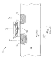
- Fig. 1 illustrates a cross sectional view of a conventional flash memory cell 100.
- Memory cell 100 includes a substrate 102, a source 104, a control gate 108, a floating gate 106 electrically isolated by an insulating layer of silicon dioxide (SiO 2 ) 110, and a drain 112.
- Memory cell 100 is thus basically an n-channel transistor with the addition of a floating gate. Electrical access to floating gate 106 takes place only through a capacitor network of surrounding SiO 2 layers and source 104, drain 112, channel 105, and control gate 108. Any charge present on the floating gate 106 is retained due to the inherent Si-SiO 2 energy barrier height, leading to the non-volatile nature of the memory cell.
- Programming a flash memory cell means that charge (i.e., electrons) is added to the floating gate 106.
- a high drain to source bias voltage is applied, along with a high control gate voltage.
- the gate voltage inverts the channel, while the drain bias accelerates electrons towards the drain.
- some electrons will experience a collision with the silicon lattice and become redirected towards the Si-SiO 2 interface.
- the gate voltage With the aid of the field produced by the gate voltage some of these electrons will travel across the oxide and become added to the floating gate.
- the electrons added to the floating gate increase the cell's threshold voltage. Programming is a selective operation, performed on each individual cell.
- Reading a flash memory cell takes place as follows. For cells that have been programmed, the turn-on voltage V t of cells is increased by the increased charge on the floating gate. By applying a control gate voltage and monitoring the drain current, differences between cells with charge and cells without charge on their floating gates can be determined.
- a sense amplifier compares cell drain current with that of a reference cell (typically a flash cell which is programmed to the reference level during manufacturing test). An erased cell has more cell current than the reference cell and therefore is a logical "1," while a programmed cell draws less current than the reference cell and is a logical "0.”
- Erasing a flash cell means that electrons (charge) are removed from the floating gate 106. Erasing flash memory is performed by applying electrical voltages to many cells at once so that the cells are erased in a "flash.” A typical erase operation in a flash memory may be performed by applying a positive voltage to the source 104, a negative or a ground voltage to the control gate 108, and holding substrate 102 of the memory cells at ground. The drain 112 is allowed to float. Under these conditions, a high electric field (8-10MV/cm) is present between the floating gate and the source. The source junction experiences a gated-diode condition during erase and electrons that manage to tunnel through the first few angstroms of the SiO 2 are then swept into the source. After the erase has been completed, electrons have been removed from the floating gate, reducing the cell threshold voltage Vt. While programming is selective to each individual cell, erase is not, with many cells being erased simultaneously.
- SILC Stress Induced leakage current
- Fig. 1 shows a conventional floating gate memory cell 100 including an n+ type source 104, a p type channel 105, an n+ type drain 112, and a p type substrate 102.
- a floating gate 106 is sandwiched between an insulating dielectric layer 110 and thin tunnel oxide 114 over channel 105.
- Floating gate 106 is the memory storage element in a flash memory and is electrically insulated from other elements of the memory cell.
- Control gate 108 is located on top of the insulating dielectric 110 and is positioned over floating gate 106.
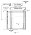
- Flash memory 200 includes a control circuit 202 for controlling the operations of the memory such as reading, writing and erasing, column decoder 204, sense amplifiers/bitline drivers 206, column multiplexer 218, wordlines 212, memory array 210, bitlines 208, and row decoder 214 with wordline drivers 216.
- control circuit 202 for controlling the operations of the memory such as reading, writing and erasing, column decoder 204, sense amplifiers/bitline drivers 206, column multiplexer 218, wordlines 212, memory array 210, bitlines 208, and row decoder 214 with wordline drivers 216.
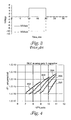
- FIG. 3 An example of the sequence of voltage pulses for a conventional flash memory erase operation is illustrated in Fig. 3 .
- the source-drain voltage is increased to about 5 to 6 V while at the same time the gate-substrate voltage is decreased to about -10 V. This potential difference is held for about 10 ms and then abruptly discharged to zero.
- the combination of voltage values induces an electric field across tunnel oxide 114 between floating gate 106 and source 104, resulting in tunneling that drives electrons off floating gate 106 and effectively erases the memory cell.
- the reverse bias on the junction between body 102 and source 104 injects holes into tunnel oxide 114 and some of these holes become trapped in tunnel oxide 114.
- the holes trapped in tunnel oxide 114 may effectively reduce the barrier for low-field electron injection from floating gate 106 into tunnel oxide 114, thus causing SILC and SILC-related charge loss or gain for the flash cell.
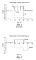
- Curve 201 shows the tunnel I-V characteristics (IP1 vs. VP1) for a fresh, unstressed array in a voltage sweep (V-sweep) of the polysilicon 1 gate of the flash memory cells of the array at negative voltage with the substrate and source at ground.
- V-sweep voltage sweep
- Curve 202 shows the result of stressing, i.e., application of successive erase-program cycles on an array of floating gate cells.
- stressing is simulated by a constant voltage stress in which the gate-substrate is held at -10V and the source-substrate is held at 6 V, a high reverse junction bias, for 200 seconds.
- Curve 202 shows that onset of leakage current will occur at an abnormally low voltage of about -7V, after stressing the array.
- Curves 203, 204 and 205 show successive V-sweeps where the stress voltage has been removed, the gate voltage successively swept to further negative values, and the substrate and source are held at ground.
- Curves 203, 204 and 205 demonstrate that the SILC is suppressed and the onset of tunneling is advantageously shifted to a higher negative gate-substrate voltage after the array has been subjected to gate V-sweeps at zero voltage across the source-substrate junction. In each successive V-sweep curve, the onset of tunneling is pushed back to a higher voltage, and thus, SILC is more effectively suppressed.
- SILC is created and/or enhanced when the gated source diode is subjected to high reverse bias and there is low tunneling current across the gate oxide. These conditions are favorable for hole generation and injection into the gate oxide. On the other hand, SILC may be suppressed when the gated source diode is subjected to a high electron tunneling current across the gate oxide at zero or low reverse current bias for the source junction.
- One possible way to neutralize holes trapped in the tunnel oxide during an erase pulse is to apply a condition of uniform tunneling at high negative gate and low or zero positive source voltage at the end of the erase pulse.
- This Prior Art approach is illustrated in Fig. 5 .
- two positive 6 V pulses of about 3 ms are applied to the source (Vs) over a 10 ms erase period.
- a positive 6 V pulse is also applied to the substrate (Vsub) concurrent with the second positive source pulse.
- the gate-substrate voltage (VG) is held at negative 10V for the entire 10ms period.
- Application of a positive voltage pulse on the substrate allows the erase operation to be done in a single step channel erase. However, this also requires the added complexity of building the memory array inside a triple well.
- a channel erase condition may also be realized by applying an additional voltage pulse of higher negative value to the gate (wordlines) while the source is biased at the same potential as the substrate (ground), after the regular erase pulse.
- This procedure is illustrated in Fig. 6 .
- a positive pulse of about 5V is applied between source and substrate for a period of about 10 ms.
- the gate substrate voltage is taken to negative 10V.
- the voltage between the gate and substrate is increased to negative 15 volts and held at that potential for an additional 5 ms. While this approach can be implemented on a flash memory without a triple well surrounding the array, it has the disadvantage of requiring extra erase time and the supply of a higher negative voltage.
- a more convenient approach, illustrated in Fig. 7A is to discharge the source toward the substrate potential (or other area of common voltage) at the end of the regular erase pulse, while the negative voltage to the control gate (wordlines) is maintained.
- a positive pulse of about 5V is applied between source and substrate for about 10 ms.
- the gate-substrate voltage is brought to negative 10 V and held for the 10 ms period.
- the source-substrate potential is discharged rapidly, in a fraction of a millisecond, but the discharge of negative gate-substrate voltage is delayed for a time in the range of 1-100 ms.
- Fig. 7A depicts the expected behavior for the gate voltage VGSub if the forced discharge of the source VSSub takes place in a time of a fraction of 1 millisecond or faster.
- the amount of the excess negative gate voltage and its gradual decrease on the waveform for VGSub after the discharge of the source (VSSub) and before the active discharge of the gate represent the capacitive coupling of the VSSub transient and the subsequent natural decay for the voltage on the control gate (wordline) when left floating.
- the rate of decay depends on the aggregate leakage of the gates, which in turn is determined by the structure and layout of the transistors in the periphery of the memory array which drive the cell control gates, or wordlines. Note that any leakage of the control gates through tunnel oxide as represented in Fig. 4 , would not affect the rate of VGSub decay in Fig. 7A since it would not contribute leakage to the control gate.
- the relevant wordline drivers in the periphery are devised to have low parasitic capacitance compared to the capacitance between the source and the control gate (wordline) of the memory cells on each row, and low leakage, the excess negative voltage VGSub can be larger and hold for a longer time without substantial decay.
- the maximum amplitude of excess negative gate voltage would be equal in absolute value to the amplitude of the source voltage.
- the leakage of the wordline drivers were ideally zero, the excess negative voltage on the gate would be assumed to hold indefinitely with no decay as long as it is not forcefully discharged to ground potential by external circuitry.
- a particular memory application requires fast erase and not very stringent retention limits for each particular cell, then such a memory can be designed with a short channel erase time compared to the source erase time.
- Source erase is inherently more efficient than channel erase at equal applied voltage due to a better coupling factor for the applied voltage.
- Such a design will result in a shorter total erase time, but also in poorer memory retention since the holes generated by the source erase mechanism will have a shorter time to neutralize in the subsequent channel erase part of the erase pulse.
- Such a design may benefit large density data storage memory in which fast erase/program rates are sought, and data correction provisions like storage of additional parity codes, can be used to correct an inherently weak retention.
- the time for source erase within an erase pulse can be reduced to as little as 1 ms or less, followed by a long time for channel erase of up to 100 ms or more. In this way, most of the electrons stored on the floating gate of each cell will tunnel out during the channel erase part of the erase pulses, and the hole trapping phenomenon associated with source erase will effectively be avoided at the expense of a longer erase time.
- This approach may be useful in code storage applications where erasure and reprogramming operations occur rarely and do not require fast time rates, but the preservation of stored data over long periods of time is critical.
- Negative gate erase can be implemented in flash memory by using a row decoder that includes either all P channel wordline driver transistors, or CMOS drivers with N channel pull-down transistors in triple well.
- a row decoder that includes either all P channel wordline driver transistors, or CMOS drivers with N channel pull-down transistors in triple well.
- CMOS drivers with N channel pull-down transistors in triple well.
- negative gate bootstrap for the memory with P channel wordline drivers will be described. The same idea with small changes may be applied to the memory with triple-well N channel wordline drivers.
- Fig. 8 depicts a design with all P channel driver circuits in the row decoder for a memory device such as memory 200 of Fig. 2 , including pull-up transistor 702 and pull-down transistor 704.
- the circuit drives a wordline 703 coupled to memory cells 706 of the memory device.
- the voltages VH and VL represent respectively the "high” and “low” voltage supply rails. Their absolute values are specific to each memory function like read, program and erase, and their relative difference VH-VL is always positive.
- the values for the pull-up and pull-down signals, labeled respectively A and B, are specific to the memory function and to the selected or unselected condition of the particular row.
- the variables VH, VL, A, B in the schematic of Fig. 8 may be set to follow the dynamics in Fig. 7B or Fig. 7C below.
- Capacitive components C ws and C wch in the flash memory array of Figure 8 represent the capacitance between a wordline and the source of all the memory cells, and respectively, the capacitance between a wordline and the channel of all the memory cells. During an erase, the channel is in accumulation state and thus electrically connected to the common substrate for all the memory cells in a block.
- the negative bootstrap will improve as C ws is increased and/or C wch is decreased.
- the parasitic capacitance components C gd and C j for all the P channel transistors in the row decoder in Fig. 8 need to be reduced in order to enhance the capacitive coupling of the wordline in the "negative bootstrap" effect.
- the gate-to-drain parasitic capacitance C gd has a component of overlap of drain diffusion by the gate and another related to the fringing field between drain surface and gate stack sidewall. Both of these components can be reduced with the help of an oxide spacer located between the gate sidewall and the adjoining drain diffusion.
- a low drain-to-body junction capacitance C j can be obtained by using low doping concentration for the drain diffusion and/or low doping concentration in the channel (N well).
- Fig. 7C can be implemented for erase. Voltages VH and A are reduced in Fig. 7C at the end of the VSSub pulse. In this case all the parasitic capacitances in Fig. 8 with the exception of C gd for pull-down transistor 704 (capacitive coupling between wordline and the signal B) are in fact aiding the coupling for "negative bootstrap" and need not be minimized.
- the coupling for negative bootstrap can be further increased in such a case by providing an extra capacitor 710 between the VH supply and the wordline in the circuit as shown in Fig. 8 .
- GIDL gate-induced drain leakage
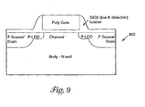
- Fig. 9 depicts an exemplary P channel MOSFET structure 802 with all the components relevant to the parasitic capacitances C gd , C j shown.
- the wordline drive transistors should be fabricated so that lightly doped drain (LDD) regions are present as shown in Fig. 9 so as to minimize parasitic capacitance.
- LDD lightly doped drain
- a low k dielectric SiO2 gate spacer may be added to reduce parasitic capacitance.
- Other techniques may likewise be applied to reduce parasitic capacitance as would be familiar to those of ordinary skill in the art.
- memory devices can be designed to comply with a fixed specified erase time and retention performance.
- a new kind of memory can be designed in which the respective durations of source erase and channel erase can be made adjustable by way of algorithm codes stored in a special function register or other nonvolatile memory dedicated to such control parameters. In this way, the manufacturer can build a generic memory part and then adjust the duration for either erase mechanism at the time of manufacturing test, or else let the user make such adjustment before or after the device has been assembled in the system for the end use.
- a method and apparatus for erasing flash memory includes supplying a negative voltage pulse to the control gate of a memory cell for an erase period, supplying a positive voltage pulse to the source of the memory cell for a period that is shorter in duration than the erase period; and discharging the positive voltage pulse at the end of the second period wherein discharging the positive voltage pulse at the end of the second period effectively increases the magnitude of the negative voltage pulse.
Landscapes
- Non-Volatile Memory (AREA)
- Semiconductor Memories (AREA)
- Read Only Memory (AREA)
- Techniques For Improving Reliability Of Storages (AREA)
Applications Claiming Priority (3)
| Application Number | Priority Date | Filing Date | Title |
|---|---|---|---|
| US10/159,885 US6795348B2 (en) | 2002-05-29 | 2002-05-29 | Method and apparatus for erasing flash memory |
| US159885 | 2002-05-29 | ||
| PCT/US2003/016856 WO2003102962A2 (en) | 2002-05-29 | 2003-05-29 | Method and apparatus for erasing flash memory |
Publications (2)
| Publication Number | Publication Date |
|---|---|
| EP1552529A2 EP1552529A2 (en) | 2005-07-13 |
| EP1552529B1 true EP1552529B1 (en) | 2010-11-03 |
Family
ID=29583053
Family Applications (1)
| Application Number | Title | Priority Date | Filing Date |
|---|---|---|---|
| EP03756241A Expired - Lifetime EP1552529B1 (en) | 2002-05-29 | 2003-05-29 | Method and apparatus for erasing flash memory |
Country Status (10)
| Country | Link |
|---|---|
| US (15) | US6795348B2 (enExample) |
| EP (1) | EP1552529B1 (enExample) |
| JP (1) | JP4359560B2 (enExample) |
| KR (1) | KR100650088B1 (enExample) |
| CN (1) | CN100495574C (enExample) |
| AT (1) | ATE487219T1 (enExample) |
| AU (1) | AU2003247433A1 (enExample) |
| DE (1) | DE60334828D1 (enExample) |
| SG (1) | SG152042A1 (enExample) |
| WO (1) | WO2003102962A2 (enExample) |
Cited By (1)
| Publication number | Priority date | Publication date | Assignee | Title |
|---|---|---|---|---|
| US11251189B2 (en) | 2009-02-09 | 2022-02-15 | Longitude Flash Memory Solutions Ltd. | Gate fringing effect based channel formation for semiconductor device |
Families Citing this family (39)
| Publication number | Priority date | Publication date | Assignee | Title |
|---|---|---|---|---|
| US6795348B2 (en) * | 2002-05-29 | 2004-09-21 | Micron Technology, Inc. | Method and apparatus for erasing flash memory |
| US6862216B1 (en) * | 2004-06-29 | 2005-03-01 | National Semiconductor Corporation | Non-volatile memory cell with gated diode and MOS transistor and method for using such cell |
| US7468299B2 (en) * | 2005-08-04 | 2008-12-23 | Macronix International Co., Ltd. | Non-volatile memory cells and methods of manufacturing the same |
| US7236404B2 (en) * | 2005-08-24 | 2007-06-26 | Macronix International Co. Ltd. | Structures and methods for enhancing erase uniformity in an NROM array |
| US20070047327A1 (en) * | 2005-08-31 | 2007-03-01 | Micron Technology, Inc. | Erase method for flash memory |
| US7567458B2 (en) * | 2005-09-26 | 2009-07-28 | Silicon Storage Technology, Inc. | Flash memory array having control/decode circuitry for disabling top gates of defective memory cells |
| US7151712B1 (en) * | 2005-10-19 | 2006-12-19 | Winbond Electronics Corp. | Row decoder with low gate induce drain leakage current |
| KR100704021B1 (ko) * | 2005-11-08 | 2007-04-04 | 삼성전자주식회사 | 신뢰성을 향상시키는 불휘발성 반도체 메모리 장치의데이터 소거방법 |
| US7483311B2 (en) * | 2006-02-07 | 2009-01-27 | Micron Technology, Inc. | Erase operation in a flash memory device |
| US7277357B1 (en) * | 2006-06-05 | 2007-10-02 | Micron Technology, Inc. | Method and apparatus for reducing oscillation in synchronous circuits |
| KR100842401B1 (ko) * | 2006-10-18 | 2008-07-01 | 삼성전자주식회사 | 비휘발성 메모리 소자 및 그 제조 방법 |
| US7649783B2 (en) * | 2007-01-25 | 2010-01-19 | Micron Technology, Inc. | Delayed activation of selected wordlines in memory |
| US7778086B2 (en) * | 2007-01-25 | 2010-08-17 | Micron Technology, Inc. | Erase operation control sequencing apparatus, systems, and methods |
| US7656740B2 (en) * | 2007-02-05 | 2010-02-02 | Micron Technology, Inc. | Wordline voltage transfer apparatus, systems, and methods |
| KR101348173B1 (ko) * | 2007-05-25 | 2014-01-08 | 삼성전자주식회사 | 플래시 메모리 장치, 그것의 소거 및 프로그램 방법들,그리고 그것을 포함한 메모리 시스템 |
| US7701780B2 (en) * | 2007-05-31 | 2010-04-20 | Micron Technology, Inc. | Non-volatile memory cell healing |
| US7619931B2 (en) * | 2007-06-26 | 2009-11-17 | Micron Technology, Inc. | Program-verify method with different read and verify pass-through voltages |
| US20090003065A1 (en) * | 2007-06-26 | 2009-01-01 | Micron Technology, Inc. | Flash cell with improved program disturb |
| US7916543B2 (en) * | 2007-10-22 | 2011-03-29 | Micron Technology, Inc. | Memory cell operation |
| US7916544B2 (en) | 2008-01-25 | 2011-03-29 | Micron Technology, Inc. | Random telegraph signal noise reduction scheme for semiconductor memories |
| US7924623B2 (en) | 2008-05-27 | 2011-04-12 | Micron Technology, Inc. | Method for memory cell erasure with a programming monitor of reference cells |
| US7995384B2 (en) | 2008-08-15 | 2011-08-09 | Macronix International Co., Ltd. | Electrically isolated gated diode nonvolatile memory |
| KR101478554B1 (ko) * | 2008-10-02 | 2015-01-06 | 삼성전자 주식회사 | 오버 슈트 전압의 산출 방법 및 그를 이용한 게이트 절연막열화분석방법 |
| US8169833B2 (en) * | 2009-10-01 | 2012-05-01 | Micron Technology, Inc. | Partitioning process to improve memory cell retention |
| CN102034539A (zh) * | 2010-10-25 | 2011-04-27 | 上海宏力半导体制造有限公司 | 纳米晶体器件编程/擦除的方法 |
| US8553463B1 (en) | 2011-03-21 | 2013-10-08 | Lattice Semiconductor Corporation | Voltage discharge circuit having divided discharge current |
| US8829588B2 (en) * | 2011-07-26 | 2014-09-09 | Synopsys, Inc. | NVM bitcell with a replacement control gate and additional floating gate |
| US8743628B2 (en) | 2011-08-08 | 2014-06-03 | Micron Technology, Inc. | Line driver circuits, methods, and apparatuses |
| US9134602B2 (en) | 2013-07-29 | 2015-09-15 | Taiwan Semiconductor Manufacturing Co., Ltd. | Method of manufacturing an extreme ultraviolet (EUV) mask and the mask manufactured therefrom |
| US10034578B2 (en) | 2014-08-21 | 2018-07-31 | W.C. Bradley Co. | High performance electric grill, method, and heat radiating module |
| US9728278B2 (en) | 2014-10-24 | 2017-08-08 | Micron Technology, Inc. | Threshold voltage margin analysis |
| US9349447B1 (en) * | 2015-03-02 | 2016-05-24 | HGST, Inc. | Controlling coupling in large cross-point memory arrays |
| US10453535B2 (en) * | 2015-10-26 | 2019-10-22 | Intel Corporation | Segmented erase in memory |
| US10680006B2 (en) * | 2017-08-11 | 2020-06-09 | Micron Technology, Inc. | Charge trap structure with barrier to blocking region |
| US10446572B2 (en) | 2017-08-11 | 2019-10-15 | Micron Technology, Inc. | Void formation for charge trap structures |
| US10164009B1 (en) | 2017-08-11 | 2018-12-25 | Micron Technology, Inc. | Memory device including voids between control gates |
| US10796729B2 (en) | 2019-02-05 | 2020-10-06 | Micron Technology, Inc. | Dynamic allocation of a capacitive component in a memory device |
| US11194726B2 (en) | 2019-02-25 | 2021-12-07 | Micron Technology, Inc. | Stacked memory dice for combined access operations |
| KR102680867B1 (ko) | 2019-09-03 | 2024-07-04 | 삼성전자주식회사 | 반도체 장치 및 이의 동작 방법 |
Family Cites Families (88)
| Publication number | Priority date | Publication date | Assignee | Title |
|---|---|---|---|---|
| US2991195A (en) * | 1960-02-11 | 1961-07-04 | Lockheed Aircraft Corp | Method of metallizing holes and cavities with a refractory metal |
| US4016588A (en) * | 1974-12-27 | 1977-04-05 | Nippon Electric Company, Ltd. | Non-volatile semiconductor memory device |
| US4384349A (en) * | 1979-10-01 | 1983-05-17 | Texas Instruments Incorporated | High density electrically erasable floating gate dual-injection programmable memory device |
| US4503524A (en) * | 1980-06-02 | 1985-03-05 | Texas Instruments Incorporated | Electrically erasable dual-injector floating gate programmable memory device |
| US4384356A (en) * | 1981-04-03 | 1983-05-17 | Britsol Babcock Inc. | Wide band modem for high speed data transmission |
| JPS644077A (en) * | 1987-06-25 | 1989-01-09 | Mitsubishi Electric Corp | Memory cell |
| US5268319A (en) * | 1988-06-08 | 1993-12-07 | Eliyahou Harari | Highly compact EPROM and flash EEPROM devices |
| US5844842A (en) * | 1989-02-06 | 1998-12-01 | Hitachi, Ltd. | Nonvolatile semiconductor memory device |
| US5077691A (en) * | 1989-10-23 | 1991-12-31 | Advanced Micro Devices, Inc. | Flash EEPROM array with negative gate voltage erase operation |
| JP3204666B2 (ja) * | 1990-11-21 | 2001-09-04 | 株式会社東芝 | 不揮発性半導体記憶装置 |
| US5265059A (en) * | 1991-05-10 | 1993-11-23 | Intel Corporation | Circuitry and method for discharging a drain of a cell of a non-volatile semiconductor memory |
| JPH05102438A (ja) * | 1991-10-04 | 1993-04-23 | Mitsubishi Electric Corp | 不揮発性半導体記憶装置 |
| JPH06103798A (ja) * | 1992-09-18 | 1994-04-15 | Fujitsu Ltd | 半導体記憶装置 |
| US5544103A (en) * | 1992-03-03 | 1996-08-06 | Xicor, Inc. | Compact page-erasable eeprom non-volatile memory |
| DE4311358C2 (de) * | 1992-04-07 | 1999-07-22 | Mitsubishi Electric Corp | Nicht-flüchtige Halbleiterspeichereinrichtung und Betriebsverfahren für eine nicht-flüchtige Halbleiterspeichereinrichtung und Verfahren zum Programmieren von Information in eine nicht-flüchtige Halbleiterspeichereinrichtung |
| EP0596198B1 (en) * | 1992-07-10 | 2000-03-29 | Sony Corporation | Flash eprom with erase verification and address scrambling architecture |
| US5357463A (en) * | 1992-11-17 | 1994-10-18 | Micron Semiconductor, Inc. | Method for reverse programming of a flash EEPROM |
| US5399928A (en) * | 1993-05-28 | 1995-03-21 | Macronix International Co., Ltd. | Negative voltage generator for flash EPROM design |
| US5420798A (en) * | 1993-09-30 | 1995-05-30 | Macronix International Co., Ltd. | Supply voltage detection circuit |
| US5477499A (en) * | 1993-10-13 | 1995-12-19 | Advanced Micro Devices, Inc. | Memory architecture for a three volt flash EEPROM |
| KR970003845B1 (ko) * | 1993-10-28 | 1997-03-22 | 금성일렉트론 주식회사 | 이이피롬 프래쉬 메모리 셀, 메모리 디바이스 및 그 제조방법 |
| US5521867A (en) * | 1993-12-01 | 1996-05-28 | Advanced Micro Devices, Inc. | Adjustable threshold voltage conversion circuit |
| WO1995024057A2 (en) * | 1994-03-03 | 1995-09-08 | Rohm Corporation | Low voltage one transistor flash eeprom cell using fowler-nordheim programming and erase |
| FR2718289B1 (fr) * | 1994-03-30 | 1996-08-02 | Sgs Thomson Microelectronics | Cellule mémoire électriquement programmable. |
| EP0690452A3 (en) * | 1994-06-28 | 1999-01-07 | Advanced Micro Devices, Inc. | Electrically erasable memory and method of erasure |
| JPH08148580A (ja) * | 1994-08-01 | 1996-06-07 | Seiko Instr Inc | 半導体集積回路装置 |
| US5485423A (en) * | 1994-10-11 | 1996-01-16 | Advanced Micro Devices, Inc. | Method for eliminating of cycling-induced electron trapping in the tunneling oxide of 5 volt only flash EEPROMS |
| US5808937A (en) * | 1994-12-16 | 1998-09-15 | National Semiconductor Corporation | Self-convergent method for programming FLASH and EEPROM memory cells that moves the threshold voltage from an erased threshold voltage range to one of a plurality of programmed threshold voltage ranges |
| US5491657A (en) * | 1995-02-24 | 1996-02-13 | Advanced Micro Devices, Inc. | Method for bulk (or byte) charging and discharging an array of flash EEPROM memory cells |
| US5617357A (en) * | 1995-04-07 | 1997-04-01 | Advanced Micro Devices, Inc. | Flash EEPROM memory with improved discharge speed using substrate bias and method therefor |
| US5650964A (en) * | 1995-06-07 | 1997-07-22 | Advanced Micro Devices, Inc. | Method of inhibiting degradation of ultra short channel charge-carrying devices during discharge |
| JP3878681B2 (ja) * | 1995-06-15 | 2007-02-07 | 株式会社ルネサステクノロジ | 不揮発性半導体記憶装置 |
| CN1187907A (zh) * | 1995-07-17 | 1998-07-15 | 西门子公司 | 电可擦除可编程的、非易失的存储单元 |
| US5576992A (en) * | 1995-08-30 | 1996-11-19 | Texas Instruments Incorporated | Extended-life method for soft-programming floating-gate memory cells |
| US5781477A (en) * | 1996-02-23 | 1998-07-14 | Micron Quantum Devices, Inc. | Flash memory system having fast erase operation |
| JP2833585B2 (ja) * | 1996-05-17 | 1998-12-09 | 日本電気株式会社 | 半導体不揮発性記憶装置 |
| KR100192584B1 (ko) * | 1996-06-05 | 1999-06-15 | 윤종용 | 불휘발성 반도체 메모리 장치의 소거 방법 |
| US6381670B1 (en) * | 1997-01-07 | 2002-04-30 | Aplus Flash Technology, Inc. | Flash memory array having maximum and minimum threshold voltage detection for eliminating over-erasure problem and enhancing write operation |
| JPH1055689A (ja) * | 1996-08-13 | 1998-02-24 | Denso Corp | フラッシュメモリの消去方法 |
| JPH1083689A (ja) * | 1996-09-10 | 1998-03-31 | Mitsubishi Electric Corp | 不揮発性半導体記憶装置 |
| US5852306A (en) * | 1997-01-29 | 1998-12-22 | Micron Technology, Inc. | Flash memory with nanocrystalline silicon film floating gate |
| DE19880311B3 (de) * | 1997-02-12 | 2017-06-22 | Hyundai Electronics America Inc. | Nichtflüchtige Speicherstruktur |
| US5978276A (en) * | 1997-04-11 | 1999-11-02 | Programmable Silicon Solutions | Electrically erasable nonvolatile memory |
| US6097632A (en) * | 1997-04-18 | 2000-08-01 | Micron Technology, Inc. | Source regulation circuit for an erase operation of flash memory |
| US5726933A (en) * | 1997-05-15 | 1998-03-10 | Taiwan Semiconductor Manufacturing Company, Ltd. | Clipped sine shaped waveform to reduce the cycling-induced electron trapping in the tunneling oxide of flash EEPROM |
| JP3171235B2 (ja) * | 1997-05-29 | 2001-05-28 | 日本電気株式会社 | 不揮発性半導体メモリ |
| US5862078A (en) * | 1997-08-11 | 1999-01-19 | Taiwan Semiconductor Manufacturing Company, Ltd. | Mixed mode erase method to improve flash eeprom write/erase threshold closure |
| TW406423B (en) * | 1997-08-30 | 2000-09-21 | Hyundai Electronics Ind | Flash memory device |
| US5838618A (en) * | 1997-09-11 | 1998-11-17 | Taiwan Semiconductor Manufacturing Company Ltd. | Bi-modal erase method for eliminating cycling-induced flash EEPROM cell write/erase threshold closure |
| US5949717A (en) * | 1997-09-12 | 1999-09-07 | Taiwan Semiconductor Manufacturing Company, Ltd. | Method to improve flash EEPROM cell write/erase threshold voltage closure |
| US5903499A (en) * | 1997-09-12 | 1999-05-11 | Taiwan Semiconductor Manufacturing Company, Ltd. | Method to erase a flash EEPROM using negative gate source erase followed by a high negative gate erase |
| US5828605A (en) * | 1997-10-14 | 1998-10-27 | Taiwan Semiconductor Manufacturing Company Ltd. | Snapback reduces the electron and hole trapping in the tunneling oxide of flash EEPROM |
| US6055183A (en) * | 1997-10-24 | 2000-04-25 | Taiwan Semiconductor Manufacturing Company, Ltd. | Erase method of flash EEPROM by using snapback characteristic |
| KR100481841B1 (ko) * | 1997-11-25 | 2005-08-25 | 삼성전자주식회사 | 음의고전압을방전시키기위한회로를구비한플래시메모리장치 |
| US6026026A (en) * | 1997-12-05 | 2000-02-15 | Hyundai Electronics America, Inc. | Self-convergence of post-erase threshold voltages in a flash memory cell using transient response |
| US6243299B1 (en) * | 1998-02-27 | 2001-06-05 | Micron Technology, Inc. | Flash memory system having fast erase operation |
| FR2776820B1 (fr) * | 1998-03-24 | 2000-05-26 | Sgs Thomson Microelectronics | Memoire a grille flottante electriquement effacable organisee en mots |
| US6055184A (en) * | 1998-09-02 | 2000-04-25 | Texas Instruments Incorporated | Semiconductor memory device having programmable parallel erase operation |
| US6049484A (en) * | 1998-09-10 | 2000-04-11 | Taiwan Semiconductor Manufacturing Company | Erase method to improve flash EEPROM endurance by combining high voltage source erase and negative gate erase |
| US6064595A (en) * | 1998-12-23 | 2000-05-16 | Vantis Corporation | Floating gate memory apparatus and method for selected programming thereof |
| KR100301506B1 (ko) * | 1998-12-28 | 2001-11-30 | 구자홍 | 리니어압축기의오일공급장치 |
| US6049486A (en) * | 1999-01-04 | 2000-04-11 | Taiwan Semiconductor Manufacturing Company | Triple mode erase scheme for improving flash EEPROM cell threshold voltage (VT) cycling closure effect |
| JP3613072B2 (ja) * | 1999-06-02 | 2005-01-26 | 株式会社デンソー | 不揮発性半導体メモリの電荷保持寿命評価方法 |
| JP3694422B2 (ja) * | 1999-06-21 | 2005-09-14 | シャープ株式会社 | ロウデコーダ回路 |
| US6172914B1 (en) * | 1999-08-13 | 2001-01-09 | Advanced Micro Devices, Inc. | Concurrent erase verify scheme for flash memory applications |
| US6236608B1 (en) | 1999-08-16 | 2001-05-22 | Alliance Semiconductor | Technique to improve the source leakage of flash EPROM cells during source erase |
| US6243298B1 (en) * | 1999-08-19 | 2001-06-05 | Azalea Microelectronics Corporation | Non-volatile memory cell capable of being programmed and erased through substantially separate areas of one of its drain-side and source-side regions |
| US6122201A (en) * | 1999-10-20 | 2000-09-19 | Taiwan Semiconductor Manufacturing Company | Clipped sine wave channel erase method to reduce oxide trapping charge generation rate of flash EEPROM |
| KR100319558B1 (ko) * | 1999-11-01 | 2002-01-05 | 윤종용 | 읽기 시간을 줄일 수 있는 불휘발성 반도체 메모리 장치 |
| US6285588B1 (en) * | 1999-12-01 | 2001-09-04 | Advanced Micro Devices, Inc. | Erase scheme to tighten the threshold voltage distribution of EEPROM flash memory cells |
| US6160740A (en) * | 1999-12-17 | 2000-12-12 | Advanced Micro Devices, Inc. | Method to provide a reduced constant E-field during erase of EEPROMs for reliability improvement |
| US6518122B1 (en) * | 1999-12-17 | 2003-02-11 | Chartered Semiconductor Manufacturing Ltd. | Low voltage programmable and erasable flash EEPROM |
| US6485588B1 (en) * | 2000-01-20 | 2002-11-26 | Trw Inc. | Autoignition material additive |
| US6563741B2 (en) * | 2001-01-30 | 2003-05-13 | Micron Technology, Inc. | Flash memory device and method of erasing |
| US6456533B1 (en) * | 2001-02-28 | 2002-09-24 | Advanced Micro Devices, Inc. | Higher program VT and faster programming rates based on improved erase methods |
| US6671208B2 (en) * | 2001-07-27 | 2003-12-30 | Sharp Kabushiki Kaisha | Nonvolatile semiconductor storage device with limited consumption current during erasure and erase method therefor |
| JP3648185B2 (ja) * | 2001-09-13 | 2005-05-18 | マクロニクス インターナショナル カンパニイ リミテッド | フラッシュ・イーピーロム集積回路におけるデータ・パターンをプログラムする方法 |
| US6515909B1 (en) * | 2001-10-05 | 2003-02-04 | Micron Technology Inc. | Flash memory device with a variable erase pulse |
| JP2004072060A (ja) * | 2001-11-22 | 2004-03-04 | Innotech Corp | トランジスタとそれを用いた半導体メモリ、およびトランジスタの駆動方法 |
| US6714458B2 (en) * | 2002-02-11 | 2004-03-30 | Micron Technology, Inc. | High voltage positive and negative two-phase discharge system and method for channel erase in flash memory devices |
| US6784480B2 (en) * | 2002-02-12 | 2004-08-31 | Micron Technology, Inc. | Asymmetric band-gap engineered nonvolatile memory device |
| US6614693B1 (en) * | 2002-03-19 | 2003-09-02 | Taiwan Semiconductor Manufacturing Company | Combination erase waveform to reduce oxide trapping centers generation rate of flash EEPROM |
| US6795348B2 (en) * | 2002-05-29 | 2004-09-21 | Micron Technology, Inc. | Method and apparatus for erasing flash memory |
| US6894931B2 (en) * | 2002-06-20 | 2005-05-17 | Kabushiki Kaisha Toshiba | Nonvolatile semiconductor memory device |
| KR20040008526A (ko) * | 2002-07-18 | 2004-01-31 | 주식회사 하이닉스반도체 | 플래시 메모리 셀의 소거 방법 |
| JP4086583B2 (ja) * | 2002-08-08 | 2008-05-14 | シャープ株式会社 | 不揮発性半導体メモリ装置およびデータ書き込み制御方法 |
| US6829166B2 (en) * | 2002-09-13 | 2004-12-07 | Ememory Technology Inc. | Method for controlling a non-volatile dynamic random access memory |
| US6903407B1 (en) * | 2003-10-14 | 2005-06-07 | Advanced Micro Devices, Inc. | Non volatile charge trapping dielectric memory cell structure with gate hole injection erase |
-
2002
- 2002-05-29 US US10/159,885 patent/US6795348B2/en not_active Expired - Lifetime
-
2003
- 2003-05-29 CN CNB038184400A patent/CN100495574C/zh not_active Expired - Fee Related
- 2003-05-29 SG SG200500538-4A patent/SG152042A1/en unknown
- 2003-05-29 WO PCT/US2003/016856 patent/WO2003102962A2/en not_active Ceased
- 2003-05-29 EP EP03756241A patent/EP1552529B1/en not_active Expired - Lifetime
- 2003-05-29 AT AT03756241T patent/ATE487219T1/de not_active IP Right Cessation
- 2003-05-29 KR KR1020047019353A patent/KR100650088B1/ko not_active Expired - Fee Related
- 2003-05-29 DE DE60334828T patent/DE60334828D1/de not_active Expired - Lifetime
- 2003-05-29 JP JP2004509958A patent/JP4359560B2/ja not_active Expired - Fee Related
- 2003-05-29 AU AU2003247433A patent/AU2003247433A1/en not_active Abandoned
-
2004
- 2004-06-24 US US10/875,453 patent/US7046557B2/en not_active Expired - Lifetime
- 2004-06-24 US US10/875,452 patent/US7215572B2/en not_active Expired - Lifetime
- 2004-06-24 US US10/876,184 patent/US7099220B2/en not_active Expired - Lifetime
-
2005
- 2005-08-31 US US11/215,963 patent/US7203098B2/en not_active Expired - Lifetime
- 2005-08-31 US US11/216,956 patent/US7277327B2/en not_active Expired - Lifetime
- 2005-08-31 US US11/215,969 patent/US7277326B2/en not_active Expired - Lifetime
- 2005-09-01 US US11/217,813 patent/US7099195B2/en not_active Expired - Lifetime
- 2005-09-01 US US11/217,952 patent/US7280395B2/en not_active Expired - Lifetime
- 2005-09-01 US US11/219,020 patent/US7259996B2/en not_active Expired - Lifetime
- 2005-09-01 US US11/218,855 patent/US7057932B2/en not_active Expired - Fee Related
- 2005-09-01 US US11/217,828 patent/US7277328B2/en not_active Expired - Lifetime
- 2005-09-01 US US11/217,825 patent/US7068543B2/en not_active Expired - Fee Related
- 2005-09-01 US US11/217,920 patent/US7272044B2/en not_active Expired - Lifetime
- 2005-09-01 US US11/217,820 patent/US7200048B2/en not_active Expired - Lifetime
Cited By (2)
| Publication number | Priority date | Publication date | Assignee | Title |
|---|---|---|---|---|
| US11251189B2 (en) | 2009-02-09 | 2022-02-15 | Longitude Flash Memory Solutions Ltd. | Gate fringing effect based channel formation for semiconductor device |
| US11950412B2 (en) | 2009-02-09 | 2024-04-02 | Longitude Flash Memory Solutions Ltd. | Gate fringing effect based channel formation for semiconductor device |
Also Published As
Similar Documents
| Publication | Publication Date | Title |
|---|---|---|
| EP1552529B1 (en) | Method and apparatus for erasing flash memory | |
| EP1204978A1 (en) | Soft programming method for memory cells to tighten the vt distribution using a ramped gate voltage | |
| JP3811760B2 (ja) | フラッシュメモリ用途のための傾斜付きまたは段階的ゲートチャネル消去 | |
| US20040062118A1 (en) | Erase of a non-volatile memory | |
| JP4641697B2 (ja) | 信頼性の改善のためにeepromの消去中に減じられた一定の電界を提供するための方法 | |
| US6160740A (en) | Method to provide a reduced constant E-field during erase of EEPROMs for reliability improvement |
Legal Events
| Date | Code | Title | Description |
|---|---|---|---|
| PUAI | Public reference made under article 153(3) epc to a published international application that has entered the european phase |
Free format text: ORIGINAL CODE: 0009012 |
|
| 17P | Request for examination filed |
Effective date: 20041221 |
|
| AK | Designated contracting states |
Kind code of ref document: A2 Designated state(s): AT BE BG CH CY CZ DE DK EE ES FI FR GB GR HU IE IT LI LU MC NL PT RO SE SI SK TR |
|
| AX | Request for extension of the european patent |
Extension state: AL LT LV MK |
|
| 17Q | First examination report despatched |
Effective date: 20070302 |
|
| GRAP | Despatch of communication of intention to grant a patent |
Free format text: ORIGINAL CODE: EPIDOSNIGR1 |
|
| GRAS | Grant fee paid |
Free format text: ORIGINAL CODE: EPIDOSNIGR3 |
|
| GRAA | (expected) grant |
Free format text: ORIGINAL CODE: 0009210 |
|
| AK | Designated contracting states |
Kind code of ref document: B1 Designated state(s): AT BE BG CH CY CZ DE DK EE ES FI FR GB GR HU IE IT LI LU MC NL PT RO SE SI SK TR |
|
| AX | Request for extension of the european patent |
Extension state: AL LT LV MK |
|
| REG | Reference to a national code |
Ref country code: GB Ref legal event code: FG4D |
|
| REG | Reference to a national code |
Ref country code: CH Ref legal event code: EP |
|
| REG | Reference to a national code |
Ref country code: IE Ref legal event code: FG4D |
|
| REF | Corresponds to: |
Ref document number: 60334828 Country of ref document: DE Date of ref document: 20101216 Kind code of ref document: P |
|
| REG | Reference to a national code |
Ref country code: NL Ref legal event code: VDEP Effective date: 20101103 |
|
| LTIE | Lt: invalidation of european patent or patent extension |
Effective date: 20101103 |
|
| PG25 | Lapsed in a contracting state [announced via postgrant information from national office to epo] |
Ref country code: AT Free format text: LAPSE BECAUSE OF FAILURE TO SUBMIT A TRANSLATION OF THE DESCRIPTION OR TO PAY THE FEE WITHIN THE PRESCRIBED TIME-LIMIT Effective date: 20101103 Ref country code: PT Free format text: LAPSE BECAUSE OF FAILURE TO SUBMIT A TRANSLATION OF THE DESCRIPTION OR TO PAY THE FEE WITHIN THE PRESCRIBED TIME-LIMIT Effective date: 20110303 Ref country code: SI Free format text: LAPSE BECAUSE OF FAILURE TO SUBMIT A TRANSLATION OF THE DESCRIPTION OR TO PAY THE FEE WITHIN THE PRESCRIBED TIME-LIMIT Effective date: 20101103 Ref country code: FI Free format text: LAPSE BECAUSE OF FAILURE TO SUBMIT A TRANSLATION OF THE DESCRIPTION OR TO PAY THE FEE WITHIN THE PRESCRIBED TIME-LIMIT Effective date: 20101103 Ref country code: SE Free format text: LAPSE BECAUSE OF FAILURE TO SUBMIT A TRANSLATION OF THE DESCRIPTION OR TO PAY THE FEE WITHIN THE PRESCRIBED TIME-LIMIT Effective date: 20101103 Ref country code: NL Free format text: LAPSE BECAUSE OF FAILURE TO SUBMIT A TRANSLATION OF THE DESCRIPTION OR TO PAY THE FEE WITHIN THE PRESCRIBED TIME-LIMIT Effective date: 20101103 Ref country code: BG Free format text: LAPSE BECAUSE OF FAILURE TO SUBMIT A TRANSLATION OF THE DESCRIPTION OR TO PAY THE FEE WITHIN THE PRESCRIBED TIME-LIMIT Effective date: 20110203 |
|
| PG25 | Lapsed in a contracting state [announced via postgrant information from national office to epo] |
Ref country code: GR Free format text: LAPSE BECAUSE OF FAILURE TO SUBMIT A TRANSLATION OF THE DESCRIPTION OR TO PAY THE FEE WITHIN THE PRESCRIBED TIME-LIMIT Effective date: 20110204 |
|
| PG25 | Lapsed in a contracting state [announced via postgrant information from national office to epo] |
Ref country code: ES Free format text: LAPSE BECAUSE OF FAILURE TO SUBMIT A TRANSLATION OF THE DESCRIPTION OR TO PAY THE FEE WITHIN THE PRESCRIBED TIME-LIMIT Effective date: 20110214 Ref country code: BE Free format text: LAPSE BECAUSE OF FAILURE TO SUBMIT A TRANSLATION OF THE DESCRIPTION OR TO PAY THE FEE WITHIN THE PRESCRIBED TIME-LIMIT Effective date: 20101103 Ref country code: CZ Free format text: LAPSE BECAUSE OF FAILURE TO SUBMIT A TRANSLATION OF THE DESCRIPTION OR TO PAY THE FEE WITHIN THE PRESCRIBED TIME-LIMIT Effective date: 20101103 Ref country code: EE Free format text: LAPSE BECAUSE OF FAILURE TO SUBMIT A TRANSLATION OF THE DESCRIPTION OR TO PAY THE FEE WITHIN THE PRESCRIBED TIME-LIMIT Effective date: 20101103 |
|
| PG25 | Lapsed in a contracting state [announced via postgrant information from national office to epo] |
Ref country code: DK Free format text: LAPSE BECAUSE OF FAILURE TO SUBMIT A TRANSLATION OF THE DESCRIPTION OR TO PAY THE FEE WITHIN THE PRESCRIBED TIME-LIMIT Effective date: 20101103 Ref country code: SK Free format text: LAPSE BECAUSE OF FAILURE TO SUBMIT A TRANSLATION OF THE DESCRIPTION OR TO PAY THE FEE WITHIN THE PRESCRIBED TIME-LIMIT Effective date: 20101103 Ref country code: RO Free format text: LAPSE BECAUSE OF FAILURE TO SUBMIT A TRANSLATION OF THE DESCRIPTION OR TO PAY THE FEE WITHIN THE PRESCRIBED TIME-LIMIT Effective date: 20101103 |
|
| PLBE | No opposition filed within time limit |
Free format text: ORIGINAL CODE: 0009261 |
|
| STAA | Information on the status of an ep patent application or granted ep patent |
Free format text: STATUS: NO OPPOSITION FILED WITHIN TIME LIMIT |
|
| 26N | No opposition filed |
Effective date: 20110804 |
|
| REG | Reference to a national code |
Ref country code: DE Ref legal event code: R097 Ref document number: 60334828 Country of ref document: DE Effective date: 20110804 |
|
| PG25 | Lapsed in a contracting state [announced via postgrant information from national office to epo] |
Ref country code: MC Free format text: LAPSE BECAUSE OF NON-PAYMENT OF DUE FEES Effective date: 20110531 Ref country code: IT Free format text: LAPSE BECAUSE OF FAILURE TO SUBMIT A TRANSLATION OF THE DESCRIPTION OR TO PAY THE FEE WITHIN THE PRESCRIBED TIME-LIMIT Effective date: 20101103 |
|
| REG | Reference to a national code |
Ref country code: CH Ref legal event code: PL |
|
| PG25 | Lapsed in a contracting state [announced via postgrant information from national office to epo] |
Ref country code: LI Free format text: LAPSE BECAUSE OF NON-PAYMENT OF DUE FEES Effective date: 20110531 Ref country code: CH Free format text: LAPSE BECAUSE OF NON-PAYMENT OF DUE FEES Effective date: 20110531 |
|
| REG | Reference to a national code |
Ref country code: FR Ref legal event code: ST Effective date: 20120131 |
|
| REG | Reference to a national code |
Ref country code: IE Ref legal event code: MM4A |
|
| REG | Reference to a national code |
Ref country code: DE Ref legal event code: R119 Ref document number: 60334828 Country of ref document: DE Effective date: 20111201 |
|
| PG25 | Lapsed in a contracting state [announced via postgrant information from national office to epo] |
Ref country code: FR Free format text: LAPSE BECAUSE OF NON-PAYMENT OF DUE FEES Effective date: 20110531 Ref country code: IE Free format text: LAPSE BECAUSE OF NON-PAYMENT OF DUE FEES Effective date: 20110529 |
|
| PGFP | Annual fee paid to national office [announced via postgrant information from national office to epo] |
Ref country code: GB Payment date: 20120523 Year of fee payment: 10 |
|
| PG25 | Lapsed in a contracting state [announced via postgrant information from national office to epo] |
Ref country code: CY Free format text: LAPSE BECAUSE OF FAILURE TO SUBMIT A TRANSLATION OF THE DESCRIPTION OR TO PAY THE FEE WITHIN THE PRESCRIBED TIME-LIMIT Effective date: 20101103 Ref country code: LU Free format text: LAPSE BECAUSE OF NON-PAYMENT OF DUE FEES Effective date: 20110529 |
|
| PG25 | Lapsed in a contracting state [announced via postgrant information from national office to epo] |
Ref country code: DE Free format text: LAPSE BECAUSE OF NON-PAYMENT OF DUE FEES Effective date: 20111201 |
|
| PG25 | Lapsed in a contracting state [announced via postgrant information from national office to epo] |
Ref country code: TR Free format text: LAPSE BECAUSE OF FAILURE TO SUBMIT A TRANSLATION OF THE DESCRIPTION OR TO PAY THE FEE WITHIN THE PRESCRIBED TIME-LIMIT Effective date: 20101103 |
|
| PG25 | Lapsed in a contracting state [announced via postgrant information from national office to epo] |
Ref country code: HU Free format text: LAPSE BECAUSE OF FAILURE TO SUBMIT A TRANSLATION OF THE DESCRIPTION OR TO PAY THE FEE WITHIN THE PRESCRIBED TIME-LIMIT Effective date: 20101103 |
|
| GBPC | Gb: european patent ceased through non-payment of renewal fee |
Effective date: 20130529 |
|
| PG25 | Lapsed in a contracting state [announced via postgrant information from national office to epo] |
Ref country code: GB Free format text: LAPSE BECAUSE OF NON-PAYMENT OF DUE FEES Effective date: 20130529 |