US6160740A - Method to provide a reduced constant E-field during erase of EEPROMs for reliability improvement - Google Patents
Method to provide a reduced constant E-field during erase of EEPROMs for reliability improvement Download PDFInfo
- Publication number
- US6160740A US6160740A US09/490,351 US49035100A US6160740A US 6160740 A US6160740 A US 6160740A US 49035100 A US49035100 A US 49035100A US 6160740 A US6160740 A US 6160740A
- Authority
- US
- United States
- Prior art keywords
- gate
- erase
- source
- voltage
- cell
- Prior art date
- Legal status (The legal status is an assumption and is not a legal conclusion. Google has not performed a legal analysis and makes no representation as to the accuracy of the status listed.)
- Expired - Lifetime
Links
- 238000000034 method Methods 0.000 title claims abstract description 49
- 230000002829 reductive effect Effects 0.000 title description 8
- 230000005684 electric field Effects 0.000 claims abstract description 28
- 108091006146 Channels Proteins 0.000 description 17
- 239000000758 substrate Substances 0.000 description 9
- 238000010586 diagram Methods 0.000 description 8
- 239000004065 semiconductor Substances 0.000 description 6
- 230000005641 tunneling Effects 0.000 description 6
- 230000007423 decrease Effects 0.000 description 5
- 239000002784 hot electron Substances 0.000 description 5
- 239000013642 negative control Substances 0.000 description 5
- 230000008878 coupling Effects 0.000 description 4
- 238000010168 coupling process Methods 0.000 description 4
- 238000005859 coupling reaction Methods 0.000 description 4
- 238000004377 microelectronic Methods 0.000 description 4
- 238000012986 modification Methods 0.000 description 4
- 230000004048 modification Effects 0.000 description 4
- 230000002441 reversible effect Effects 0.000 description 4
- 230000005689 Fowler Nordheim tunneling Effects 0.000 description 3
- 230000008901 benefit Effects 0.000 description 3
- 230000015556 catabolic process Effects 0.000 description 3
- 238000006731 degradation reaction Methods 0.000 description 3
- 108010075750 P-Type Calcium Channels Proteins 0.000 description 2
- VYPSYNLAJGMNEJ-UHFFFAOYSA-N Silicium dioxide Chemical compound O=[Si]=O VYPSYNLAJGMNEJ-UHFFFAOYSA-N 0.000 description 2
- 230000002411 adverse Effects 0.000 description 2
- 239000000969 carrier Substances 0.000 description 2
- 238000012512 characterization method Methods 0.000 description 2
- 238000010276 construction Methods 0.000 description 2
- 230000005669 field effect Effects 0.000 description 2
- 238000002347 injection Methods 0.000 description 2
- 239000007924 injection Substances 0.000 description 2
- 239000012212 insulator Substances 0.000 description 2
- LZIAMMQBHJIZAG-UHFFFAOYSA-N 2-[di(propan-2-yl)amino]ethyl carbamimidothioate Chemical compound CC(C)N(C(C)C)CCSC(N)=N LZIAMMQBHJIZAG-UHFFFAOYSA-N 0.000 description 1
- 230000015572 biosynthetic process Effects 0.000 description 1
- 238000005094 computer simulation Methods 0.000 description 1
- 230000003247 decreasing effect Effects 0.000 description 1
- 230000001419 dependent effect Effects 0.000 description 1
- 230000005527 interface trap Effects 0.000 description 1
- 230000000670 limiting effect Effects 0.000 description 1
- 239000011159 matrix material Substances 0.000 description 1
- 235000012239 silicon dioxide Nutrition 0.000 description 1
- 239000000377 silicon dioxide Substances 0.000 description 1
- 239000000243 solution Substances 0.000 description 1
Images


Classifications
-
- G—PHYSICS
- G11—INFORMATION STORAGE
- G11C—STATIC STORES
- G11C16/00—Erasable programmable read-only memories
- G11C16/02—Erasable programmable read-only memories electrically programmable
- G11C16/06—Auxiliary circuits, e.g. for writing into memory
- G11C16/10—Programming or data input circuits
- G11C16/14—Circuits for erasing electrically, e.g. erase voltage switching circuits
Abstract
Description
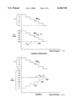
E.sub.field ˜a.sub.g (V.sub.gate -V.sub.th +V.sub.tuv)+(a.sub.s -1)V.sub.source (1)
E.sub.field ˜a.sub.g (V.sub.gate -V.sub.th +V.sub.tuv)+(a.sub.s -1)V.sub.source (1)
Claims (3)
Priority Applications (6)
| Application Number | Priority Date | Filing Date | Title |
|---|---|---|---|
| US09/490,351 US6160740A (en) | 1999-12-17 | 2000-01-24 | Method to provide a reduced constant E-field during erase of EEPROMs for reliability improvement |
| PCT/US2000/033044 WO2001045113A1 (en) | 1999-12-17 | 2000-12-05 | Method to provide a reduced constant e-field during erase of eeproms for reliability improvement |
| EP00983940A EP1256117A1 (en) | 1999-12-17 | 2000-12-05 | Method to provide a reduced constant e-field during erase of eeproms for reliability improvement |
| KR1020027007781A KR100655944B1 (en) | 1999-12-17 | 2000-12-05 | Method to provide a reduced constant e-field during erase of eeproms for reliability iprovement |
| JP2001545318A JP4641697B2 (en) | 1999-12-17 | 2000-12-05 | Method for providing a constant electric field reduced during erasure of EEPROM for improved reliability |
| CN00817240A CN1411602A (en) | 1999-12-17 | 2000-12-05 | Method to provide reduced constant E-field during erase of EEPROM for reliability improvement |
Applications Claiming Priority (2)
| Application Number | Priority Date | Filing Date | Title |
|---|---|---|---|
| US17232899P | 1999-12-17 | 1999-12-17 | |
| US09/490,351 US6160740A (en) | 1999-12-17 | 2000-01-24 | Method to provide a reduced constant E-field during erase of EEPROMs for reliability improvement |
Publications (1)
| Publication Number | Publication Date |
|---|---|
| US6160740A true US6160740A (en) | 2000-12-12 |
Family
ID=26867975
Family Applications (1)
| Application Number | Title | Priority Date | Filing Date |
|---|---|---|---|
| US09/490,351 Expired - Lifetime US6160740A (en) | 1999-12-17 | 2000-01-24 | Method to provide a reduced constant E-field during erase of EEPROMs for reliability improvement |
Country Status (1)
| Country | Link |
|---|---|
| US (1) | US6160740A (en) |
Cited By (5)
| Publication number | Priority date | Publication date | Assignee | Title |
|---|---|---|---|---|
| US20030210573A1 (en) * | 2002-05-08 | 2003-11-13 | Chang-Hyun Lee | Electrically erasable charge trap nonvolatile memory cells having erase threshold voltage that is higher than an initial threshold voltage, and methods of erasing and designing same |
| US20050141286A1 (en) * | 2003-12-31 | 2005-06-30 | Dongbuanam Semiconductor Inc. | Erase method in flash memory device |
| US20060007743A1 (en) * | 2002-05-29 | 2006-01-12 | Micron Technology, Inc. | Flash memory |
| US20060279999A1 (en) * | 2005-06-13 | 2006-12-14 | Samsung Electronics Co., Ltd. | Methods of Erasing Flash Memory Devices by Applying Wordline Bias Voltages Having Multiple Levels and Related Flash Memory Devices |
| CN105448346A (en) * | 2014-08-22 | 2016-03-30 | 中芯国际集成电路制造(上海)有限公司 | Method for testing reliability of memory cell |
Citations (6)
| Publication number | Priority date | Publication date | Assignee | Title |
|---|---|---|---|---|
| US5077691A (en) * | 1989-10-23 | 1991-12-31 | Advanced Micro Devices, Inc. | Flash EEPROM array with negative gate voltage erase operation |
| US5428578A (en) * | 1993-08-12 | 1995-06-27 | Texas Instruments Incorporated | Biasing circuit and method to achieve compaction and self-limiting erase in flash EEPROMs |
| US5680348A (en) * | 1995-12-01 | 1997-10-21 | Advanced Micro Devices, Inc. | Power supply independent current source for FLASH EPROM erasure |
| US5805502A (en) * | 1995-05-12 | 1998-09-08 | Advanced Micro Devices, Inc. | System for constant field erasure in a FLASH EPROM |
| US5917757A (en) * | 1996-08-01 | 1999-06-29 | Aplus Flash Technology, Inc. | Flash memory with high speed erasing structure using thin oxide semiconductor devices |
| US6049479A (en) * | 1999-09-23 | 2000-04-11 | Advanced Micro Devices, Inc. | Operational approach for the suppression of bi-directional tunnel oxide stress of a flash cell |
-
2000
- 2000-01-24 US US09/490,351 patent/US6160740A/en not_active Expired - Lifetime
Patent Citations (6)
| Publication number | Priority date | Publication date | Assignee | Title |
|---|---|---|---|---|
| US5077691A (en) * | 1989-10-23 | 1991-12-31 | Advanced Micro Devices, Inc. | Flash EEPROM array with negative gate voltage erase operation |
| US5428578A (en) * | 1993-08-12 | 1995-06-27 | Texas Instruments Incorporated | Biasing circuit and method to achieve compaction and self-limiting erase in flash EEPROMs |
| US5805502A (en) * | 1995-05-12 | 1998-09-08 | Advanced Micro Devices, Inc. | System for constant field erasure in a FLASH EPROM |
| US5680348A (en) * | 1995-12-01 | 1997-10-21 | Advanced Micro Devices, Inc. | Power supply independent current source for FLASH EPROM erasure |
| US5917757A (en) * | 1996-08-01 | 1999-06-29 | Aplus Flash Technology, Inc. | Flash memory with high speed erasing structure using thin oxide semiconductor devices |
| US6049479A (en) * | 1999-09-23 | 2000-04-11 | Advanced Micro Devices, Inc. | Operational approach for the suppression of bi-directional tunnel oxide stress of a flash cell |
Cited By (16)
| Publication number | Priority date | Publication date | Assignee | Title |
|---|---|---|---|---|
| US7453736B2 (en) | 2002-05-08 | 2008-11-18 | Samsung Electronics Co., Ltd. | Methods of erasing and designing electrically erasable charge trap nonvolatile memory cells having erase threshold voltage that is higher than an initial threshold voltage |
| US6947330B2 (en) | 2002-05-08 | 2005-09-20 | Samsung Electronics Co., Ltd. | Electrically erasable charge trap nonvolatile memory cells having erase threshold voltage that is higher than an initial threshold voltage |
| US20050237783A1 (en) * | 2002-05-08 | 2005-10-27 | Samsung Electronics Co., Ltd. | Electrically erasable charge trap nonvolatile memory cells having erase threshold voltage that is higher than an initial threshold voltage |
| US20030210573A1 (en) * | 2002-05-08 | 2003-11-13 | Chang-Hyun Lee | Electrically erasable charge trap nonvolatile memory cells having erase threshold voltage that is higher than an initial threshold voltage, and methods of erasing and designing same |
| US7170795B2 (en) | 2002-05-08 | 2007-01-30 | Samsung Electronics Co., Ltd. | Electrically erasable charge trap nonvolatile memory cells having erase threshold voltage that is higher than an initial threshold voltage |
| US20070103990A1 (en) * | 2002-05-08 | 2007-05-10 | Samsung Electronics Co., Ltd. | Methods of erasing and designing electrically erasable charge trap nonvolatile memory cells having erase threshold voltage that is higher than an initial threshold voltage |
| US20060007743A1 (en) * | 2002-05-29 | 2006-01-12 | Micron Technology, Inc. | Flash memory |
| US20060007744A1 (en) * | 2002-05-29 | 2006-01-12 | Micron Technology, Inc. | Flash memory |
| US7057932B2 (en) * | 2002-05-29 | 2006-06-06 | Micron Technology, Inc. | Flash memory |
| US7068543B2 (en) * | 2002-05-29 | 2006-06-27 | Micron Technology, Inc. | Flash memory |
| US20050141286A1 (en) * | 2003-12-31 | 2005-06-30 | Dongbuanam Semiconductor Inc. | Erase method in flash memory device |
| US7161840B2 (en) * | 2003-12-31 | 2007-01-09 | Dongbu Electronics Co., Ltd. | Erase method in flash memory device |
| US20060279999A1 (en) * | 2005-06-13 | 2006-12-14 | Samsung Electronics Co., Ltd. | Methods of Erasing Flash Memory Devices by Applying Wordline Bias Voltages Having Multiple Levels and Related Flash Memory Devices |
| US7397706B2 (en) * | 2005-06-13 | 2008-07-08 | Samsung Electronics Co., Ltd. | Methods of erasing flash memory devices by applying wordline bias voltages having multiple levels and related flash memory devices |
| CN105448346A (en) * | 2014-08-22 | 2016-03-30 | 中芯国际集成电路制造(上海)有限公司 | Method for testing reliability of memory cell |
| CN105448346B (en) * | 2014-08-22 | 2018-09-25 | 中芯国际集成电路制造(上海)有限公司 | The test method of storage unit reliability |
Similar Documents
| Publication | Publication Date | Title |
|---|---|---|
| JP3653186B2 (en) | Nonvolatile memory device programming method | |
| US6172909B1 (en) | Ramped gate technique for soft programming to tighten the Vt distribution | |
| US5416738A (en) | Single transistor flash EPROM cell and method of operation | |
| US6777292B2 (en) | Set of three level concurrent word line bias conditions for a NOR type flash memory array | |
| JP3886673B2 (en) | Nonvolatile semiconductor memory device | |
| US6240016B1 (en) | Method to reduce read gate disturb for flash EEPROM application | |
| EP1175680B1 (en) | Ramped or stepped gate channel erase for flash memory application | |
| JP2007506207A (en) | Boost substrate for flash memory / tab programming | |
| US6466478B1 (en) | Non-volatile semiconductor memory device | |
| US5521867A (en) | Adjustable threshold voltage conversion circuit | |
| US5767729A (en) | Distribution charge pump for nonvolatile memory device | |
| US6469939B1 (en) | Flash memory device with increase of efficiency during an APDE (automatic program disturb after erase) process | |
| US6452840B1 (en) | Feedback method to optimize electric field during channel erase of flash memory devices | |
| US6510085B1 (en) | Method of channel hot electron programming for short channel NOR flash arrays | |
| US6285588B1 (en) | Erase scheme to tighten the threshold voltage distribution of EEPROM flash memory cells | |
| US6141255A (en) | 1 transistor cell for EEPROM application | |
| US6233175B1 (en) | Self-limiting multi-level programming states | |
| KR100655944B1 (en) | Method to provide a reduced constant e-field during erase of eeproms for reliability iprovement | |
| US6160740A (en) | Method to provide a reduced constant E-field during erase of EEPROMs for reliability improvement | |
| US6137727A (en) | Reduction of oxide stress through the use of forward biased body voltage | |
| US6178117B1 (en) | Background correction for charge gain and loss | |
| US6768683B1 (en) | Low column leakage flash memory array | |
| US6147907A (en) | Biasing scheme to reduce stress on non-selected cells during read | |
| TWI489593B (en) | Hot carrier programming of nand flash memory |
Legal Events
| Date | Code | Title | Description |
|---|---|---|---|
| AS | Assignment |
Owner name: ADVANCED MICRO DEVICES, INC., CALIFORNIA Free format text: ASSIGNMENT OF ASSIGNORS INTEREST;ASSIGNOR:CLEVELAND, LEE EDWARD;REEL/FRAME:010545/0310 Effective date: 20000119 |
|
| STCF | Information on status: patent grant |
Free format text: PATENTED CASE |
|
| FPAY | Fee payment |
Year of fee payment: 4 |
|
| AS | Assignment |
Owner name: SPANSION INC., CALIFORNIA Free format text: ASSIGNMENT OF ASSIGNORS INTEREST;ASSIGNOR:ADVANCED MICRO DEVICES, INC.;REEL/FRAME:019028/0656 Effective date: 20070131 |
|
| AS | Assignment |
Owner name: SPANSION LLC, CALIFORNIA Free format text: ASSIGNMENT OF ASSIGNORS INTEREST;ASSIGNOR:SPANSION INC.;REEL/FRAME:019069/0094 Effective date: 20070131 |
|
| FPAY | Fee payment |
Year of fee payment: 8 |
|
| AS | Assignment |
Owner name: BARCLAYS BANK PLC,NEW YORK Free format text: SECURITY AGREEMENT;ASSIGNORS:SPANSION LLC;SPANSION INC.;SPANSION TECHNOLOGY INC.;AND OTHERS;REEL/FRAME:024522/0338 Effective date: 20100510 Owner name: BARCLAYS BANK PLC, NEW YORK Free format text: SECURITY AGREEMENT;ASSIGNORS:SPANSION LLC;SPANSION INC.;SPANSION TECHNOLOGY INC.;AND OTHERS;REEL/FRAME:024522/0338 Effective date: 20100510 |
|
| FPAY | Fee payment |
Year of fee payment: 12 |
|
| AS | Assignment |
Owner name: SPANSION INC., CALIFORNIA Free format text: RELEASE BY SECURED PARTY;ASSIGNOR:BARCLAYS BANK PLC;REEL/FRAME:035201/0159 Effective date: 20150312 Owner name: SPANSION LLC, CALIFORNIA Free format text: RELEASE BY SECURED PARTY;ASSIGNOR:BARCLAYS BANK PLC;REEL/FRAME:035201/0159 Effective date: 20150312 Owner name: SPANSION TECHNOLOGY LLC, CALIFORNIA Free format text: RELEASE BY SECURED PARTY;ASSIGNOR:BARCLAYS BANK PLC;REEL/FRAME:035201/0159 Effective date: 20150312 |
|
| AS | Assignment |
Owner name: MORGAN STANLEY SENIOR FUNDING, INC., NEW YORK Free format text: SECURITY INTEREST;ASSIGNORS:CYPRESS SEMICONDUCTOR CORPORATION;SPANSION LLC;REEL/FRAME:035240/0429 Effective date: 20150312 |
|
| AS | Assignment |
Owner name: CYPRESS SEMICONDUCTOR CORPORATION, CALIFORNIA Free format text: ASSIGNMENT OF ASSIGNORS INTEREST;ASSIGNOR:SPANSION, LLC;REEL/FRAME:036031/0355 Effective date: 20150601 |
|
| AS | Assignment |
Owner name: MONTEREY RESEARCH, LLC, CALIFORNIA Free format text: ASSIGNMENT OF ASSIGNORS INTEREST;ASSIGNOR:CYPRESS SEMICONDUCTOR CORPORATION;REEL/FRAME:040908/0960 Effective date: 20160928 |
|
| AS | Assignment |
Owner name: SPANSION LLC, CALIFORNIA Free format text: RELEASE BY SECURED PARTY;ASSIGNOR:MORGAN STANLEY SENIOR FUNDING, INC.;REEL/FRAME:041175/0939 Effective date: 20160928 Owner name: CYPRESS SEMICONDUCTOR CORPORATION, CALIFORNIA Free format text: RELEASE BY SECURED PARTY;ASSIGNOR:MORGAN STANLEY SENIOR FUNDING, INC.;REEL/FRAME:041175/0939 Effective date: 20160928 |
|
| AS | Assignment |
Owner name: MORGAN STANLEY SENIOR FUNDING, INC., NEW YORK Free format text: CORRECTIVE ASSIGNMENT TO CORRECT THE 8647899 PREVIOUSLY RECORDED ON REEL 035240 FRAME 0429. ASSIGNOR(S) HEREBY CONFIRMS THE SECURITY INTERST;ASSIGNORS:CYPRESS SEMICONDUCTOR CORPORATION;SPANSION LLC;REEL/FRAME:058002/0470 Effective date: 20150312 |