EP1549119A2 - Elektronische Schaltungseinheit und Verfahren zu deren Herstellung - Google Patents
Elektronische Schaltungseinheit und Verfahren zu deren Herstellung Download PDFInfo
- Publication number
- EP1549119A2 EP1549119A2 EP04030634A EP04030634A EP1549119A2 EP 1549119 A2 EP1549119 A2 EP 1549119A2 EP 04030634 A EP04030634 A EP 04030634A EP 04030634 A EP04030634 A EP 04030634A EP 1549119 A2 EP1549119 A2 EP 1549119A2
- Authority
- EP
- European Patent Office
- Prior art keywords
- circuit board
- electronic circuit
- circuit unit
- electrodes
- insulating plate
- Prior art date
- Legal status (The legal status is an assumption and is not a legal conclusion. Google has not performed a legal analysis and makes no representation as to the accuracy of the status listed.)
- Withdrawn
Links
Images

Classifications
-
- H—ELECTRICITY
- H10—SEMICONDUCTOR DEVICES; ELECTRIC SOLID-STATE DEVICES NOT OTHERWISE PROVIDED FOR
- H10W—GENERIC PACKAGES, INTERCONNECTIONS, CONNECTORS OR OTHER CONSTRUCTIONAL DETAILS OF DEVICES COVERED BY CLASS H10
- H10W90/00—Package configurations
-
- H—ELECTRICITY
- H05—ELECTRIC TECHNIQUES NOT OTHERWISE PROVIDED FOR
- H05K—PRINTED CIRCUITS; CASINGS OR CONSTRUCTIONAL DETAILS OF ELECTRIC APPARATUS; MANUFACTURE OF ASSEMBLAGES OF ELECTRICAL COMPONENTS
- H05K1/00—Printed circuits
- H05K1/02—Details
- H05K1/11—Printed elements for providing electric connections to or between printed circuits
- H05K1/111—Pads for surface mounting, e.g. lay-out
- H05K1/112—Pads for surface mounting, e.g. lay-out directly combined with via connections
- H05K1/113—Via provided in pad; Pad over filled via
-
- H—ELECTRICITY
- H05—ELECTRIC TECHNIQUES NOT OTHERWISE PROVIDED FOR
- H05K—PRINTED CIRCUITS; CASINGS OR CONSTRUCTIONAL DETAILS OF ELECTRIC APPARATUS; MANUFACTURE OF ASSEMBLAGES OF ELECTRICAL COMPONENTS
- H05K1/00—Printed circuits
- H05K1/18—Printed circuits structurally associated with non-printed electric components
- H05K1/181—Printed circuits structurally associated with non-printed electric components associated with surface mounted components
-
- H—ELECTRICITY
- H05—ELECTRIC TECHNIQUES NOT OTHERWISE PROVIDED FOR
- H05K—PRINTED CIRCUITS; CASINGS OR CONSTRUCTIONAL DETAILS OF ELECTRIC APPARATUS; MANUFACTURE OF ASSEMBLAGES OF ELECTRICAL COMPONENTS
- H05K1/00—Printed circuits
- H05K1/02—Details
- H05K1/03—Use of materials for the substrate
- H05K1/0306—Inorganic insulating substrates, e.g. ceramic, glass
-
- H—ELECTRICITY
- H05—ELECTRIC TECHNIQUES NOT OTHERWISE PROVIDED FOR
- H05K—PRINTED CIRCUITS; CASINGS OR CONSTRUCTIONAL DETAILS OF ELECTRIC APPARATUS; MANUFACTURE OF ASSEMBLAGES OF ELECTRICAL COMPONENTS
- H05K2201/00—Indexing scheme relating to printed circuits covered by H05K1/00
- H05K2201/09—Shape and layout
- H05K2201/09209—Shape and layout details of conductors
- H05K2201/09372—Pads and lands
- H05K2201/09436—Pads or lands on permanent coating which covers the other conductors
-
- H—ELECTRICITY
- H05—ELECTRIC TECHNIQUES NOT OTHERWISE PROVIDED FOR
- H05K—PRINTED CIRCUITS; CASINGS OR CONSTRUCTIONAL DETAILS OF ELECTRIC APPARATUS; MANUFACTURE OF ASSEMBLAGES OF ELECTRICAL COMPONENTS
- H05K2201/00—Indexing scheme relating to printed circuits covered by H05K1/00
- H05K2201/10—Details of components or other objects attached to or integrated in a printed circuit board
- H05K2201/10613—Details of electrical connections of non-printed components, e.g. special leads
- H05K2201/10621—Components characterised by their electrical contacts
- H05K2201/10636—Leadless chip, e.g. chip capacitor or resistor
-
- H—ELECTRICITY
- H05—ELECTRIC TECHNIQUES NOT OTHERWISE PROVIDED FOR
- H05K—PRINTED CIRCUITS; CASINGS OR CONSTRUCTIONAL DETAILS OF ELECTRIC APPARATUS; MANUFACTURE OF ASSEMBLAGES OF ELECTRICAL COMPONENTS
- H05K2201/00—Indexing scheme relating to printed circuits covered by H05K1/00
- H05K2201/10—Details of components or other objects attached to or integrated in a printed circuit board
- H05K2201/10613—Details of electrical connections of non-printed components, e.g. special leads
- H05K2201/10621—Components characterised by their electrical contacts
- H05K2201/10674—Flip chip
-
- H—ELECTRICITY
- H05—ELECTRIC TECHNIQUES NOT OTHERWISE PROVIDED FOR
- H05K—PRINTED CIRCUITS; CASINGS OR CONSTRUCTIONAL DETAILS OF ELECTRIC APPARATUS; MANUFACTURE OF ASSEMBLAGES OF ELECTRICAL COMPONENTS
- H05K2203/00—Indexing scheme relating to apparatus or processes for manufacturing printed circuits covered by H05K3/00
- H05K2203/15—Position of the PCB during processing
- H05K2203/1572—Processing both sides of a PCB by the same process; Providing a similar arrangement of components on both sides; Making interlayer connections from two sides
-
- H—ELECTRICITY
- H10—SEMICONDUCTOR DEVICES; ELECTRIC SOLID-STATE DEVICES NOT OTHERWISE PROVIDED FOR
- H10W—GENERIC PACKAGES, INTERCONNECTIONS, CONNECTORS OR OTHER CONSTRUCTIONAL DETAILS OF DEVICES COVERED BY CLASS H10
- H10W72/00—Interconnections or connectors in packages
- H10W72/071—Connecting or disconnecting
- H10W72/072—Connecting or disconnecting of bump connectors
- H10W72/07251—Connecting or disconnecting of bump connectors characterised by changes in properties of the bump connectors during connecting
-
- H—ELECTRICITY
- H10—SEMICONDUCTOR DEVICES; ELECTRIC SOLID-STATE DEVICES NOT OTHERWISE PROVIDED FOR
- H10W—GENERIC PACKAGES, INTERCONNECTIONS, CONNECTORS OR OTHER CONSTRUCTIONAL DETAILS OF DEVICES COVERED BY CLASS H10
- H10W72/00—Interconnections or connectors in packages
- H10W72/20—Bump connectors, e.g. solder bumps or copper pillars; Dummy bumps; Thermal bumps
-
- H—ELECTRICITY
- H10—SEMICONDUCTOR DEVICES; ELECTRIC SOLID-STATE DEVICES NOT OTHERWISE PROVIDED FOR
- H10W—GENERIC PACKAGES, INTERCONNECTIONS, CONNECTORS OR OTHER CONSTRUCTIONAL DETAILS OF DEVICES COVERED BY CLASS H10
- H10W72/00—Interconnections or connectors in packages
- H10W72/90—Bond pads, in general
-
- H—ELECTRICITY
- H10—SEMICONDUCTOR DEVICES; ELECTRIC SOLID-STATE DEVICES NOT OTHERWISE PROVIDED FOR
- H10W—GENERIC PACKAGES, INTERCONNECTIONS, CONNECTORS OR OTHER CONSTRUCTIONAL DETAILS OF DEVICES COVERED BY CLASS H10
- H10W72/00—Interconnections or connectors in packages
- H10W72/90—Bond pads, in general
- H10W72/941—Dispositions of bond pads
- H10W72/9415—Dispositions of bond pads relative to the surface, e.g. recessed, protruding
-
- Y—GENERAL TAGGING OF NEW TECHNOLOGICAL DEVELOPMENTS; GENERAL TAGGING OF CROSS-SECTIONAL TECHNOLOGIES SPANNING OVER SEVERAL SECTIONS OF THE IPC; TECHNICAL SUBJECTS COVERED BY FORMER USPC CROSS-REFERENCE ART COLLECTIONS [XRACs] AND DIGESTS
- Y02—TECHNOLOGIES OR APPLICATIONS FOR MITIGATION OR ADAPTATION AGAINST CLIMATE CHANGE
- Y02P—CLIMATE CHANGE MITIGATION TECHNOLOGIES IN THE PRODUCTION OR PROCESSING OF GOODS
- Y02P70/00—Climate change mitigation technologies in the production process for final industrial or consumer products
- Y02P70/50—Manufacturing or production processes characterised by the final manufactured product
Definitions
- the present invention relates to an electronic circuit unit and a method of fabricating the same, for use in a local area wireless apparatus.
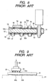
- FIG. 8 is a cross-sectional view showing principal parts of the conventional electronic circuit unit
- Fig. 9 is an explanatory view illustrating the method of fabricating the conventional electronic circuit unit.
- Wiring patterns 52 are formed on the front surface and the rear surface of a circuit board 51 which is composed of a plurality of stacked insulating sheets.
- a solder resist film 53 land units 52b and electrodes 52a exposed from the solder resist film 53 are formed on the wiring pattern 52.
- solder resist film 53 regions of the electrodes 52a and the land units 52b are formed, and the wiring patterns 52 other than the exposed electrodes 52a and land unit 52b are prevented from being broken.
- the solder resist film 53 is formed through printing or deposition of liquefied insulating material, the thickness of a film is not uniform such that an uneven film is formed.
- solder resist film 53 to be formed on both sides of circuit board 51 is prepared.
- solder resist film 53 on the rear surface of the circuit board 51 is placed on the supporting jig 61.
- the circuit board 51 is supported such that the circuit board 51 is tilted against the surface of the supporting jig 61.
- the semiconductor chip 54 is carried onto the electrodes 52a through a mounting jig 62 for absorption and pressing, and the bumps 55 are heated and pressed down to the electrodes 52a by the mounting jig 62.
- the bumps 55 are adhered to the electrodes 52a, and then, the mounting jig 62 return to its original position.
- the pressing of the bumps 55 to the electrodes 52a is performed while being tilted against the circuit board 51, such that some bumps are not sufficiently adhered to the electrodes 52a.
- the semiconductor chip 54 is not sufficiently mounted which leads to an unreliable mounting capability.
- the chip parts 56 are soldered to the land unit 52b by using cream soldering arranged on the land units 52b.
- the chip parts 57 are soldered to the land unit 52b by using cream soldering arranged on the land unit 52b to complete the fabrication process.
- the circuit board 51 since the solder resist film 53 exists on the rear side of the circuit board 51, the circuit board 51 is tilted due to the unevenness of the thickness of the solder resist film 53 during the mount process of the semiconductor chip 54. As a result, the semiconductor chip 54 is not sufficiently mounted which leads to an unreliable mounting.
- An object of the present invention is to provide an electronic circuit unit and a method of fabricating the same with a reliable mounting capability for mounting a semiconductor chip.
- an electronic circuit unit comprising a circuit board composed of a plurality of stacked insulating sheets, a semiconductor chip having a plurality of bumps, in which the plurality of bumps are attached to a plurality of electrodes of wiring patterns arranged on one surface of the circuit board, and chip parts soldered to a plurality of land units arranged on the other surface of the circuit board.
- the circuit board includes a wiring board having the plurality of electrodes arranged on the one surface and a plurality of conducting parts arranged on the other surface, and an insulating plate stacked on the other surface of the wiring board with covering the plurality of conducting parts.
- the land units connected to the conducting parts via connection conductors are arranged, without a solder resist film, on exposed surfaces of the insulating plate which is on the other surface of the circuit board.
- a plurality of conductive patterns may be arranged on the other side of the wiring board, and the conducting parts may be formed as a part of the conductive patterns.
- the wiring board and the insulating plate constituting the circuit board may be made of low temperature co-fired ceramics.
- the respective electrodes of the wiring patterns arranged on the one surface of the wiring board may be formed with the same area, and each of the electrodes may be attached to the bumps to connect the semiconductor chip.
- a method of fabricating an electronic circuit unit comprises a step of preparing a circuit board, in which the circuit board includes a wiring board having a plurality of electrodes of wiring patterns arranged on one surface and a plurality of conducting parts arranged on the other surface, and an insulating plate stacked on the other surface of the wiring board with covering the plurality of conducting parts. Land units are arranged, without a solder resist film, on an exposed surface of the insulating plate and connected to conducting parts through connection conductors.
- the method further comprises a step of mounting the exposed surface of the insulating plate having the land units on a supporting jig on the circuit board, a step of attaching plurality bumps arranged on a semiconductor chip to the electrodes, and a step of soldering chip parts to the land units.
- the wiring board and the insulating plate constituting the circuit board may be made of low temperature co-fired ceramics.
- an electronic circuit unit comprises a circuit board composed of a plurality of stacked insulating sheets; a semiconductor chip having a plurality of bumps, in which the plurality of bumps are attached to a plurality of electrodes of wiring patterns arranged on one surface of the circuit board, and chip parts soldered to a plurality of land units arranged on the other surface of the circuit board.
- the circuit board comprises a wiring board having the plurality of electrodes arranged on the one surface and a plurality of conducting parts arranged on the other surface, and an insulating plate stacked on the other surface of the wiring board with covering the plurality of conducting parts.
- the land units connected to the conducting parts via connection conductors are arranged, without a solder resist film, on an exposed surface of an insulating plate which is on the other surface of the circuit board.
- the electronic circuit unit since the land units connected to the chip parts are arranged on the exposed surface of the insulating plate provided on the rear side of the circuit board in a state where the solder resist film does not exist, the insulating plate where there does not exist the solder resist film can be supported by the supporting jig, and the tilt of the circuit board can be prevented. Therefore, it is ensured that the semiconductor chip is mounted with a reliable mounting capability.
- the conductive patterns are arranged on the rear side of the wiring board and the conducting parts are formed as a part of the conductive patterns, the wiring patterns on the circuit board are readily pulled, and the conductive patterns can be surely prevented from disconnection. Therefore, the circuit board having a high reliability can be obtained.
- the wiring board and the insulating plate constituting the circuit board are made of low temperature co-fired ceramics, the accuracy in the thickness of the circuit board is high and the circuit board having a high flatness of both sides can be obtained.
- the electrodes of the wiring patterns arranged on the one surface of the wiring board have the same area, respectively, and each of the electrodes is adhered to the bump, the electrode area can be identical, so that the area of the soldered bump can be uniformed. Accordingly, the semiconductor chip with a high mounting credibility can be obtained.
- a method of fabricating an electronic circuit unit comprises a step of preparing a circuit board, in which the circuit board includes a wiring board having a plurality of electrodes of wiring patterns arranged on one surface and a plurality of conducting parts arranged on the other surface, and an insulating plate stacked on the other surface of the wiring board, in which a plurality of' land units are arranged, without a solder resist film, on an exposed surface of the insulating plate and connected to a plurality of conducting parts through connection conductors.
- the method further comprises a step of mounting the exposed surface of the insulating plate on the circuit board, having the land units on a supporting jig, a step of attaching plurality bumps arranged on a semiconductor chip to the electrodes, and a step of soldering chip parts to the land units.
- the insulating film where the solder resist film does not exist is supported by the supporting jig during the mounting process of the semiconductor chip.
- the circuit board is not tilted against the surface of the supporting jig so that it is ensured that the semiconductor chip is mounted with a reliable mounting capability.
- the wiring board and the insulating plate constituting the circuit board are made of low temperature co-fired ceramics, the accuracy in the thickness of the circuit board is high and the circuit board having a high flatness of both sides can be obtained.
- FIG. 1 is a front view of the electronic circuit unit of the present invention
- Fig. 2 is a cross-sectional view showing principle parts of the electronic circuit unit of the present invention
- Fig. 3 is a plan view of a circuit board of the electronic circuit unit of the present invention
- Fig. 4 is a bottom view of the circuit board of the electronic circuit unit of the present invention.
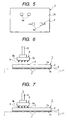
- Fig. 5 is a bottom view of a wiring board constituting the circuit board according to the electronic circuit unit of the present invention
- Fig. 6 is a diagram for illustrating a first step according to the method of fabricating the electronic circuit unit of the present invention
- Fig. 7 is a diagram for illustrating a second step according to the method of fabricating the electronic circuit unit of the present invention.
- a circuit board 1 is composed of a plurality of insulating sheets made of low temperature co-fired ceramics (LTCC) or a resin, and includes a wiring board 2 arranged on an upper side and an insulating plate 3 stacked on the lower side of the wiring board 2.
- LTCC low temperature co-fired ceramics
- circuit board 1 made of low temperature co-fired ceramics, since a green sheet is pressed and co-fired, it is possible to provide the circuit board 1 with a high precision.
- wiring patterns 4 and a plurality of electrodes 5 are arranged, and at the same time, exposed regions of the electrodes 5 are formed by a solder resist film, though not shown, and the wiring patterns 4 are protected from dusts.
- conductive patterns 6 are formed, as shown in Fig. 5, and conducting parts 6a which is formed as a portion of the conductive patterns 6 are also arranged.
- the conductive patterns 6 and the conducting parts 6a are covered with the insulating plate 3.
- the conductive patterns 6 and the conducting parts 6a contact with the wiring patterns 4 arranged on the upper surface 1a, at appropriate positions.
- land units 7 are arranged, and the land units 7 are connected to the conducting parts 6a through connection conductors (through-holes) 13.
- the land units 7 are arranged on the lower exposed surface of the insulating plate 3, which is the rear surface 1b of the circuit board 1, without the solder resist film.
- a semiconductor chip 8 composed of a flip chip and the like comprises a body unit 8a and a plurality of electrodes unit 8b arranged on the rear surface of the body unit 8a, and the electrodes unit 8b are pressed and adhered to bumps composed of balls and the like with soldering film on the outer surface.
- the bumps 9 arranged on the semiconductor chip 8 are pressed (attached) to the electrodes 5, such that the semiconductor chip 8 is mounted on the circuit board 1.
- the chip part 10 composed of capacitors or resistors are soldered to the land units 7, such that the chip parts 10 are mounted on the circuit board 1.
- the chip parts such as capacitors may be soldered to the wiring patterns 4, such that an electronic circuit unit of the present invention can be provided.
- the solder resist film does not exist on the rear surface 1b of the circuit board 1, and thus, the land units 7 are arranged on the surface of the supporting jig 11 with a high precision, the circuit board is supported such that the circuit board 1 is parallel with the surface of the supporting jig 11.
- the semiconductor chip 8 is carried on the electrodes 5. Then, as shown in Fig. 7, by moving the mounting jig 12 downwardly, the bumps 9 are pressed down and adhered to the electrodes 5.
- the mounting jig 12 returns to its original position.
- the chip parts 10 are soldered to the land unit 7 using cream solder arranged on the land units 7 to complete the fabrication process.
- the land units 7 for connecting the chip parts 10 are arranged, without the solder resist film, on the exposed surface of the insulating plate 3 which is on the rear surface 1b of the circuit board 1, the insulating plate 3 where the solder resist film does not exist can be supported by the supporting jig 11 during the mounting process of the semiconductor chip 8, such that the circuit board 1 is not tilted. Therefore, it is ensured the semiconductor chip 8 is mounted with a reliable mounting capability can be obtained.
Landscapes
- Engineering & Computer Science (AREA)
- Microelectronics & Electronic Packaging (AREA)
- Electric Connection Of Electric Components To Printed Circuits (AREA)
- Wire Bonding (AREA)
- Structures For Mounting Electric Components On Printed Circuit Boards (AREA)
Applications Claiming Priority (4)
| Application Number | Priority Date | Filing Date | Title |
|---|---|---|---|
| JP2003429217 | 2003-12-25 | ||
| JP2003429217 | 2003-12-25 | ||
| JP2004303909 | 2004-10-19 | ||
| JP2004303909A JP4343082B2 (ja) | 2003-12-25 | 2004-10-19 | 電子回路ユニット、及びその製造方法 |
Publications (2)
| Publication Number | Publication Date |
|---|---|
| EP1549119A2 true EP1549119A2 (de) | 2005-06-29 |
| EP1549119A3 EP1549119A3 (de) | 2007-08-08 |
Family
ID=34554864
Family Applications (1)
| Application Number | Title | Priority Date | Filing Date |
|---|---|---|---|
| EP04030634A Withdrawn EP1549119A3 (de) | 2003-12-25 | 2004-12-23 | Elektronische Schaltungseinheit und Verfahren zu deren Herstellung |
Country Status (3)
| Country | Link |
|---|---|
| US (1) | US7157362B2 (de) |
| EP (1) | EP1549119A3 (de) |
| JP (1) | JP4343082B2 (de) |
Family Cites Families (17)
| Publication number | Priority date | Publication date | Assignee | Title |
|---|---|---|---|---|
| US6097089A (en) * | 1998-01-28 | 2000-08-01 | Mitsubishi Gas Chemical Company, Inc. | Semiconductor plastic package, metal plate for said package, and method of producing copper-clad board for said package |
| US4740414A (en) * | 1986-11-17 | 1988-04-26 | Rockwell International Corporation | Ceramic/organic multilayer interconnection board |
| US4910643A (en) * | 1988-06-06 | 1990-03-20 | General Electric Company | Thick film, multi-layer, ceramic interconnected circuit board |
| JPH05243330A (ja) * | 1992-02-28 | 1993-09-21 | Nippondenso Co Ltd | 多層配線基板とフリップチップicの接続構造 |
| JP3081559B2 (ja) * | 1997-06-04 | 2000-08-28 | ニッコー株式会社 | ボールグリッドアレイ型半導体装置およびその製造方法ならびに電子装置 |
| US6222246B1 (en) * | 1999-01-08 | 2001-04-24 | Intel Corporation | Flip-chip having an on-chip decoupling capacitor |
| US20030038366A1 (en) * | 1999-03-09 | 2003-02-27 | Kabushiki Kaisha Toshiba | Three-dimensional semiconductor device having plural active semiconductor components |
| JP3792445B2 (ja) * | 1999-03-30 | 2006-07-05 | 日本特殊陶業株式会社 | コンデンサ付属配線基板 |
| JP2000307212A (ja) | 1999-04-20 | 2000-11-02 | Denso Corp | 配線基板及びその製造方法 |
| JP3585793B2 (ja) * | 1999-11-09 | 2004-11-04 | 富士通株式会社 | 両面薄膜配線基板の製造方法 |
| JP3531573B2 (ja) * | 2000-03-17 | 2004-05-31 | 株式会社村田製作所 | 積層型セラミック電子部品およびその製造方法ならびに電子装置 |
| JP2002134873A (ja) * | 2000-10-24 | 2002-05-10 | Nippon Dempa Kogyo Co Ltd | チップ素子の実装方法及び表面実装用の水晶発振器 |
| JP2003124429A (ja) * | 2001-10-15 | 2003-04-25 | Matsushita Electric Ind Co Ltd | モジュール部品 |
| JP2003264253A (ja) * | 2002-03-12 | 2003-09-19 | Shinko Electric Ind Co Ltd | 半導体装置及びその製造方法 |
| DE10228328A1 (de) * | 2002-06-25 | 2004-01-22 | Epcos Ag | Elektronisches Bauelement mit einem Mehrlagensubstrat und Herstellungsverfahren |
| US20040022038A1 (en) * | 2002-07-31 | 2004-02-05 | Intel Corporation | Electronic package with back side, cavity mounted capacitors and method of fabrication therefor |
| JP4105524B2 (ja) * | 2002-10-23 | 2008-06-25 | 株式会社東芝 | 半導体装置 |
-
2004
- 2004-10-19 JP JP2004303909A patent/JP4343082B2/ja not_active Expired - Fee Related
- 2004-12-21 US US11/020,618 patent/US7157362B2/en not_active Expired - Lifetime
- 2004-12-23 EP EP04030634A patent/EP1549119A3/de not_active Withdrawn
Also Published As
| Publication number | Publication date |
|---|---|
| US20050140008A1 (en) | 2005-06-30 |
| EP1549119A3 (de) | 2007-08-08 |
| US7157362B2 (en) | 2007-01-02 |
| JP2005210068A (ja) | 2005-08-04 |
| JP4343082B2 (ja) | 2009-10-14 |
Similar Documents
| Publication | Publication Date | Title |
|---|---|---|
| US7019221B1 (en) | Printed wiring board | |
| JPH11307886A (ja) | フリップチップ接合ランドうねり防止パターン | |
| US20070035021A1 (en) | Printed circuit board and electronic apparatus including printed circuit board | |
| US20070169342A1 (en) | Connection pad layouts | |
| JP2005050891A (ja) | フレキシブル配線基板、半導体チップ実装フレキシブル配線基板、表示装置、半導体チップ実装方法 | |
| JP2001168131A (ja) | 薄型相互接続構造 | |
| JPH06120670A (ja) | 多層配線基板 | |
| JP2003124595A (ja) | 電子回路ユニット | |
| JPH11233684A (ja) | 半導体装置用基板、半導体装置及びその製造方法並びに電子機器 | |
| JP2010219180A (ja) | 電子部品実装構造および電子部品実装方法ならびに基板接続用部品 | |
| US7063797B2 (en) | Mounting electronic components | |
| JP5202567B2 (ja) | 電子部品実装方法 | |
| US7157362B2 (en) | Electronic circuit unit and method of fabricating the same | |
| US6870260B2 (en) | Semiconductor module | |
| JP2873645B2 (ja) | セラミック多層配線基板の製造方法 | |
| GB2412790A (en) | Process for the assembly of electronic devices | |
| JP2002076629A (ja) | 複合多層配線基板 | |
| EP0343379A2 (de) | Dünnschichtpackung für eine gemischte Chipverbindung | |
| JP2002280704A (ja) | 表面実装用電子部品の実装構造および実装方法 | |
| JP2002280681A (ja) | 部品実装基板の製造方法、およびプリント配線板 | |
| JPH1167945A (ja) | 電子回路モジュール | |
| JPH1022412A (ja) | ボールグリッドアレイ型回路基板 | |
| JP2004056082A (ja) | 配線基板およびその製造方法 | |
| JPH06140465A (ja) | 回路部品搭載用中間基板及びその製造法 | |
| JP2003318503A (ja) | 多層電子回路基板及びこれを搭載した電子機器 |
Legal Events
| Date | Code | Title | Description |
|---|---|---|---|
| PUAI | Public reference made under article 153(3) epc to a published international application that has entered the european phase |
Free format text: ORIGINAL CODE: 0009012 |
|
| AK | Designated contracting states |
Kind code of ref document: A2 Designated state(s): AT BE BG CH CY CZ DE DK EE ES FI FR GB GR HU IE IS IT LI LT LU MC NL PL PT RO SE SI SK TR |
|
| AX | Request for extension of the european patent |
Extension state: AL BA HR LV MK YU |
|
| PUAL | Search report despatched |
Free format text: ORIGINAL CODE: 0009013 |
|
| AK | Designated contracting states |
Kind code of ref document: A3 Designated state(s): AT BE BG CH CY CZ DE DK EE ES FI FR GB GR HU IE IS IT LI LT LU MC NL PL PT RO SE SI SK TR |
|
| AX | Request for extension of the european patent |
Extension state: AL BA HR LV MK YU |
|
| RIC1 | Information provided on ipc code assigned before grant |
Ipc: H05K 3/46 20060101ALN20070629BHEP Ipc: H05K 3/34 20060101ALN20070629BHEP Ipc: H01L 25/16 20060101ALI20070629BHEP Ipc: H05K 1/18 20060101ALI20070629BHEP Ipc: H05K 1/11 20060101AFI20050329BHEP |
|
| 17P | Request for examination filed |
Effective date: 20070731 |
|
| AKX | Designation fees paid |
Designated state(s): DE FR GB |
|
| 17Q | First examination report despatched |
Effective date: 20120502 |
|
| STAA | Information on the status of an ep patent application or granted ep patent |
Free format text: STATUS: THE APPLICATION IS DEEMED TO BE WITHDRAWN |
|
| 18D | Application deemed to be withdrawn |
Effective date: 20120913 |