EP1548848A1 - Solarzelle aus amorphem Silizium - Google Patents
Solarzelle aus amorphem Silizium Download PDFInfo
- Publication number
- EP1548848A1 EP1548848A1 EP05001765A EP05001765A EP1548848A1 EP 1548848 A1 EP1548848 A1 EP 1548848A1 EP 05001765 A EP05001765 A EP 05001765A EP 05001765 A EP05001765 A EP 05001765A EP 1548848 A1 EP1548848 A1 EP 1548848A1
- Authority
- EP
- European Patent Office
- Prior art keywords
- amorphous silicon
- layer
- power
- solar cell
- type
- Prior art date
- Legal status (The legal status is an assumption and is not a legal conclusion. Google has not performed a legal analysis and makes no representation as to the accuracy of the status listed.)
- Withdrawn
Links
- 229910021417 amorphous silicon Inorganic materials 0.000 title claims abstract description 51
- 230000007547 defect Effects 0.000 claims abstract description 35
- 239000000758 substrate Substances 0.000 claims abstract description 34
- 230000006641 stabilisation Effects 0.000 description 13
- 238000011105 stabilization Methods 0.000 description 13
- 239000007789 gas Substances 0.000 description 12
- 230000003287 optical effect Effects 0.000 description 7
- 230000015556 catabolic process Effects 0.000 description 6
- 230000007423 decrease Effects 0.000 description 6
- 238000006731 degradation reaction Methods 0.000 description 6
- BLRPTPMANUNPDV-UHFFFAOYSA-N Silane Chemical compound [SiH4] BLRPTPMANUNPDV-UHFFFAOYSA-N 0.000 description 5
- 238000010521 absorption reaction Methods 0.000 description 4
- 230000003247 decreasing effect Effects 0.000 description 4
- 239000011521 glass Substances 0.000 description 4
- 238000005268 plasma chemical vapour deposition Methods 0.000 description 4
- 238000010276 construction Methods 0.000 description 3
- 230000015572 biosynthetic process Effects 0.000 description 2
- 238000001816 cooling Methods 0.000 description 2
- 230000000694 effects Effects 0.000 description 2
- 238000011109 contamination Methods 0.000 description 1
- 239000003599 detergent Substances 0.000 description 1
- ZOCHARZZJNPSEU-UHFFFAOYSA-N diboron Chemical compound B#B ZOCHARZZJNPSEU-UHFFFAOYSA-N 0.000 description 1
- 238000010438 heat treatment Methods 0.000 description 1
- 230000031700 light absorption Effects 0.000 description 1
- 238000004519 manufacturing process Methods 0.000 description 1
- 239000000463 material Substances 0.000 description 1
- 239000002184 metal Substances 0.000 description 1
- 230000007935 neutral effect Effects 0.000 description 1
- 238000010248 power generation Methods 0.000 description 1
- HBMJWWWQQXIZIP-UHFFFAOYSA-N silicon carbide Chemical compound [Si+]#[C-] HBMJWWWQQXIZIP-UHFFFAOYSA-N 0.000 description 1
- XOLBLPGZBRYERU-UHFFFAOYSA-N tin dioxide Chemical compound O=[Sn]=O XOLBLPGZBRYERU-UHFFFAOYSA-N 0.000 description 1
- 229910001887 tin oxide Inorganic materials 0.000 description 1
- 229910021642 ultra pure water Inorganic materials 0.000 description 1
- 239000012498 ultrapure water Substances 0.000 description 1
- 238000007740 vapor deposition Methods 0.000 description 1
Images


Classifications
-
- H—ELECTRICITY
- H10—SEMICONDUCTOR DEVICES; ELECTRIC SOLID-STATE DEVICES NOT OTHERWISE PROVIDED FOR
- H10F—INORGANIC SEMICONDUCTOR DEVICES SENSITIVE TO INFRARED RADIATION, LIGHT, ELECTROMAGNETIC RADIATION OF SHORTER WAVELENGTH OR CORPUSCULAR RADIATION
- H10F77/00—Constructional details of devices covered by this subclass
- H10F77/10—Semiconductor bodies
- H10F77/12—Active materials
- H10F77/122—Active materials comprising only Group IV materials
-
- H—ELECTRICITY
- H10—SEMICONDUCTOR DEVICES; ELECTRIC SOLID-STATE DEVICES NOT OTHERWISE PROVIDED FOR
- H10F—INORGANIC SEMICONDUCTOR DEVICES SENSITIVE TO INFRARED RADIATION, LIGHT, ELECTROMAGNETIC RADIATION OF SHORTER WAVELENGTH OR CORPUSCULAR RADIATION
- H10F10/00—Individual photovoltaic cells, e.g. solar cells
- H10F10/10—Individual photovoltaic cells, e.g. solar cells having potential barriers
- H10F10/17—Photovoltaic cells having only PIN junction potential barriers
-
- H—ELECTRICITY
- H10—SEMICONDUCTOR DEVICES; ELECTRIC SOLID-STATE DEVICES NOT OTHERWISE PROVIDED FOR
- H10F—INORGANIC SEMICONDUCTOR DEVICES SENSITIVE TO INFRARED RADIATION, LIGHT, ELECTROMAGNETIC RADIATION OF SHORTER WAVELENGTH OR CORPUSCULAR RADIATION
- H10F71/00—Manufacture or treatment of devices covered by this subclass
- H10F71/10—Manufacture or treatment of devices covered by this subclass the devices comprising amorphous semiconductor material
- H10F71/103—Manufacture or treatment of devices covered by this subclass the devices comprising amorphous semiconductor material including only Group IV materials
-
- H—ELECTRICITY
- H10—SEMICONDUCTOR DEVICES; ELECTRIC SOLID-STATE DEVICES NOT OTHERWISE PROVIDED FOR
- H10F—INORGANIC SEMICONDUCTOR DEVICES SENSITIVE TO INFRARED RADIATION, LIGHT, ELECTROMAGNETIC RADIATION OF SHORTER WAVELENGTH OR CORPUSCULAR RADIATION
- H10F77/00—Constructional details of devices covered by this subclass
- H10F77/10—Semiconductor bodies
- H10F77/16—Material structures, e.g. crystalline structures, film structures or crystal plane orientations
- H10F77/162—Non-monocrystalline materials, e.g. semiconductor particles embedded in insulating materials
- H10F77/166—Amorphous semiconductors
- H10F77/1662—Amorphous semiconductors including only Group IV materials
-
- Y—GENERAL TAGGING OF NEW TECHNOLOGICAL DEVELOPMENTS; GENERAL TAGGING OF CROSS-SECTIONAL TECHNOLOGIES SPANNING OVER SEVERAL SECTIONS OF THE IPC; TECHNICAL SUBJECTS COVERED BY FORMER USPC CROSS-REFERENCE ART COLLECTIONS [XRACs] AND DIGESTS
- Y02—TECHNOLOGIES OR APPLICATIONS FOR MITIGATION OR ADAPTATION AGAINST CLIMATE CHANGE
- Y02E—REDUCTION OF GREENHOUSE GAS [GHG] EMISSIONS, RELATED TO ENERGY GENERATION, TRANSMISSION OR DISTRIBUTION
- Y02E10/00—Energy generation through renewable energy sources
- Y02E10/50—Photovoltaic [PV] energy
- Y02E10/547—Monocrystalline silicon PV cells
-
- Y—GENERAL TAGGING OF NEW TECHNOLOGICAL DEVELOPMENTS; GENERAL TAGGING OF CROSS-SECTIONAL TECHNOLOGIES SPANNING OVER SEVERAL SECTIONS OF THE IPC; TECHNICAL SUBJECTS COVERED BY FORMER USPC CROSS-REFERENCE ART COLLECTIONS [XRACs] AND DIGESTS
- Y02—TECHNOLOGIES OR APPLICATIONS FOR MITIGATION OR ADAPTATION AGAINST CLIMATE CHANGE
- Y02E—REDUCTION OF GREENHOUSE GAS [GHG] EMISSIONS, RELATED TO ENERGY GENERATION, TRANSMISSION OR DISTRIBUTION
- Y02E10/00—Energy generation through renewable energy sources
- Y02E10/50—Photovoltaic [PV] energy
- Y02E10/548—Amorphous silicon PV cells
-
- Y—GENERAL TAGGING OF NEW TECHNOLOGICAL DEVELOPMENTS; GENERAL TAGGING OF CROSS-SECTIONAL TECHNOLOGIES SPANNING OVER SEVERAL SECTIONS OF THE IPC; TECHNICAL SUBJECTS COVERED BY FORMER USPC CROSS-REFERENCE ART COLLECTIONS [XRACs] AND DIGESTS
- Y02—TECHNOLOGIES OR APPLICATIONS FOR MITIGATION OR ADAPTATION AGAINST CLIMATE CHANGE
- Y02P—CLIMATE CHANGE MITIGATION TECHNOLOGIES IN THE PRODUCTION OR PROCESSING OF GOODS
- Y02P70/00—Climate change mitigation technologies in the production process for final industrial or consumer products
- Y02P70/50—Manufacturing or production processes characterised by the final manufactured product
Definitions
- the present invention relates to an amorphous silicon solar cell used in a solar cell power generation system.
- Patent No. 2530408 The arrangement shown in FIG. 3 (Patent No. 2530408) is known as a conventional solar cell.
- a transparent electrode 2, a power-generating film 3, and a metal electrode 4 are formed in this order on a glass substrate (or transparent film) 1.
- the power-generating film 3 is constructed of a p-type a-Si x C 1-x :H layer ( p layer) 5, an i-type a-SiH layer ( i layer) 6, and an n-type a-Si:H layer ( n layer) 7.
- the p layer 5 as a window layer is made of amorphous silicon carbide to increase its optical forbidden band width.
- diborane (B 2 H 6 ) is added as a doping gas to the source gas in the formation of the p layer 5.
- the film properties of this i layer 6 have a direct influence on the characteristics of the solar cell.
- the output current of the solar cell is determined by the light absorption characteristic and film thickness of the solar cell material. That is, if the absorption coefficient is small, the film thickness must be increased; if the absorption coefficient is large, the film thickness can be small.
- the absorption coefficient to light of 500 to 700 nm having the greatest influence on the output current increases as the number of defects in the amorphous silicon film forming the i layer 6 decreases, i.e., as the number of unbonded hands of Si decreases.
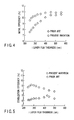
- the film thickness of the i layer 6 must be 400 nm or more to increase the initial efficiency as shown in FIG. 4. However, if the film thickness of the i layer 6 is thus increased, a long time is required to form this i layer 6, lowering the productivity.
- the stabilization efficiency declines because the rate of optical degradation increases.
- the film thickness of the i layer 6 is decreased, the degradation rate decreases.
- the stabilization efficiency does not increase because the initial efficiency is small.
- an amorphous silicon solar cell comprising a transparent substrate, a transparent electrode formed on the transparent substrate, a power-generating film formed on the transparent electrode, and a back-side electrode formed on the power-generating film, characterized in that the power-generating film is formed by sequentially stacking p-type/i-type/n-type hydrogenated amorphous silicon layers, and a defect density in the i-type hydrogenated amorphous silicon layer is less than 10 15 defects/cc.
- an amorphous silicon solar cell comprising a substrate, a transparent electrode formed on the substrate, a power-generating film formed on the transparent electrode, and a back-side electrode formed on the power-generating film, characterized in that the power-generating film is formed by sequentially stacking n-type/i-type/p-type hydrogenated amorphous silicon layers, and a defect density in the i-type hydrogenated amorphous silicon layer is less than 10 15 defects/cc.
- An amorphous silicon solar cell comprises a transparent substrate, a transparent electrode formed on the transparent substrate, a power-generating film formed on the transparent electrode, and a back-side electrode formed on the power-generating film, characterized in that the power-generating film is formed by sequentially stacking p-type/i-type/n-type hydrogenated amorphous silicon layers, and a defect density in the i-type hydrogenated amorphous silicon layer is less than 10 15 defects/cc.
- an amorphous silicon solar cell comprises a substrate, a transparent electrode formed on the substrate, a power-generating film formed on the transparent electrode, and a back-side electrode formed on the power-generating film, characterized in that the power-generating film is formed by sequentially stacking n-type/i-type/p-type hydrogenated amorphous silicon layers, and a defect density in the i-type hydrogenated amorphous silicon layer is less than 10 15 defects/cc.
- the defect density in the i-type hydrogenated amorphous silicon layer ( i layer) is prescribed to be less than 10 15 defects/cc because if the defect density has a larger value, the stabilization defect density after light irradiation increases, so no high stabilization efficiency can be obtained when this layer is applied to the cell.
- "Stabilization" means 20 to 100 hr.
- the i layer thickness is preferably 300 nm or less because when the thickness is 300 nm or less, the optical degradation rate decreases, and this increases the efficiency (FIGS. 4 and 5).
- This optical degradation rate is defined by (initial efficiency - stabilization efficiency) ⁇ initial efficiency. Comparing FIG. 4 with FIG. 5 shows that the optical degradation rate declines as the i layer film thickness decreases.
- FIG. 4 also indicates that a film having large defect density (10 15 defects/cc or more) produces a large reduction in the initial efficiency when the i layer film thickness decreases. However, this reduction is small in the film of the present invention. As a result, the aforementioned condition is derived.
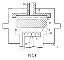
- FIG. 8 is a sectional view showing the major parts of a plasma CVD apparatus according to the present invention.
- reference numeral 31 denotes a plasma chamber.
- a substrate holder 33 supporting a substrate 32 is placed in this chamber 31.
- the substrate holder 33 contains a substrate heater 34 for heating the substrate 32 and a thermocouple 35 for controlling the temperature of the substrate heater 34.
- This substrate heater 34 controls the temperature of the substrate 32.
- a water-cooling mechanism (not shown) for cooling the substrate heater 34 is built into the substrate heater 34.
- a mesh like second heater 36 is positioned above the substrate holder 33 in the chamber 31.
- An RF electrode 37 is placed on the side of the second heater 36 away from the side opposite to the substrate holder 33 with the heater 34 sandwiched between them.
- This RF electrode 37 has a gas supply pipe 38.
- a gas supply hole 39 for supplying a gas into the plasma chamber 31 is formed in the surface of the RF electrode 32 that faces the second heater 36.
- reference numeral 40 denotes
- the plasma CVD apparatus with this construction is generally used by using a monosilane (SiH 4 ) gas as a gas at a flow rate of 20 to 100 sccm, a pressure of 50 to 200 mTorr, an RF power of 5 to 60W, and a substrate temperature of 160 to 200°C.
- a monosilane (SiH 4 ) gas as a gas at a flow rate of 20 to 100 sccm, a pressure of 50 to 200 mTorr, an RF power of 5 to 60W, and a substrate temperature of 160 to 200°C.
- FIG. 1 will be described below.
- a tin oxide transparent electrode 12 is formed on a glass substrate 11 as a transparent substrate.
- a power-generating film 16 constructed of a p layer 13, an i layer 14, and an n layer 15 is formed on the transparent electrode 12.
- Each of these p , i , and n layers 13, 14, and 15 is a hydrogenated amorphous silicon (a-Si:H) layer.
- the thickness of the i layer 13 is 300 nm or less, e.g., 290 nm, and its defect density is less than 10 15 defects/cc.
- An Al back-side electrode 17 is formed on the power-generating film 16.
- the amorphous silicon solar cell with this construction is manufactured as follows by using the abovementioned apparatus shown in FIG. 8.
- a glass substrate 11 on which a transparent electrode 12 was formed was ultrasonically cleaned with a neutral detergent and ultra pure water in this order to remove contamination adhered to the surfaces.
- a power-generating film 16 constructed of a p layer 13, an i layer 14, and an n layer 15 was formed on this transparent electrode 12 by plasma CVD.
- the apparatus was evacuated by a turbo molecular pump until the internal pressure of the apparatus decreased to 5 ⁇ 10 -7 Torr or less, and the substrate temperature was raised to and maintained at a predetermined temperature (150°C to 180°C).
- the p layer was formed by using SiH 4 , CH 4 , and H 2 as source gases and B 2 H 6 as a doping gas.
- the i layer was formed by using SiH 4 as a source gas.
- the n layer was formed by using SiH 4 and H 2 as source gases and PH 3 as a doping gas.
- the film thicknesses of these p , i , and n layers were 9.5 nm, 290 nm, and 30 nm, respectively.
- the back-side electrode 17 was formed on this power-generating film 16 by vacuum vapor deposition, thereby manufacturing an amorphous silicon solar cell.
- the amorphous silicon solar cell manufactured as above has the following effects.
- the i layer 14 forming the power-generating film 17 is a hydrogenated amorphous silicon layer having a defect density of less than 10 15 defects/cc. Therefore, as shown in FIG. 6, the stabilization defect density after light irradiation is smaller than that of a conventional film. Hence, a high stabilization coefficient can be obtained when this layer is applied to the cell. Also, this low-defect-density film has a large absorption coefficient to long-wavelength light (500 to 700 nm). Accordingly, even when the thickness of the i layer 14 is decreased (290 nm in the present invention, while the conventional film thickness is about 400 to 500 nm), a reduction of the output current is small, so high efficiency can be obtained (FIGS. 3 and 6).
- the productivity can also be increased. In effect, when the thickness of the i layer 14 was 300 nm, which was about 3/4 the conventional film thickness (400 to 500 nm), the productivity improved by about 20%. (Example 2)
- FIG. 2 will be described below.
- An Ag transparent electrode 22 is formed on a stainless substrate 21.
- a power-generating film 26 constructed of an n layer 23, an i layer 24, and a p layer 25 is formed on this transparent electrode 22.
- Each of these n , i , and p layers 23, 24, and 25 is a hydrogenated amorphous silicon (a-Si:H) layer.
- the thickness of the i layer 24 is 300 nm or less, e.g., 290 nm, and its defect density is less than 10 15 defects/cc.
- An ITO transparent back-side electrode 27 is formed on the power-generating film 26.
- Example 2 can achieve high stabilization efficiency and increase the productivity.
- an amorphous silicon solar cell in which the defect density of an i-type hydrogenated amorphous silicon layer forming a power-generating layer is less than 10 15 defects/cc and which thereby can raise the initial efficiency without lowering the productivity and achieve high stabilization efficiency compared to conventional solar cells.
- the present invention can also provide an amorphous silicon solar cell in which the thickness of an i-type hydrogenated amorphous silicon layer is 300 nm or less and which thereby can improve the productivity compared to conventional solar cells.
Landscapes
- Photovoltaic Devices (AREA)
Applications Claiming Priority (5)
| Application Number | Priority Date | Filing Date | Title |
|---|---|---|---|
| JP937799 | 1999-01-18 | ||
| JP937799 | 1999-01-18 | ||
| JP23550999 | 1999-08-23 | ||
| JP23550999A JP3364180B2 (ja) | 1999-01-18 | 1999-08-23 | 非晶質シリコン太陽電池 |
| EP99118281A EP1020931A1 (de) | 1999-01-18 | 1999-09-15 | Solarzelle aus amorphem Silizium |
Related Parent Applications (1)
| Application Number | Title | Priority Date | Filing Date |
|---|---|---|---|
| EP99118281A Division EP1020931A1 (de) | 1999-01-18 | 1999-09-15 | Solarzelle aus amorphem Silizium |
Publications (1)
| Publication Number | Publication Date |
|---|---|
| EP1548848A1 true EP1548848A1 (de) | 2005-06-29 |
Family
ID=26344073
Family Applications (2)
| Application Number | Title | Priority Date | Filing Date |
|---|---|---|---|
| EP99118281A Ceased EP1020931A1 (de) | 1999-01-18 | 1999-09-15 | Solarzelle aus amorphem Silizium |
| EP05001765A Withdrawn EP1548848A1 (de) | 1999-01-18 | 1999-09-15 | Solarzelle aus amorphem Silizium |
Family Applications Before (1)
| Application Number | Title | Priority Date | Filing Date |
|---|---|---|---|
| EP99118281A Ceased EP1020931A1 (de) | 1999-01-18 | 1999-09-15 | Solarzelle aus amorphem Silizium |
Country Status (4)
| Country | Link |
|---|---|
| US (1) | US6307146B1 (de) |
| EP (2) | EP1020931A1 (de) |
| JP (1) | JP3364180B2 (de) |
| AU (1) | AU732181B2 (de) |
Cited By (1)
| Publication number | Priority date | Publication date | Assignee | Title |
|---|---|---|---|---|
| CN101834221B (zh) * | 2009-03-13 | 2012-08-22 | 北京北方微电子基地设备工艺研究中心有限责任公司 | 薄膜太阳能电池吸收层的制备方法 |
Families Citing this family (26)
| Publication number | Priority date | Publication date | Assignee | Title |
|---|---|---|---|---|
| US7655542B2 (en) * | 2006-06-23 | 2010-02-02 | Applied Materials, Inc. | Methods and apparatus for depositing a microcrystalline silicon film for photovoltaic device |
| JP2008066437A (ja) * | 2006-09-06 | 2008-03-21 | Mitsubishi Heavy Ind Ltd | 太陽電池パネルの製造方法 |
| US8203071B2 (en) * | 2007-01-18 | 2012-06-19 | Applied Materials, Inc. | Multi-junction solar cells and methods and apparatuses for forming the same |
| US7582515B2 (en) * | 2007-01-18 | 2009-09-01 | Applied Materials, Inc. | Multi-junction solar cells and methods and apparatuses for forming the same |
| US20080173350A1 (en) * | 2007-01-18 | 2008-07-24 | Applied Materials, Inc. | Multi-junction solar cells and methods and apparatuses for forming the same |
| US20080223440A1 (en) * | 2007-01-18 | 2008-09-18 | Shuran Sheng | Multi-junction solar cells and methods and apparatuses for forming the same |
| US20080245414A1 (en) * | 2007-04-09 | 2008-10-09 | Shuran Sheng | Methods for forming a photovoltaic device with low contact resistance |
| US7875486B2 (en) * | 2007-07-10 | 2011-01-25 | Applied Materials, Inc. | Solar cells and methods and apparatuses for forming the same including I-layer and N-layer chamber cleaning |
| US20090104733A1 (en) * | 2007-10-22 | 2009-04-23 | Yong Kee Chae | Microcrystalline silicon deposition for thin film solar applications |
| CN101842875A (zh) | 2007-11-02 | 2010-09-22 | 应用材料股份有限公司 | 在沉积处理间实施的等离子处理 |
| US20090211623A1 (en) * | 2008-02-25 | 2009-08-27 | Suniva, Inc. | Solar module with solar cell having crystalline silicon p-n homojunction and amorphous silicon heterojunctions for surface passivation |
| US8076175B2 (en) * | 2008-02-25 | 2011-12-13 | Suniva, Inc. | Method for making solar cell having crystalline silicon P-N homojunction and amorphous silicon heterojunctions for surface passivation |
| US20110180124A1 (en) * | 2008-08-19 | 2011-07-28 | Oerlikon Solar Ag, Truebbach | Photovoltaic cell and method of manufacturing a photovoltaic cell |
| US8895842B2 (en) * | 2008-08-29 | 2014-11-25 | Applied Materials, Inc. | High quality TCO-silicon interface contact structure for high efficiency thin film silicon solar cells |
| US20100059110A1 (en) * | 2008-09-11 | 2010-03-11 | Applied Materials, Inc. | Microcrystalline silicon alloys for thin film and wafer based solar applications |
| JP4875725B2 (ja) * | 2009-05-11 | 2012-02-15 | 三菱重工業株式会社 | 薄膜シリコン積層型太陽電池の製造方法 |
| WO2011011301A2 (en) * | 2009-07-23 | 2011-01-27 | Applied Materials, Inc. | A mixed silicon phase film for high efficiency thin film silicon solar cells |
| EP2312641A1 (de) * | 2009-10-13 | 2011-04-20 | Ecole Polytechnique Fédérale de Lausanne (EPFL) | Vorrichtung mit elektrischen Kontakten und deren Herstellungsverfahren |
| WO2011046664A2 (en) * | 2009-10-15 | 2011-04-21 | Applied Materials, Inc. | A barrier layer disposed between a substrate and a transparent conductive oxide layer for thin film silicon solar cells |
| US20110088760A1 (en) * | 2009-10-20 | 2011-04-21 | Applied Materials, Inc. | Methods of forming an amorphous silicon layer for thin film solar cell application |
| US20110100447A1 (en) * | 2009-11-04 | 2011-05-05 | General Electric Company | Layer for thin film photovoltaics and a solar cell made therefrom |
| US20110126875A1 (en) * | 2009-12-01 | 2011-06-02 | Hien-Minh Huu Le | Conductive contact layer formed on a transparent conductive layer by a reactive sputter deposition |
| US20110232753A1 (en) * | 2010-03-23 | 2011-09-29 | Applied Materials, Inc. | Methods of forming a thin-film solar energy device |
| JP4775869B1 (ja) | 2010-05-27 | 2011-09-21 | シャープ株式会社 | 光電変換装置 |
| KR20120111657A (ko) * | 2011-04-01 | 2012-10-10 | 삼성전자주식회사 | 태양 전지 |
| US20140124014A1 (en) | 2012-11-08 | 2014-05-08 | Cogenra Solar, Inc. | High efficiency configuration for solar cell string |
Citations (4)
| Publication number | Priority date | Publication date | Assignee | Title |
|---|---|---|---|---|
| EP0135294A2 (de) * | 1983-07-18 | 1985-03-27 | Energy Conversion Devices, Inc. | Legierungen niedrigen Bandabstandes für fotovoltaische Anwendungen |
| US4839701A (en) * | 1985-06-03 | 1989-06-13 | Toyo Boseki Kabushiki Kaisha | Hydrogenated amorphous silicon film |
| US5114498A (en) * | 1989-03-31 | 1992-05-19 | Sanyo Electric Co., Ltd. | Photovoltaic device |
| US5736431A (en) * | 1995-02-28 | 1998-04-07 | Semiconductor Energy Laboratory Co., Ltd. | Method for producing thin film solar battery |
Family Cites Families (13)
| Publication number | Priority date | Publication date | Assignee | Title |
|---|---|---|---|---|
| JPS6249672A (ja) | 1985-08-29 | 1987-03-04 | Sumitomo Electric Ind Ltd | アモルフアス光起電力素子 |
| AU623861B2 (en) * | 1987-08-08 | 1992-05-28 | Canon Kabushiki Kaisha | Crystal article, method for producing the same and semiconductor device utilizing the same |
| JP3154772B2 (ja) * | 1991-06-20 | 2001-04-09 | 株式会社東芝 | シリコン薄膜 |
| US5230746A (en) * | 1992-03-03 | 1993-07-27 | Amoco Corporation | Photovoltaic device having enhanced rear reflecting contact |
| US5582880A (en) | 1992-03-27 | 1996-12-10 | Canon Kabushiki Kaisha | Method of manufacturing non-single crystal film and non-single crystal semiconductor device |
| US5776819A (en) * | 1992-05-05 | 1998-07-07 | Midwest Research Institute | Deposition of device quality, low hydrogen content, amorphous silicon films by hot filament technique using "safe" silicon source gas |
| JPH0653151A (ja) | 1992-06-03 | 1994-02-25 | Showa Shell Sekiyu Kk | アモルファスシリコン薄膜およびそれを応用した太陽電池 |
| JP3073327B2 (ja) * | 1992-06-30 | 2000-08-07 | キヤノン株式会社 | 堆積膜形成方法 |
| US5738731A (en) * | 1993-11-19 | 1998-04-14 | Mega Chips Corporation | Photovoltaic device |
| US5562781A (en) | 1995-01-19 | 1996-10-08 | Ohio University | Amorphous, hydrogenated carbon (a-C:H) photovoltaic cell |
| US5677236A (en) | 1995-02-24 | 1997-10-14 | Mitsui Toatsu Chemicals, Inc. | Process for forming a thin microcrystalline silicon semiconductor film |
| JPH08264815A (ja) * | 1995-03-23 | 1996-10-11 | Sanyo Electric Co Ltd | 非晶質シリコンカーバイド膜及びこれを用いた光起電力素子 |
| US5994164A (en) * | 1997-03-18 | 1999-11-30 | The Penn State Research Foundation | Nanostructure tailoring of material properties using controlled crystallization |
-
1999
- 1999-08-23 JP JP23550999A patent/JP3364180B2/ja not_active Expired - Fee Related
- 1999-09-15 EP EP99118281A patent/EP1020931A1/de not_active Ceased
- 1999-09-15 EP EP05001765A patent/EP1548848A1/de not_active Withdrawn
- 1999-09-15 AU AU48723/99A patent/AU732181B2/en not_active Ceased
- 1999-09-23 US US09/404,409 patent/US6307146B1/en not_active Expired - Fee Related
Patent Citations (4)
| Publication number | Priority date | Publication date | Assignee | Title |
|---|---|---|---|---|
| EP0135294A2 (de) * | 1983-07-18 | 1985-03-27 | Energy Conversion Devices, Inc. | Legierungen niedrigen Bandabstandes für fotovoltaische Anwendungen |
| US4839701A (en) * | 1985-06-03 | 1989-06-13 | Toyo Boseki Kabushiki Kaisha | Hydrogenated amorphous silicon film |
| US5114498A (en) * | 1989-03-31 | 1992-05-19 | Sanyo Electric Co., Ltd. | Photovoltaic device |
| US5736431A (en) * | 1995-02-28 | 1998-04-07 | Semiconductor Energy Laboratory Co., Ltd. | Method for producing thin film solar battery |
Non-Patent Citations (3)
| Title |
|---|
| CHAUDHURI P ET AL: "THICKNESS DEPENDENCE OF LIGHT-INDUCED EFFECTS IN A-SI SOLAR CELLS", SOLAR CELLS, ELSEVIER SEQUOIA.S.A. LAUSANNE, CH, vol. 31, no. 1, 1 February 1991 (1991-02-01), pages 13 - 21, XP000172848 * |
| HISHIKAWA Y ET AL: "EFFECTS OF THE I-LAYER PROPERTIES AND IMPURITY ON THE PERFORMANCE OF A-SI SOLAR CELLS", SOLAR ENERGY MATERIALS AND SOLAR CELLS,NL,ELSEVIER SCIENCE PUBLISHERS, AMSTERDAM, vol. 34, no. 1 - 04, 1 September 1994 (1994-09-01), pages 303 - 312, XP000728749, ISSN: 0927-0248 * |
| NISHIKUNI M ET AL: "CHARACTERISTICS OF A-SI SOLAR CELLS PREPARED BY THE SUPER CHAMBER AT A HIGH SUBSTRATE TEMPERATURE", PROGRESS IN PHOTOVOLTAICS. RESEARCH AND APPLICATIONS,GB,JOHN WILEY AND SONS, CHICHESTER, vol. 2, no. 3, 1 July 1994 (1994-07-01), pages 211 - 219, XP000468169, ISSN: 1062-7995 * |
Cited By (1)
| Publication number | Priority date | Publication date | Assignee | Title |
|---|---|---|---|---|
| CN101834221B (zh) * | 2009-03-13 | 2012-08-22 | 北京北方微电子基地设备工艺研究中心有限责任公司 | 薄膜太阳能电池吸收层的制备方法 |
Also Published As
| Publication number | Publication date |
|---|---|
| EP1020931A1 (de) | 2000-07-19 |
| AU4872399A (en) | 2000-07-20 |
| JP3364180B2 (ja) | 2003-01-08 |
| JP2000277773A (ja) | 2000-10-06 |
| AU732181B2 (en) | 2001-04-12 |
| US6307146B1 (en) | 2001-10-23 |
Similar Documents
| Publication | Publication Date | Title |
|---|---|---|
| US6307146B1 (en) | Amorphous silicon solar cell | |
| US6166319A (en) | Multi-junction photovoltaic device with microcrystalline I-layer | |
| US4498092A (en) | Semiconductor photoelectric conversion device | |
| KR20080002657A (ko) | 반도체 구조, 태양 전지 및 광 전지 디바이스 제조 방법 | |
| KR20080033955A (ko) | 반도체 구조물, 광기전력 디바이스 및 제조 방법과 솔러모듈 | |
| EP0561500A2 (de) | Halbleitervorrichtung mit einer RF-wiedergeschlagenen eigenleitenden Schicht | |
| US20090101201A1 (en) | Nip-nip thin-film photovoltaic structure | |
| JP3025179B2 (ja) | 光電変換素子の形成方法 | |
| US4799968A (en) | Photovoltaic device | |
| JP2002305315A (ja) | 半導体素子の形成方法及び半導体素子 | |
| US20080268564A1 (en) | Method and apparatus for forming deposited film | |
| WO2010023991A1 (ja) | 光電変換装置の製造方法、光電変換装置、及び光電変換装置の製造システム | |
| JP2002329878A (ja) | 薄膜太陽電池および薄膜太陽電池の作製方法 | |
| JPH0992860A (ja) | 光起電力素子 | |
| US7038238B1 (en) | Semiconductor device having a non-single crystalline semiconductor layer | |
| US20090105873A1 (en) | Method of dynamic temperature control during microcrystalline si growth | |
| JP2742799B2 (ja) | 半導体薄膜の形成方法 | |
| JP3255903B2 (ja) | 堆積膜形成方法および堆積膜形成装置 | |
| JP3181121B2 (ja) | 堆積膜形成方法 | |
| JP3245111B2 (ja) | 非晶質シリコン太陽電池 | |
| JP2757896B2 (ja) | 光起電力装置 | |
| JP3017393B2 (ja) | 光起電力素子の製造法 | |
| JP3746711B2 (ja) | 微結晶シリコン太陽電池の製造方法 | |
| AU756834B2 (en) | Method of producing a microcrystal semiconductor thin film | |
| JP2744269B2 (ja) | 光起電力素子 |
Legal Events
| Date | Code | Title | Description |
|---|---|---|---|
| PUAI | Public reference made under article 153(3) epc to a published international application that has entered the european phase |
Free format text: ORIGINAL CODE: 0009012 |
|
| 17P | Request for examination filed |
Effective date: 20050224 |
|
| AC | Divisional application: reference to earlier application |
Ref document number: 1020931 Country of ref document: EP Kind code of ref document: P |
|
| AK | Designated contracting states |
Kind code of ref document: A1 Designated state(s): AT BE CH CY DE DK ES FI FR GB GR IE IT LI LU MC NL PT SE |
|
| AKX | Designation fees paid |
Designated state(s): AT BE CH CY DE DK ES FI FR GB GR IE IT LI LU MC NL PT SE |
|
| STAA | Information on the status of an ep patent application or granted ep patent |
Free format text: STATUS: THE APPLICATION IS DEEMED TO BE WITHDRAWN |
|
| 18D | Application deemed to be withdrawn |
Effective date: 20060811 |