EP1548766A1 - Magnetsiches element - Google Patents
Magnetsiches element Download PDFInfo
- Publication number
- EP1548766A1 EP1548766A1 EP04746762A EP04746762A EP1548766A1 EP 1548766 A1 EP1548766 A1 EP 1548766A1 EP 04746762 A EP04746762 A EP 04746762A EP 04746762 A EP04746762 A EP 04746762A EP 1548766 A1 EP1548766 A1 EP 1548766A1
- Authority
- EP
- European Patent Office
- Prior art keywords
- magnetic
- magnetic element
- ferrite
- conducting coil
- sintered body
- Prior art date
- Legal status (The legal status is an assumption and is not a legal conclusion. Google has not performed a legal analysis and makes no representation as to the accuracy of the status listed.)
- Withdrawn
Links
Images
Classifications
-
- C—CHEMISTRY; METALLURGY
- C04—CEMENTS; CONCRETE; ARTIFICIAL STONE; CERAMICS; REFRACTORIES
- C04B—LIME, MAGNESIA; SLAG; CEMENTS; COMPOSITIONS THEREOF, e.g. MORTARS, CONCRETE OR LIKE BUILDING MATERIALS; ARTIFICIAL STONE; CERAMICS; REFRACTORIES; TREATMENT OF NATURAL STONE
- C04B35/00—Shaped ceramic products characterised by their composition; Ceramics compositions; Processing powders of inorganic compounds preparatory to the manufacturing of ceramic products
- C04B35/622—Forming processes; Processing powders of inorganic compounds preparatory to the manufacturing of ceramic products
- C04B35/626—Preparing or treating the powders individually or as batches ; preparing or treating macroscopic reinforcing agents for ceramic products, e.g. fibres; mechanical aspects section B
- C04B35/62605—Treating the starting powders individually or as mixtures
- C04B35/6261—Milling
- C04B35/6262—Milling of calcined, sintered clinker or ceramics
-
- C—CHEMISTRY; METALLURGY
- C04—CEMENTS; CONCRETE; ARTIFICIAL STONE; CERAMICS; REFRACTORIES
- C04B—LIME, MAGNESIA; SLAG; CEMENTS; COMPOSITIONS THEREOF, e.g. MORTARS, CONCRETE OR LIKE BUILDING MATERIALS; ARTIFICIAL STONE; CERAMICS; REFRACTORIES; TREATMENT OF NATURAL STONE
- C04B35/00—Shaped ceramic products characterised by their composition; Ceramics compositions; Processing powders of inorganic compounds preparatory to the manufacturing of ceramic products
- C04B35/01—Shaped ceramic products characterised by their composition; Ceramics compositions; Processing powders of inorganic compounds preparatory to the manufacturing of ceramic products based on oxide ceramics
- C04B35/26—Shaped ceramic products characterised by their composition; Ceramics compositions; Processing powders of inorganic compounds preparatory to the manufacturing of ceramic products based on oxide ceramics based on ferrites
- C04B35/265—Compositions containing one or more ferrites of the group comprising manganese or zinc and one or more ferrites of the group comprising nickel, copper or cobalt
-
- H—ELECTRICITY
- H01—ELECTRIC ELEMENTS
- H01F—MAGNETS; INDUCTANCES; TRANSFORMERS; SELECTION OF MATERIALS FOR THEIR MAGNETIC PROPERTIES
- H01F17/00—Fixed inductances of the signal type
- H01F17/04—Fixed inductances of the signal type with magnetic core
-
- H—ELECTRICITY
- H01—ELECTRIC ELEMENTS
- H01F—MAGNETS; INDUCTANCES; TRANSFORMERS; SELECTION OF MATERIALS FOR THEIR MAGNETIC PROPERTIES
- H01F38/00—Adaptations of transformers or inductances for specific applications or functions
- H01F38/48—Common mode inductor for reducing or eliminating common mode noise on parallel lines
-
- C—CHEMISTRY; METALLURGY
- C04—CEMENTS; CONCRETE; ARTIFICIAL STONE; CERAMICS; REFRACTORIES
- C04B—LIME, MAGNESIA; SLAG; CEMENTS; COMPOSITIONS THEREOF, e.g. MORTARS, CONCRETE OR LIKE BUILDING MATERIALS; ARTIFICIAL STONE; CERAMICS; REFRACTORIES; TREATMENT OF NATURAL STONE
- C04B2235/00—Aspects relating to ceramic starting mixtures or sintered ceramic products
- C04B2235/02—Composition of constituents of the starting material or of secondary phases of the final product
- C04B2235/30—Constituents and secondary phases not being of a fibrous nature
- C04B2235/32—Metal oxides, mixed metal oxides, or oxide-forming salts thereof, e.g. carbonates, nitrates, (oxy)hydroxides, chlorides
- C04B2235/327—Iron group oxides, their mixed metal oxides, or oxide-forming salts thereof
- C04B2235/3275—Cobalt oxides, cobaltates or cobaltites or oxide forming salts thereof, e.g. bismuth cobaltate, zinc cobaltite
-
- C—CHEMISTRY; METALLURGY
- C04—CEMENTS; CONCRETE; ARTIFICIAL STONE; CERAMICS; REFRACTORIES
- C04B—LIME, MAGNESIA; SLAG; CEMENTS; COMPOSITIONS THEREOF, e.g. MORTARS, CONCRETE OR LIKE BUILDING MATERIALS; ARTIFICIAL STONE; CERAMICS; REFRACTORIES; TREATMENT OF NATURAL STONE
- C04B2235/00—Aspects relating to ceramic starting mixtures or sintered ceramic products
- C04B2235/02—Composition of constituents of the starting material or of secondary phases of the final product
- C04B2235/30—Constituents and secondary phases not being of a fibrous nature
- C04B2235/32—Metal oxides, mixed metal oxides, or oxide-forming salts thereof, e.g. carbonates, nitrates, (oxy)hydroxides, chlorides
- C04B2235/3284—Zinc oxides, zincates, cadmium oxides, cadmiates, mercury oxides, mercurates or oxide forming salts thereof
-
- H—ELECTRICITY
- H01—ELECTRIC ELEMENTS
- H01F—MAGNETS; INDUCTANCES; TRANSFORMERS; SELECTION OF MATERIALS FOR THEIR MAGNETIC PROPERTIES
- H01F1/00—Magnets or magnetic bodies characterised by the magnetic materials therefor; Selection of materials for their magnetic properties
- H01F1/01—Magnets or magnetic bodies characterised by the magnetic materials therefor; Selection of materials for their magnetic properties of inorganic materials
- H01F1/03—Magnets or magnetic bodies characterised by the magnetic materials therefor; Selection of materials for their magnetic properties of inorganic materials characterised by their coercivity
- H01F1/12—Magnets or magnetic bodies characterised by the magnetic materials therefor; Selection of materials for their magnetic properties of inorganic materials characterised by their coercivity of soft-magnetic materials
- H01F1/34—Magnets or magnetic bodies characterised by the magnetic materials therefor; Selection of materials for their magnetic properties of inorganic materials characterised by their coercivity of soft-magnetic materials non-metallic substances, e.g. ferrites
- H01F1/342—Oxides
- H01F1/344—Ferrites, e.g. having a cubic spinel structure (X2+O)(Y23+O3), e.g. magnetite Fe3O4
-
- H—ELECTRICITY
- H01—ELECTRIC ELEMENTS
- H01F—MAGNETS; INDUCTANCES; TRANSFORMERS; SELECTION OF MATERIALS FOR THEIR MAGNETIC PROPERTIES
- H01F17/00—Fixed inductances of the signal type
- H01F17/04—Fixed inductances of the signal type with magnetic core
- H01F17/045—Fixed inductances of the signal type with magnetic core with core of cylindric geometry and coil wound along its longitudinal axis, i.e. rod or drum core
-
- H—ELECTRICITY
- H01—ELECTRIC ELEMENTS
- H01F—MAGNETS; INDUCTANCES; TRANSFORMERS; SELECTION OF MATERIALS FOR THEIR MAGNETIC PROPERTIES
- H01F17/00—Fixed inductances of the signal type
- H01F17/04—Fixed inductances of the signal type with magnetic core
- H01F17/06—Fixed inductances of the signal type with magnetic core with core substantially closed in itself, e.g. toroid
- H01F17/062—Toroidal core with turns of coil around it
-
- H—ELECTRICITY
- H01—ELECTRIC ELEMENTS
- H01F—MAGNETS; INDUCTANCES; TRANSFORMERS; SELECTION OF MATERIALS FOR THEIR MAGNETIC PROPERTIES
- H01F17/00—Fixed inductances of the signal type
- H01F17/04—Fixed inductances of the signal type with magnetic core
- H01F2017/048—Fixed inductances of the signal type with magnetic core with encapsulating core, e.g. made of resin and magnetic powder
-
- H—ELECTRICITY
- H01—ELECTRIC ELEMENTS
- H01F—MAGNETS; INDUCTANCES; TRANSFORMERS; SELECTION OF MATERIALS FOR THEIR MAGNETIC PROPERTIES
- H01F27/00—Details of transformers or inductances, in general
- H01F27/24—Magnetic cores
- H01F27/255—Magnetic cores made from particles
-
- H—ELECTRICITY
- H01—ELECTRIC ELEMENTS
- H01F—MAGNETS; INDUCTANCES; TRANSFORMERS; SELECTION OF MATERIALS FOR THEIR MAGNETIC PROPERTIES
- H01F27/00—Details of transformers or inductances, in general
- H01F27/28—Coils; Windings; Conductive connections
- H01F27/29—Terminals; Tapping arrangements for signal inductances
- H01F27/292—Surface mounted devices
-
- H—ELECTRICITY
- H01—ELECTRIC ELEMENTS
- H01F—MAGNETS; INDUCTANCES; TRANSFORMERS; SELECTION OF MATERIALS FOR THEIR MAGNETIC PROPERTIES
- H01F27/00—Details of transformers or inductances, in general
- H01F27/28—Coils; Windings; Conductive connections
- H01F27/32—Insulating of coils, windings, or parts thereof
- H01F27/327—Encapsulating or impregnating
Definitions
- the present invention relates to magnetic elements for use in a variety of electronic equipment.
- Magnetic ferrite such as spinel type ferrite that has iron oxide, zinc oxide, nickel oxide and magnesium oxide as the main ingredients, has been used as magnetic core material for magnetic elements for use in electronic circuits.
- These magnetic core materials are used in magnetic elements to be used in low frequency electronic circuits up to circuits operating at 200MHz by adjusting the compounding ratio of the main ingredients based on Mn-Zn ferrite, Ni-Zn ferrite or Mg ferrite and the amount of additives.
- the magnetic elements of the present invention include a sintered body of magnetic ferrite prepared by firing mixed powder having iron oxide, cobalt oxide and zinc oxide as the main ingredients, a conducting coil formed on the fired body, an insulating material that covers at least the conducting coil, and two or more external electrodes connected to the conducting coil. These magnetic elements can be used in frequency range beyond 1GHz.
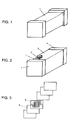
- Fig. 1 is an illustration of the construction of an insulator to be used in an inductance element as a magnetic element in embodiment 1 of the present invention.
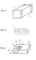
- Fig. 2 is an illustration of the structure of an inductance element that uses the insulator.
- Table 1 shows the composition of examples used in embodiment 1 and composition of magnetic ferrite as control examples.
- the inductance elements as described in embodiment 1 of the present invention have insulator 1 composed of magnetic ferrite having composition shown in Table 1, and conducting coil 2 formed on the surface of insulator 1 and made of copper or silver.
- the inductance elements further have insulating layer 3 made of resin and the like on the surface of conducting coil 2 and external electrodes 4 connected to both ends of conducting coil 2.
- iron oxide powder, zinc oxide powder and cobalt oxide powder as starting materials of magnetic ferrite are compounded at the ratio as shown in Table 1, a proper amount of pure water is added to the compound, the compound is mixed in a ball mill, and mixed powder is obtained by subsequently drying at 120°C.
- Calcined powder of ferrite is obtained by calcining the mixed powder at 900°C and then pulverizing it in a planetary ball mill to a particle size of 8 ⁇ m or smaller.
- Granulating powder having an average particle size of the order of 200 ⁇ m is fabricated by adding a proper amount of a PVA (polyvinyl alcohol) solution to the calcined powder of ferrite, and kneading.
- PVA polyvinyl alcohol
- Insulator 1 is obtained by subsequently filling the granulating powder in a mold, molding under a predetermined molding condition, and firing in a temperature range 1200 to 1300°C, for example, in which the sintered body will become dense.
- Conducting coil 2 is then formed by winding a wire around insulator 1, insulating layer 3 is subsequently formed by using an insulating resin or an insulating inorganic material, and inductance elements as shown in Fig. 2 are obtained (exemplary embodiments 1 to 11).
- inductance element that uses alumina as the material for insulator 1
- inductance element that uses hexagonal ferrite for the material of insulator 1
- Table 1 shows the characteristics of these inductance elements.
- the frequency at which Q value of the inductance element of control example 2 shows a maximum value at around 0.8GHz indicating that the loss at frequencies beyond 1GHz increases so much that the inductance element cannot be used in the GHz band.
- the frequency at which the Q value reaches at a maximum of any of exemplary embodiments 1 to 11 is in the range 2 to 3GHz suggesting that any of these exemplary embodiments can be used in the GHz band.
- the compounding ratio of iron oxide is preferably 50mol% or smaller as the Q value tends to decrease when the compounding ratio is larger than 50mol% when converted to Fe 2 O 3 .
- the compounding ratio of zinc oxide is preferably at least 3mol% as the inductance tends to decrease when the compounding ratio is smaller than 3mol%.
- oxides to be used as the ingredients or sub-components to be used as additives of the composition are oxides or carbonates having different valence such as any of CoO, Co 2 O 3 , Co 3 O 4 , CoCO 3 .
- conducting coil 2 similar advantage is obtainable by forming a spiral coil by forming a film over the entire surface by plating or other thin-film formation technology and spirally cutting it by laser cutting or with a grind stone.
- a magnetic material may be blended in insulating layer 3 thereby to further increase the value of inductance.
- the magnetic material to be blended in insulating layer 3 is preferably powder of magnetic ferrite in accordance with the present invention. Furthermore, it is most preferable that the particle size of the magnetic ferrite powder be 45 ⁇ m or larger as the Q value increases as the particle size increases.
- insulator 1 that uses magnetic ferrite primarily composed of ferric iron, cobalt oxide and zinc oxide as the magnetic core and constructing an inductance element as illustrated in Fig. 1 in this way, an inductance element is realized that can be used in a high frequency range beyond 1GHz.
- a desired value of inductance, an increase in the value of inductance, or miniaturization of an inductance element can be realized.
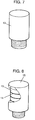
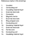
- Fig. 3 and Fig. 4 are illustrations of the structure of an impedance element as a magnetic element in embodiment 2 of the present invention.
- the impedance element in embodiment 2 of the present invention has conductor 5 such as platinum or palladium and magnetic ferrite 6 formed by laminating a green sheet of magnetic ferrite in a manner vertically sandwiching conductor 5. Furthermore, two external electrodes 7 connected to both ends of conductor 5 that is formed in the inside are provided.
- magnetic ferrite 6 is an insulator.
- An impedance element to be used as a noise-reduction component is realized by covering conductor 5, being a signal line, with magnetic ferrite 6.
- the impedance value of the impedance element selectively increases at frequencies beyond the cut-off frequency, and noises having frequency components higher than the cut-off frequency are eliminated.
- Iron oxide, zinc oxide, and cobalt oxide are compounded at the ratios shown in Table 2, a proper amount of pure water is added to the compound, the compound is mixed in a ball mill, and then dried at 120°C to obtain mixed powder.
- Calcined powder of ferrite is obtained by calcining the mixed powder at 900°C and then pulverizing it to a maximum particle size of 8 ⁇ m in a planetary ball mill.
- Ferrite slurry is obtained by adding to this calcined ferrite powder proper amounts of butyral resin and butyl acetate and fully dispersing them in a ball mill.
- ferrite green sheets are obtained from the ferrite slurry thus obtained by means of a doctor blade.
- a pattern of conductor 5 is printed on a ferrite green sheet.
- the ferrite green sheet on which the pattern of conductor 5 has been printed and two or more ferrite green sheets on which no pattern of conductor 5 is printed are laminated to a desirable thickness, followed by cutting to individual pieces to obtain molded chip products.
- Sintered bodies of magnetic ferrite 6 on an inner layer of which conductor 5 has been formed are obtained by firing the molded chip products at 1200 to 1300°C.
- Control example 3 is an impedance element fabricated by using hexagonal ferrite. Table 2 shows electrical characteristics of the impedance elements thus obtained.
- the compounding ratio is preferably 50mol% or smaller. Also, as the impedance value tends to decrease as the compounding ratio of zinc oxide becomes smaller than 3mol%, the compounding ratio of 3mol% or larger is preferable.
- the platinum pattern as conducting coil 5 to be internally formed need not necessarily be a meander shape, and a spiral coil may be formed by laminating a ferrite green sheet through a via hole. In that case, as the impedance value decreases when the spacing between an end portion of spiral conducting coil 5 and external electrodes 7 is short, it is preferable to make the spacing wide. It is most preferable that the spacing be 200 ⁇ m or larger.
- the material for forming conducting coil 5 may be palladium or an alloy of platinum and palladium, platinum or palladium is preferable from the standpoint of obtaining a higher conductivity.
- Fig. 5 and Fig. 6 are illustrations of a common-mode noise filter as an embodiment of a magnetic element of the present invention.
- the common-mode noise filter of embodiment 3 has ring-shaped core 9 made of magnetic ferrite and two conducting coils 10A, 10B formed on the surface of ring-shaped core 9 and made of copper or silver.
- conducting coils 10A, 10B are provided on the surface of conducting coils 10A, 10B and insulating material layer 11 made of resin and the like and four external terminals 12 connected to the terminals of the two conducting coils 10A, 10B.
- Common-mode noise filters used in a differential signaling line of electronic circuits in general are of a structure in which two conducting coils 10A, 10B are wound in the same direction around ring-shaped core 9 made of magnetic ferrite.
- magnetic coupling of the two differential signaling lines can be enhanced by utilizing magnetic permeability ⁇ ' of the magnetic ferrite used and common-mode component can be eliminated.
- the magnetic ferrite of the present invention as ring-shaped core 9 in such a structure, a common-mode noise filter that can be used in GHz band can be realized.
- Ring-shaped core 9 is obtained by forming the granulating powder into a shape of a ring and firing it at 1200 to 1300°C.
- Common-mode noise filters as shown in Fig. 6 are fabricated (exemplary embodiments 23 to 33) by forming on ring-shaped core 9 two conducting coils 10A, 10B by making double windings in the same direction, subsequently forming insulating layer 11 by resin molding, and finally forming external electrodes 12 connected to the terminals of two conducting coils 10A, 10B.
- Control example 4 uses, as the material for ring-shaped core 9, hexagonal ferrite with a compounding ratio as shown in Table 3.
- Table 3 shows characteristics of the common-mode noise filters thus obtained.
- the compounding ratio is preferably 50mol% or smaller. Also, as the coupling coefficient tends to decrease when the compounding ratio of zinc oxide is smaller than 3mol%, the compounding ratio is preferably 3mol% or larger.
- ring-shaped core 9 provided with windings is molded with insulating layer 11 for the ease of surface mounting in this embodiment, similar advantage is obtained when two conducting coils 10A, 10B are directly connected without resin mold.
- Fig. 7 and Fig. 8 are illustrations of an antenna element as a magnetic element of the present invention.
- the antenna element of embodiment 4 has ferrite core 13 made of magnetic ferrite and conducting coil 14 formed on the surface of ferrite core 13 and made of copper or silver. Furthermore, conducting coil 14 has insulating material layer 15 made of resin on its surface.
- granulating powder of calcined ferrite having a compounding ratio as shown in Table 4 is obtained by the same process as embodiment 1. After molding the granulating powder into the shape of a rod, it is fired at 1200 to 1300°C and is then cut to the shape as illustrated in Fig. 7 to obtain ferrite core 13 for an antenna element. Subsequently, a film of a low resistance metal such as copper or silver is formed by plating, for example, over the entire surface of ferrite core 13 followed by spirally cutting the formed metal film to make conducting coil 14.
- a low resistance metal such as copper or silver
- antenna elements of exemplary embodiments 34 to 44 are fabricated by covering ferrite core 13 over which conducting coil 14 has been formed with insulating material layer 15 by resin molding, as shown in Fig.8.
- Control example 5 is an antenna element that uses a resin core of similar configuration
- control example 6 is an antenna element that uses hexagonal ferrite for ferrite core 13.
- Table 4 shows radiation losses of the antenna elements obtained and the size effects of the antenna elements as a percentage relative to the size of an antenna element that uses resin as the core.
- control example 6 shows, the radiation loss of an antenna element that uses hexagonal ferrite as ferrite core 13 is large and the size of the antenna element cannot be precisely determined.
- the compounding ratio of iron oxide 50mol% or smaller when converted to Fe 2 O 3 is preferable because the radiation loss increases when it is larger than 50mol%.
- the compounding ratio of zinc oxide 3mol% or larger is preferable because the advantage of size reduction decreases when it is smaller than 3mol%.
- oxides to be used as the ingredients or sub-components to be used as additives of the composition are oxides or carbonates having different valence such as any of CoO, Co 2 O 3 , Co 3 O 4 , CoCO 3 .
- Connection with a circuit can be made by soldering or caulking, and it is preferable to provide screw threads on the connecting section to secure strength of connection.
- powder press method using a split die may be used in addition to machining.
- Ag, Cu, Au, Al, Ni, Pt, Pd can be used, and Ag and Cu that have large conductivity are more preferable among them.
- a thin film of a nonmagnetic material may be formed between the surface of ferrite core 13 and conducting coil 14.
- the antenna elements may be covered by resin molding or capped with a molded resin case.
- the present invention relates to magnetic elements that employ magnetic ferrite having iron oxide, cobalt oxide and zinc oxide as the main ingredients, and provides magnetic elements that can be used in electronic circuits operable in GHz band.
Landscapes
- Engineering & Computer Science (AREA)
- Chemical & Material Sciences (AREA)
- Ceramic Engineering (AREA)
- Power Engineering (AREA)
- Manufacturing & Machinery (AREA)
- Materials Engineering (AREA)
- Structural Engineering (AREA)
- Organic Chemistry (AREA)
- Microelectronics & Electronic Packaging (AREA)
- Inorganic Chemistry (AREA)
- Coils Or Transformers For Communication (AREA)
- Soft Magnetic Materials (AREA)
- Magnetic Ceramics (AREA)
Applications Claiming Priority (3)
| Application Number | Priority Date | Filing Date | Title |
|---|---|---|---|
| JP2003195044A JP2005032918A (ja) | 2003-07-10 | 2003-07-10 | 磁性素子 |
| JP2003195044 | 2003-07-10 | ||
| PCT/JP2004/009293 WO2005006359A1 (ja) | 2003-07-10 | 2004-06-24 | 磁性素子 |
Publications (2)
| Publication Number | Publication Date |
|---|---|
| EP1548766A1 true EP1548766A1 (de) | 2005-06-29 |
| EP1548766A4 EP1548766A4 (de) | 2011-12-28 |
Family
ID=34055709
Family Applications (1)
| Application Number | Title | Priority Date | Filing Date |
|---|---|---|---|
| EP04746762A Withdrawn EP1548766A4 (de) | 2003-07-10 | 2004-06-24 | Magnetsiches element |
Country Status (5)
| Country | Link |
|---|---|
| US (1) | US7202766B2 (de) |
| EP (1) | EP1548766A4 (de) |
| JP (1) | JP2005032918A (de) |
| CN (1) | CN100543893C (de) |
| WO (1) | WO2005006359A1 (de) |
Families Citing this family (12)
| Publication number | Priority date | Publication date | Assignee | Title |
|---|---|---|---|---|
| JP4736311B2 (ja) * | 2003-07-14 | 2011-07-27 | パナソニック株式会社 | 磁性フェライトおよびそれを用いた磁性素子 |
| US7528795B2 (en) * | 2007-01-09 | 2009-05-05 | Hiercomm, Inc. | High gain antenna and magnetic preamplifier |
| JP4640377B2 (ja) * | 2007-05-30 | 2011-03-02 | Tdk株式会社 | 積層インダクタ部品 |
| TWI399139B (zh) * | 2007-09-19 | 2013-06-11 | Ind Tech Res Inst | 彎繞線狀電感器及具有此彎繞線狀電感器的基板結構 |
| US7671816B2 (en) * | 2007-10-10 | 2010-03-02 | Ethertronics, Inc. | Low frequency antenna |
| JP5374537B2 (ja) * | 2010-05-28 | 2013-12-25 | 住友電気工業株式会社 | 軟磁性粉末、造粒粉、圧粉磁心、電磁部品及び圧粉磁心の製造方法 |
| CN101882503A (zh) * | 2010-06-21 | 2010-11-10 | 贵州航天电器股份有限公司 | 一种耦合变压器 |
| US9728321B2 (en) * | 2015-01-22 | 2017-08-08 | Vladimir Viktorovich KAZAKOV | Transformer with ferromagnetic foil windings |
| KR20160117989A (ko) * | 2015-04-01 | 2016-10-11 | 삼성전기주식회사 | 코일 전자부품 및 그 제조방법 |
| JP6781145B2 (ja) * | 2017-12-28 | 2020-11-04 | 日本発條株式会社 | 携帯型無線通信装置、および携帯型無線通信装置を用いた情報識別装置 |
| US20210118601A1 (en) * | 2019-10-17 | 2021-04-22 | Infineon Technologies Austria Ag | Inductor devices and stacked power supply topologies |
| CN115642032B (zh) * | 2022-12-26 | 2023-09-26 | 兰州大学 | 一种优化Fe-Si软磁复合材料损耗和截止频率磁导率的方法 |
Family Cites Families (18)
| Publication number | Priority date | Publication date | Assignee | Title |
|---|---|---|---|---|
| JPS477821B1 (de) * | 1961-05-13 | 1972-03-06 | ||
| FR1502764A (fr) * | 1966-08-23 | 1967-11-24 | Philips Eclairage Radio | Matériaux ferromagnétiques à base de ferrite de nickel ou de nickel-zinc |
| US4696100A (en) * | 1985-02-21 | 1987-09-29 | Matsushita Electric Industrial Co., Ltd. | Method of manufacturing a chip coil |
| JPH0393667A (ja) * | 1989-09-01 | 1991-04-18 | Hitachi Ferrite Ltd | 高周波用磁性材料 |
| JPH0536517A (ja) | 1991-07-26 | 1993-02-12 | Osamu Kimura | 高周波用磁性材料 |
| US6076253A (en) * | 1994-09-19 | 2000-06-20 | Taiyo Yuden Kabushiki Kaisha | Method of manufacturing chip conductor |
| JPH1126223A (ja) * | 1997-06-30 | 1999-01-29 | Tokin Corp | 複合磁性コア |
| JPH11205017A (ja) * | 1998-01-16 | 1999-07-30 | Yokowo Co Ltd | 携帯無線機用アンテナとその製法およびアンテナの給電構造 |
| JP3752848B2 (ja) * | 1998-05-12 | 2006-03-08 | 株式会社村田製作所 | インダクタ |
| KR100291321B1 (ko) * | 1999-03-26 | 2001-05-15 | 소호연 | 동물훈련장치의 송.수신용 안테나 |
| JP2000348943A (ja) * | 1999-06-02 | 2000-12-15 | Tdk Corp | マルチライン・コモンモードチョークフィルタ |
| JP2000348845A (ja) | 1999-06-04 | 2000-12-15 | Harness Syst Tech Res Ltd | 圧接端子金具の製造方法 |
| EP1324357A4 (de) * | 2000-09-14 | 2008-10-22 | Matsushita Electric Works Ltd | Elektromagnetische einrichtung und hochspannungserzeugungseinrichtung und verfahren zur herstellung der elektromagnetischen einrichtung |
| JP2003031434A (ja) * | 2001-07-13 | 2003-01-31 | Tdk Corp | チップインダクタ部品の製造方法 |
| JP2003059712A (ja) * | 2001-08-10 | 2003-02-28 | Minebea Co Ltd | Mn−Znフェライトおよび巻き線部品 |
| JP2003086425A (ja) * | 2001-09-12 | 2003-03-20 | Fdk Corp | 積層チップインダクタ及びその製造方法 |
| JP4196554B2 (ja) | 2001-09-28 | 2008-12-17 | 三菱マテリアル株式会社 | タグ用アンテナコイル及びそれを用いたrfid用タグ |
| JP3852072B2 (ja) | 2001-09-28 | 2006-11-29 | 株式会社島津製作所 | 油圧サーボ式材料試験機 |
-
2003
- 2003-07-10 JP JP2003195044A patent/JP2005032918A/ja active Pending
-
2004
- 2004-06-24 CN CNB2004800009532A patent/CN100543893C/zh not_active Expired - Fee Related
- 2004-06-24 US US10/529,643 patent/US7202766B2/en not_active Expired - Fee Related
- 2004-06-24 EP EP04746762A patent/EP1548766A4/de not_active Withdrawn
- 2004-06-24 WO PCT/JP2004/009293 patent/WO2005006359A1/ja not_active Ceased
Also Published As
| Publication number | Publication date |
|---|---|
| EP1548766A4 (de) | 2011-12-28 |
| WO2005006359A1 (ja) | 2005-01-20 |
| CN100543893C (zh) | 2009-09-23 |
| US20060066432A1 (en) | 2006-03-30 |
| CN1701400A (zh) | 2005-11-23 |
| JP2005032918A (ja) | 2005-02-03 |
| US7202766B2 (en) | 2007-04-10 |
Similar Documents
| Publication | Publication Date | Title |
|---|---|---|
| KR101210772B1 (ko) | 육방정 페라이트 및 그것을 이용한 안테나 및 통신 기기 | |
| JP3693398B2 (ja) | セラミックス磁性体材料およびこれを用いた高周波用回路部品 | |
| JP2005306696A (ja) | 磁性フェライトおよびそれを用いたコモンモードノイズフィルタ並びにチップトランス | |
| US7589609B2 (en) | Multilayer inductor component | |
| US11626232B2 (en) | Multilayer coil component | |
| US7202766B2 (en) | Magnetic element | |
| US8253643B2 (en) | Chip antenna and its production method, and antenna apparatus and communications apparatus comprising such chip antenna | |
| CN100378028C (zh) | 磁性铁氧体和含有所述铁氧体的磁性装置 | |
| KR100359263B1 (ko) | 자성 세라믹 조성물과 그를 이용한 인덕터 부품 | |
| JP2691715B2 (ja) | フェライト焼結体、チップインダクタおよびlc複合部品 | |
| CN101472855A (zh) | 磁性体天线及铁氧体烧结体 | |
| CN114093588A (zh) | 复合磁性体及电子部件 | |
| JP3320096B2 (ja) | 積層型インダクタおよびその製造方法 | |
| JP4074440B2 (ja) | 磁性酸化物焼結体およびこれを用いた高周波回路部品 | |
| US11996226B2 (en) | Multilayer coil component | |
| JP3337713B2 (ja) | ノイズサブレッサ | |
| KR20010089994A (ko) | 산화물 자성재료, 이 산화물 자성재료를 사용한 칩부품 및산화물 자성재료의 제조방법과 칩부품의 제조방법 | |
| JP4074438B2 (ja) | 磁性酸化物焼結体およびこれを用いた高周波回路部品 | |
| WO2004074208A1 (ja) | 磁性酸化物焼結体およびこれを用いた高周波回路部品 | |
| JP2002280211A (ja) | 酸化物磁性材料とその製造方法および積層チップインダクタ | |
| US20260051435A1 (en) | Laminated coil component | |
| JP2008127222A (ja) | 酸化物磁性材料およびそれを用いたアンテナ素子およびインピーダンス素子 | |
| JP3364267B2 (ja) | チップアンテナ | |
| JP2004143042A (ja) | マイクロ波用磁性体材料とその製造方法およびこれを用いた高周波回路部品 | |
| JP3739977B2 (ja) | 磁性材料とそれを用いたバルク型コイル部品と積層型コイル部品 |
Legal Events
| Date | Code | Title | Description |
|---|---|---|---|
| PUAI | Public reference made under article 153(3) epc to a published international application that has entered the european phase |
Free format text: ORIGINAL CODE: 0009012 |
|
| 17P | Request for examination filed |
Effective date: 20050322 |
|
| AK | Designated contracting states |
Kind code of ref document: A1 Designated state(s): AT BE BG CH CY CZ DE DK EE ES FI FR GB GR HU IE IT LI LU MC NL PL PT RO SE SI SK TR |
|
| AX | Request for extension of the european patent |
Extension state: AL HR LT LV MK |
|
| DAX | Request for extension of the european patent (deleted) | ||
| RBV | Designated contracting states (corrected) |
Designated state(s): DE FR GB |
|
| RAP1 | Party data changed (applicant data changed or rights of an application transferred) |
Owner name: PANASONIC CORPORATION |
|
| A4 | Supplementary search report drawn up and despatched |
Effective date: 20111128 |
|
| RIC1 | Information provided on ipc code assigned before grant |
Ipc: C04B 35/626 20060101ALI20111122BHEP Ipc: C04B 35/26 20060101ALI20111122BHEP Ipc: H01F 17/06 20060101ALI20111122BHEP Ipc: H01F 17/04 20060101ALI20111122BHEP Ipc: H01F 41/04 20060101AFI20111122BHEP |
|
| RAP1 | Party data changed (applicant data changed or rights of an application transferred) |
Owner name: PANASONIC INTELLECTUAL PROPERTY MANAGEMENT CO., LT |
|
| RAP1 | Party data changed (applicant data changed or rights of an application transferred) |
Owner name: PANASONIC INTELLECTUAL PROPERTY MANAGEMENT CO., LT |
|
| STAA | Information on the status of an ep patent application or granted ep patent |
Free format text: STATUS: THE APPLICATION HAS BEEN WITHDRAWN |
|
| 18W | Application withdrawn |
Effective date: 20160210 |