EP1548762A2 - Magnetoresistives element, Magnetkopf, Magnetisches Wiedergabegerät und Magnetischer Speicher - Google Patents
Magnetoresistives element, Magnetkopf, Magnetisches Wiedergabegerät und Magnetischer Speicher Download PDFInfo
- Publication number
- EP1548762A2 EP1548762A2 EP04258000A EP04258000A EP1548762A2 EP 1548762 A2 EP1548762 A2 EP 1548762A2 EP 04258000 A EP04258000 A EP 04258000A EP 04258000 A EP04258000 A EP 04258000A EP 1548762 A2 EP1548762 A2 EP 1548762A2
- Authority
- EP
- European Patent Office
- Prior art keywords
- layer
- nonmagnetic intermediate
- magnetoresistive element
- insulator
- magnetoresistive
- Prior art date
- Legal status (The legal status is an assumption and is not a legal conclusion. Google has not performed a legal analysis and makes no representation as to the accuracy of the status listed.)
- Withdrawn
Links
- 230000005291 magnetic effect Effects 0.000 title claims abstract description 73
- 230000015654 memory Effects 0.000 title claims description 13
- 230000005415 magnetization Effects 0.000 claims abstract description 50
- 239000012212 insulator Substances 0.000 claims abstract description 27
- 239000002184 metal Substances 0.000 claims description 35
- 229910052751 metal Inorganic materials 0.000 claims description 35
- 229910052802 copper Inorganic materials 0.000 claims description 26
- 229910052796 boron Inorganic materials 0.000 claims description 25
- 229910052737 gold Inorganic materials 0.000 claims description 25
- 229910052697 platinum Inorganic materials 0.000 claims description 25
- 229910052702 rhenium Inorganic materials 0.000 claims description 25
- 229910052709 silver Inorganic materials 0.000 claims description 25
- 230000005290 antiferromagnetic effect Effects 0.000 claims description 18
- 239000000956 alloy Substances 0.000 claims description 11
- 229910045601 alloy Inorganic materials 0.000 claims description 11
- 229910052715 tantalum Inorganic materials 0.000 claims description 10
- 229910052782 aluminium Inorganic materials 0.000 claims description 8
- 229910052804 chromium Inorganic materials 0.000 claims description 8
- 229910052750 molybdenum Inorganic materials 0.000 claims description 8
- 229910052758 niobium Inorganic materials 0.000 claims description 8
- 229910052763 palladium Inorganic materials 0.000 claims description 8
- 229910052710 silicon Inorganic materials 0.000 claims description 8
- 229910052719 titanium Inorganic materials 0.000 claims description 8
- 229910052721 tungsten Inorganic materials 0.000 claims description 8
- 229910052720 vanadium Inorganic materials 0.000 claims description 8
- 229910052726 zirconium Inorganic materials 0.000 claims description 8
- 230000000149 penetrating effect Effects 0.000 claims 6
- 239000010410 layer Substances 0.000 description 323
- 239000000463 material Substances 0.000 description 39
- 125000006850 spacer group Chemical group 0.000 description 26
- 239000013078 crystal Substances 0.000 description 23
- 239000010408 film Substances 0.000 description 22
- 230000005294 ferromagnetic effect Effects 0.000 description 18
- 230000000694 effects Effects 0.000 description 17
- 230000001419 dependent effect Effects 0.000 description 14
- 238000010586 diagram Methods 0.000 description 12
- 239000011241 protective layer Substances 0.000 description 12
- 230000008878 coupling Effects 0.000 description 9
- 238000010168 coupling process Methods 0.000 description 9
- 238000005859 coupling reaction Methods 0.000 description 9
- 230000003247 decreasing effect Effects 0.000 description 9
- 229910017107 AlOx Inorganic materials 0.000 description 8
- 230000001747 exhibiting effect Effects 0.000 description 6
- 239000000725 suspension Substances 0.000 description 5
- 229910019041 PtMn Inorganic materials 0.000 description 4
- 230000007423 decrease Effects 0.000 description 4
- 238000002441 X-ray diffraction Methods 0.000 description 3
- 239000000654 additive Substances 0.000 description 3
- 230000000996 additive effect Effects 0.000 description 3
- 230000006399 behavior Effects 0.000 description 3
- 239000011159 matrix material Substances 0.000 description 3
- 239000000203 mixture Substances 0.000 description 3
- 238000001514 detection method Methods 0.000 description 2
- 238000003780 insertion Methods 0.000 description 2
- 230000037431 insertion Effects 0.000 description 2
- 230000015572 biosynthetic process Effects 0.000 description 1
- 230000009977 dual effect Effects 0.000 description 1
- 239000012535 impurity Substances 0.000 description 1
- 230000005381 magnetic domain Effects 0.000 description 1
- 238000000034 method Methods 0.000 description 1
- 229910052707 ruthenium Inorganic materials 0.000 description 1
- 230000035945 sensitivity Effects 0.000 description 1
- 239000000758 substrate Substances 0.000 description 1
- 239000010409 thin film Substances 0.000 description 1
Images


Classifications
-
- H—ELECTRICITY
- H01—ELECTRIC ELEMENTS
- H01F—MAGNETS; INDUCTANCES; TRANSFORMERS; SELECTION OF MATERIALS FOR THEIR MAGNETIC PROPERTIES
- H01F10/00—Thin magnetic films, e.g. of one-domain structure
- H01F10/32—Spin-exchange-coupled multilayers, e.g. nanostructured superlattices
- H01F10/324—Exchange coupling of magnetic film pairs via a very thin non-magnetic spacer, e.g. by exchange with conduction electrons of the spacer
- H01F10/3268—Exchange coupling of magnetic film pairs via a very thin non-magnetic spacer, e.g. by exchange with conduction electrons of the spacer the exchange coupling being asymmetric, e.g. by use of additional pinning, by using antiferromagnetic or ferromagnetic coupling interface, i.e. so-called spin-valve [SV] structure, e.g. NiFe/Cu/NiFe/FeMn
- H01F10/3272—Exchange coupling of magnetic film pairs via a very thin non-magnetic spacer, e.g. by exchange with conduction electrons of the spacer the exchange coupling being asymmetric, e.g. by use of additional pinning, by using antiferromagnetic or ferromagnetic coupling interface, i.e. so-called spin-valve [SV] structure, e.g. NiFe/Cu/NiFe/FeMn by use of anti-parallel coupled [APC] ferromagnetic layers, e.g. artificial ferrimagnets [AFI], artificial [AAF] or synthetic [SAF] anti-ferromagnets
-
- B—PERFORMING OPERATIONS; TRANSPORTING
- B82—NANOTECHNOLOGY
- B82Y—SPECIFIC USES OR APPLICATIONS OF NANOSTRUCTURES; MEASUREMENT OR ANALYSIS OF NANOSTRUCTURES; MANUFACTURE OR TREATMENT OF NANOSTRUCTURES
- B82Y25/00—Nanomagnetism, e.g. magnetoimpedance, anisotropic magnetoresistance, giant magnetoresistance or tunneling magnetoresistance
-
- G—PHYSICS
- G11—INFORMATION STORAGE
- G11B—INFORMATION STORAGE BASED ON RELATIVE MOVEMENT BETWEEN RECORD CARRIER AND TRANSDUCER
- G11B5/00—Recording by magnetisation or demagnetisation of a record carrier; Reproducing by magnetic means; Record carriers therefor
- G11B5/127—Structure or manufacture of heads, e.g. inductive
- G11B5/33—Structure or manufacture of flux-sensitive heads, i.e. for reproduction only; Combination of such heads with means for recording or erasing only
- G11B5/39—Structure or manufacture of flux-sensitive heads, i.e. for reproduction only; Combination of such heads with means for recording or erasing only using magneto-resistive devices or effects
-
- G—PHYSICS
- G11—INFORMATION STORAGE
- G11C—STATIC STORES
- G11C11/00—Digital stores characterised by the use of particular electric or magnetic storage elements; Storage elements therefor
- G11C11/02—Digital stores characterised by the use of particular electric or magnetic storage elements; Storage elements therefor using magnetic elements
- G11C11/16—Digital stores characterised by the use of particular electric or magnetic storage elements; Storage elements therefor using magnetic elements using elements in which the storage effect is based on magnetic spin effect
-
- H—ELECTRICITY
- H01—ELECTRIC ELEMENTS
- H01F—MAGNETS; INDUCTANCES; TRANSFORMERS; SELECTION OF MATERIALS FOR THEIR MAGNETIC PROPERTIES
- H01F10/00—Thin magnetic films, e.g. of one-domain structure
- H01F10/32—Spin-exchange-coupled multilayers, e.g. nanostructured superlattices
- H01F10/324—Exchange coupling of magnetic film pairs via a very thin non-magnetic spacer, e.g. by exchange with conduction electrons of the spacer
- H01F10/3254—Exchange coupling of magnetic film pairs via a very thin non-magnetic spacer, e.g. by exchange with conduction electrons of the spacer the spacer being semiconducting or insulating, e.g. for spin tunnel junction [STJ]
- H01F10/3259—Spin-exchange-coupled multilayers comprising at least a nanooxide layer [NOL], e.g. with a NOL spacer
-
- H—ELECTRICITY
- H01—ELECTRIC ELEMENTS
- H01F—MAGNETS; INDUCTANCES; TRANSFORMERS; SELECTION OF MATERIALS FOR THEIR MAGNETIC PROPERTIES
- H01F10/00—Thin magnetic films, e.g. of one-domain structure
- H01F10/32—Spin-exchange-coupled multilayers, e.g. nanostructured superlattices
- H01F10/324—Exchange coupling of magnetic film pairs via a very thin non-magnetic spacer, e.g. by exchange with conduction electrons of the spacer
- H01F10/3263—Exchange coupling of magnetic film pairs via a very thin non-magnetic spacer, e.g. by exchange with conduction electrons of the spacer the exchange coupling being symmetric, e.g. for dual spin valve, e.g. NiO/Co/Cu/Co/Cu/Co/NiO
-
- H—ELECTRICITY
- H01—ELECTRIC ELEMENTS
- H01F—MAGNETS; INDUCTANCES; TRANSFORMERS; SELECTION OF MATERIALS FOR THEIR MAGNETIC PROPERTIES
- H01F41/00—Apparatus or processes specially adapted for manufacturing or assembling magnets, inductances or transformers; Apparatus or processes specially adapted for manufacturing materials characterised by their magnetic properties
- H01F41/32—Apparatus or processes specially adapted for manufacturing or assembling magnets, inductances or transformers; Apparatus or processes specially adapted for manufacturing materials characterised by their magnetic properties for applying conductive, insulating or magnetic material on a magnetic film, specially adapted for a thin magnetic film
- H01F41/325—Apparatus or processes specially adapted for manufacturing or assembling magnets, inductances or transformers; Apparatus or processes specially adapted for manufacturing materials characterised by their magnetic properties for applying conductive, insulating or magnetic material on a magnetic film, specially adapted for a thin magnetic film applying a noble metal capping on a spin-exchange-coupled multilayer, e.g. spin filter deposition
Definitions
- the present invention relates to a magnetoresistive element, a magnetic head, a magnetic reproducing apparatus, and a magnetic memory, and more particularly to a magnetoresistive element having a structure adapted to flow a sense current in a direction perpendicular to the plane of a magnetoresistive film, and a magnetic head, a magnetic reproducing apparatus, and a magnetic memory using the magnetoresistive element.
- the magnetization of one ferromagnetic layer (referred to as “pinned layer” or “magnetization pinned layer”) is pinned by applying an exchange bias magnetic field, while the magnetization of the other ferromagnetic layer (referred to as “free layer” or “magnetization free layer”) can be reversed by an external magnetic field (for example, signal magnetic field).
- pinned layer or “magnetization pinned layer”
- free layer or “magnetization free layer”
- an external magnetic field for example, signal magnetic field.
- a high magnetoresistive effect can be obtained by changing a relative angle between the magnetization directions of the two ferromagnetic layers having the nonmagnetic layer interposed therebetween.
- the multilayer film of this type is referred to as a "spin-valve".
- the spin-valve can reach magnetization saturation in a low magnetic field, which is suited to an MR head, and has been already put in practical use.
- its magnetoresistive ratio is about 20% at maximum, and therefore a magnetoresistive element with a higher magnetoresistive ratio has been demanded.
- the magnetoresistive element includes two types of structure, that is, a CIP (current-in-plane) type adapted to flow a sense current in a parallel direction to the film plane of the element, and a CPP (current-perpendicular-to-plane) type adapted to flow a sense current in a perpendicular direction to the film plane of the element.
- CIP current-in-plane
- CPP current-perpendicular-to-plane
- the absolute value of the output is as low as about 0.5 m ⁇ ⁇ m 2 for the pinned and free layers having a thickness of 5 nm.
- the spin-valve includes a portion related to spin-dependent scattering of electrons (pinned layer/spacer layer/free layer), and a portion with low spin-dependent scattering (buffer layer, antiferromagnetic layer, protective layer, etc.).
- the resistance adjusting layer includes a portion of an insulator where a current does not flow, and low-resistance portions (metal paths) through which the current flows.
- the current is confined toward the metal paths in the vicinity of the resistance adjusting layer. This is called a current confinement effect. It is only the vicinity of the resistance adjusting layer that the resistance is raised by the current confinement effect, and the spin-dependent scattering at a position remote from the resistance adjusting layer hardly contributes to the MR. Thus, it is effective to arrange a material exhibiting high spin-dependent scattering in the vicinity of the resistance adjusting layer.
- the material is hard to use for a free layer (see Jpn. Pat. Appln. KOKAI Publication No. 2003-60263).
- excellent magnetic characteristics are required for the free layer.
- the free layer is required to have soft magnetic characteristics, such as a low coercivity, and low magnetostriction. These magnetic characteristics depend on the material and crystallinity of the free layer. To satisfy the magnetic characteristics in the material with a high MR, it is important to control the crystallinity of the free layer.
- the resistance adjusting layer inserted in the central portion of the spin-valve, according to the technique disclosed in J. Appl. Phys., 89, p. 6943, 2001 or IEEE Trans. Magn., 38, p. 2277, 2002.
- the insulating portion should be high-quality.
- the resistance adjusting layer is required to have high voltage endurance characteristics.
- the conductive portions should also be high-quality. If the metal paths contain impurities by which electrons with a spin are scattered, the MR will be lowered. Thus, the metal paths should have high purity as possible. What determines the quality of the insulator and metal paths is the grain size and crystal orientation of a portion of the spin-valve located under the resistance adjusting layer. Therefore, it is important to control the grain size and crystal orientation of the layer located under the resistance adjusting layer.
- the spin-valve including the insulator it is important to control the grain size and crystal orientation in order to satisfy both the high MR and magnetic characteristics of the free layer.
- a magnetoresistive element comprises: a magnetoresistive film comprising: a magnetization pinned layer whose magnetization is substantially pinned to one direction; a nonmagnetic intermediate layer formed on the magnetization pinned layer; and a magnetization free layer, formed on the nonmagnetic intermediate layer, whose magnetization is changed in direction depending on an external magnetic field, the magnetization pinned layer or nonmagnetic intermediate layer comprising an insulator; and a pair of electrodes electrically connected to the magnetoresistive film so as to supply a sense current in a direction substantially perpendicular to a plane of the magnetoresistive film, the magnetization free layer comprising a body-centered cubic layer with a body-centered cubic structure, and the thickness of the body-centered cubic layer being 2 nm or more.
- a magnetoresistive element comprises: a magnetoresistive film comprising: a buffer layer; an antiferromagnetic layer formed on the buffer layer; a magnetization pinned layer, formed on the antiferromagnetic layer, whose magnetization is substantially pinned to one direction; a nonmagnetic intermediate layer formed on the magnetization pinned layer; and a magnetization free layer, formed on the nonmagnetic intermediate layer, whose magnetization is changed in direction depending on an external magnetic field, at least one layer of the magnetization pinned layer, nonmagnetic intermediate layer and magnetization free layer comprising an insulator; and a pair of electrodes electrically connected to the magnetoresistive film so as to supply a sense current in a direction substantially perpendicular to a plane of the magnetoresistive film, the buffer layer comprising three types of layers selected from the group consisting of Ta, (Ni 100-x Fe x ) 100-y Cr y alloy (15 ⁇ x ⁇ 25, 20 ⁇ y ⁇ 30), (N
- the word “on” may refer either one or two structural relations between two layers, such as two layers are in contact with each other in a first structural relation, and two layer are not in contact and have other layer(s) between the two layers in a second structural relation.
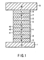
- FIG. 1 is a sectional view of the magnetoresistive element for reference.
- the magnetoresistive element (spin-valve) in FIG. 1 has a stacked structure comprising a lower electrode (LE) 1, a buffer layer (BF) 2, an antiferromagnetic layer (AF) 3, a pinned layer 4 [a first pinned layer (Pl) 41, an anti-parallel coupling layer (AC) 42, and a second pinned layer (P2) 43], a spacer layer (S) 5, a free layer (F) 6, a spin filter layer (SF) 7, a protective layer (PL) 8, and an upper electrode (UE) 9.
- a lower electrode (LE) 1 1, a buffer layer (BF) 2, an antiferromagnetic layer (AF) 3, a pinned layer 4 [a first pinned layer (Pl) 41, an anti-parallel coupling layer (AC) 42, and a second pinned layer (P2) 43], a spacer layer (S) 5, a free layer (F) 6, a spin filter layer (SF) 7, a protective layer (PL) 8, and an upper electrode (UE) 9.
- the first pinned layer 41 has magnetization substantially pinned in one direction by the adjacent antiferromagnetic layer 3, and the second pinned layer 43 has magnetization pinned in the direction opposite to that of the first pinned layer 41 through the anti-parallel coupling layer 42.
- the free layer 6 includes a ferromagnetic layer whose magnetization direction is variable depending on an external magnetic field.
- the spacer layer 5 is a layer interrupting magnetic coupling between the second pinned layer 43 and the free layer 5. In the magnetoresistive element in FIG. 1, the spacer layer 5 is formed of metal only.
- the magnetoresistive element having the structure shown in FIG. 1 was manufactured by use of the following materials.
- the thickness of the first pinned layer 41 was varied depending on the saturation magnetization of the second pinned layer 43.
- the material and thickness of the second pinned layer 43 and free layer 5 were varied as shown in Table 1.
- the magnetoresistance change of the magnetoresistive element and the coercivity Hc of the free layer 5 are also shown in Table 1. Since the entire resistance is low in the spin-valve having no resistance adjusting layer, the output is expressed by the magnetoresistance change (A ⁇ R) per unit area in Table 1 in consideration of ease of understanding.
- the spin valve with 3 nm body-centered cubic materials Fe 50 Co 50 , Fe 80 Co 20 or Fe however, the coercivity of the free layer becomes too large. Therefore, it is necessary to apply the body-centered cubic material with thickness of less than about 3 nm, preferably less than about 2.5 nm.
- a similar tendency is given in other combination of materials.
- a similar tendency as above is confirmed in a free layer formed of a stacked film of a (Fe 100-x Co x ) 100-y Ni y layer (0 ⁇ x ⁇ 85, 0 ⁇ y ⁇ 50) in contact with the spacer and a Ni 100-x Fe x layer (15 ⁇ x ⁇ 25) remote from the spacer.
- an additive element at least one selected from the group consisting of Cu, Au, Ag, Pt, Re and B, referred to as M1 hereinafter
- M1 an additive element
- an M1 metal layer (where M1 is at least one selected from the group consisting of Cu, Au, Ag, Pt, Re and B) with a thickness of one atomic layer or more and 1 nm or less is inserted in the ferromagnetic layer used as the free layer, A ⁇ R can be increased, while the relationship between A ⁇ R and Hc also remains to be in the same tendency as above.
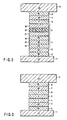
- FIG. 2 is a sectional view showing a magnetoresistive element according to an embodiment of the present invention.
- the magnetoresistive element (spin-valve) in FIG. 2 has a stacked structure comprising a lower electrode (LE) 1, a buffer layer (BF) 2, an antiferromagnetic layer (AF) 3, a pinned layer 4 [a first pinned layer (Pl) 41, an anti-parallel coupling layer (AC) 42, and a second pinned layer (P2) 43], a spacer layer (S) 5 [a first metal layer 51, a resistance increasing layer 52, and a second metal layer 53], a free layer (F) 6, a spin filter layer (SF) 7, a protective layer (PL) 8, and an upper electrode (UE) 9.
- a sense current is applied through the lower electrode 1 and upper electrode 9 in the substantially perpendicular direction to the magnetoresistive film, thus the CPP magnetoresistive element is realized.
- the first pinned layer 41 has magnetization substantially pinned in one direction by the adjacent antiferromagnetic layer 3, and the second pinned layer 43 has magnetisation pinned in the direction opposite to the first pinned layer 41 through the anti-parallel coupling layer 42.
- the free layer 6 includes a ferromagnetic layer whose magnetization direction is variable depending on an external magnetic field.
- the spacer layer 5 is a layer interrupting magnetic coupling between the second pinned layer 93 and the free layer 5.
- the spacer layer 5 has a stacked structure of a first metal layer 51, a resistance increasing layer 52, and a second metal layer 53.
- the resistance increasing layer 52 includes an insulator and metal paths.
- the magnetoresistive element having the structure shown in FIG. 2 was manufactured by use of the following materials.
- the thickness of the first pinned layer 41 was varied depending on the saturation magnetization of the second pinned layer 43.
- the material and thickness of the second pinned layer 43 and free layer 5 were varied as shown in Table 2.
- the spin valve with 3 nm body-centered cubic materials Fe 50 Co 50 , Fe 80 Co 20 or Fe however, the coercivity of the free layer becomes too large. Therefore, it is necessary to apply the body-centered cubic material with thickness of less than about 3 nm, preferably less than about 2.5 nm.
- spin-valve elements having a resistance increasing layer formed in the spacer are described.
- spin-valve elements having a resistance increasing layer formed in the pinned layer can also be manufactured, and it is expected that such spin-valve elements provide the same effects as above.
- a similar tendency is given in other combination of materials.
- a similar tendency as above is confirmed in a free layer formed of a stacked film of a (Fe 100-x Co x ) 100-y Ni y layer (0 ⁇ x ⁇ 85, 0 ⁇ y ⁇ 50) in contact with the spacer and a Ni 100-x Fe x layer (15 ⁇ x ⁇ 25) remote from the spacer.
- it may be effective to use for the free layer an alloy whose composition is slightly adjusted to reduce magnetostriction.
- an additive element at least one selected from the group consisting of Cu, Au, Ag, Pt, Re and B, referred to as M1 hereinafter
- M1 an additive element
- M1 metal layer (where M1 is at least one selected from the group consisting of Cu, Au, Ag, Pt, Re and B) with a thickness of one atomic layer or more and 1 nm or less is inserted in the ferromagnetic layer used as the free layer, MR can be increased, while the relationship between MR and Hc also remains to be in the same tendency as above.
- a higher MR can be obtained by modifying the pinned layer as follows: a (Fe 100-x CO x ) 100-y Ni y layer (0 ⁇ x ⁇ 85, 0 ⁇ y ⁇ 50) serving to exhibit a high MR is used for the pinned layer; an alloy obtained by adding to (Fe 100-x Co x ) 100-y Ni y an additive element M1 (where M1 is at least one selected from the group consisting of Cu, Au, Ag, Pt, Re and B) in the range of more than 0% and less than 10% is used for the pinned layer; and a stacked film having the M1 metal layer (where M1 is at least one selected from the group consisting of Cu, Au, Ag, Pt, Re and B) with a thickness of one atomic layer or more and 1 nm or less is inserted in the ferromagnetic layer is used for the pinned layer.
- the resistance adjusting layer brings about similar effects as above when it includes at least two elements selected from the group consisting of Al, Cr, Mg, Hf, Zr, Si, Ta, Ti, V, Mo, W, Au, Ag, Cu, Pt, Nb, Re, Pd, B and C, and comprises an insulator formed of an oxide of a part of the elements.
- a ferromagnetic layer selected from the following group consisting of (I) to (III) and the grain size thereof is as fine as 7 nm or less on a side in contact with the spacer in the free layer.
- the ferromagnetic layer of (I) to (III) is stacked with a Ni 100-x Fe x layer (15 ⁇ x S 25); a (Ni 100-x Fe x ) 100-z M2 z layer (15 ⁇ x ⁇ 25, 0 ⁇ z ⁇ 10, where M2 is at least one selected from the group consisting of Cu, Au, Ag, Pt, Re and B); or a stacked layer of a Ni 100-x Fe x layer (15 ⁇ x ⁇ 25) and at least one M2 metal layer (where M2 is at least one selected from the group consisting of Cu, Au, Ag, Pt, Re and B) with a thickness of one atomic layer or more and 1 nm or less, Hc is further decreased, but the MR tends to be decreased because the body-centered cubic crystal becomes unstable. To prevent the phenomenon, it is preferable to use a ferromagnetic layer with a Fe-rich composition intrinsically exhibiting a low Hc.
- the body-centered cubic material Fe 100-x Co x ) 100-y Ni y (0 ⁇ x ⁇ 85, 0 ⁇ y ⁇ 50) is added with an element selected from the group consisting of Cu, Au, Ag, Pt, Re and B or stacked with a layer formed of an element selected from the group consisting of Cu, Au, Ag, Pt, Re and B, the Hc can be decreased by about 50% to 70%.
- such materials seem to be appropriate for providing a high MR and a low Hc.
- FIG. 3 is a sectional view of a magnetoresistive element for reference made of only metal layers having no insulating layer.
- the magnetoresistive element (spin-valve) in FIG. 2 has a stacked structure comprising a lower electrode (LE) 1, a buffer layer (BF) 2, an antiferromagnetic layer (AF) 3, a pinned layer (P) 4, a spacer layer (S) 5, a free layer (F) 6, a spin filter layer (SF) 7, a protective layer (PL) 8, and an upper electrode (UE) 9.
- LE lower electrode
- BF buffer layer
- AF antiferromagnetic layer
- P pinned layer
- S spacer layer
- F free layer
- SF spin filter layer
- PL protective layer
- UE upper electrode
- the magnetoresistive element with the structure shown in FIG. 3 was manufactured using the following materials.
- the magnetoresistive elements using these materials for the buffer layer are called 1-A, 1-B, 1-C, and 1-D, respectively.
- the crystal orientation of the magnetoresistive elements using these buffer layers was excellent in the order of 1-B, 1-A, 1-C, and 1-D.
- Each stacked structure was formed on a thermally-oxidized Si substrate, and the relationship between the full width at half maximum (FWHM) of the locking curve by X-ray diffraction of the spin-valve and the resistance change (A ⁇ R) per unit area of element was investigated. The results are shown in FIG. 4.
- the smaller FWHM means the higher crystal orientation. Since the entire resistance of the magnetoresistive element is low relative to the electrode resistance in the case of a magnetoresistive element formed of only metal layers as shown in FIG. 3, comparing the values of A ⁇ R is more precise than comparing the values of MR, and thus the values of A ⁇ R are plotted in FIG. 4. It can be said from FIG. 4 that the crystal orientation does not correlate with the A ⁇ R.
- the grain size also depends largely on the buffer layer. From the sectional TEM observation, it has been found that columnar crystals are grown from the buffer layer to the protective layer. Estimated grain size was about 10 to 15 nm for 1-A and 1-B, and about 30 to 40 nm for 1-C and 1-D.
- FIG. 5 shows the relationship between the grain size and A ⁇ R of the spin-valve element. It can be said from FIG. 5 that the grain size does not correlate with the A ⁇ R.
- the magnetoresistive element having the configuration as shown in FIG. 2 was manufactured by using the following materials.
- FIG. 6A shows the relationship between the thickness of AlO x of the resistance increasing layer and the resistance-area product RA
- FIG. 6B shows the relationship between the thickness of AlO x of the resistance increasing layer and MR.
- the dependence of RA or MR on the AlO x thickness differs with the material of the buffer layer. It is estimated that the crystal orientation and grain size of the magnetoresistive element vary depending on the material of the buffer layer.
- FIG. 7A shows the relationship between the grain size and RA
- FIG. 7B shows the relationship between FWHM and RA
- FIG. 8A shows the relationship between the grain size and MR
- FIG. 8B shows the relationship between FWHM and MR.
- the crystallinity varies between the lower layers under the resistance adjusting layer 52 (layers from the antiferromagnetic layer to the second pinned layer) and the upper layers above the resistance adjusting layer 52 (the free layer and other layers arranged thereon).
- What is related with formation of the resistance adjusting layer 52 is the crystallinity in the portion just under the resistance adjusting layer 52. Thus, it is necessary to observe only the crystallinity of the layer under the resistance adjusting layer 52.
- the orientation determined by the locking curve of X-ray diffraction reflects the orientation of the entire spin-valve film, it is impossible to discriminate between the orientation of the lower layers and that of the upper layers, which are separated by the resistance adjusting film 52. Without the resistance adjusting layer 52, the crystals of the upper layers grow consecutively on the crystals of the lower layers under the spacer. Accordingly, in FIGS. 7B and 8B, the axis of abscissas denotes the FWHM of a model sample using Cu with a thickness of 3 nm as the spacer without inserting the resistance adjusting film.
- the mechanism of such behavior of RA and MR in relation to the grain size may be interpreted as follows.
- the reason why the MR is increased as the grain size becomes smaller is supposed that the metal paths are formed easily and the purity of the metal paths is improved. To the contrary, it is supposed that, when the grain size becomes larger, the metal paths are formed sparsely, which makes the RA somewhat higher, but the current confinement effect is more prominent, which makes the MR higher.
- the behavior of MR in relation to the crystal orientation may be interpreted as follows. Firstly, in the spin-valve of excellent orientation, it is supposed that the quality of the metal paths is improved. Secondly, it is supposed that the interfaces between the first metal layer 51 and the pinned layer and between the second metal layer 53 and the free layer are formed smoothly, which suppresses spin-independent scattering of electrons.
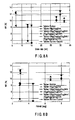
- FIG. 9 shows the relationship between RA and MR.
- the RA of about 500 m ⁇ ⁇ m 2 is required at the areal recording density of 200 Gbpsi.
- the highest MR is obtained in Ta [3 nm] / (Ni 80 Fe 20 ) 60 Cr 50 [5 nm]/(Ni 80 Fe 20 ) 87 Cr 22 [1 nm] with a large grain size and high orientation, and in Ta [5 nm]/Ru [1 nm]/Cu [2 nm] with a small grain size.
- the buffer layer suitable for improving the MR has a grain size of 3 nm to 7 nm, preferably about 5 nm, or a grain size of 25 nm or more, preferably 30 nm or more, and also has an effect of improving crystal orientation.
- the buffer layer is desired to have the lowest layer of Ta, the second layer of (Ni 100-x Fe x ) 100-y Cr y alloy (15 ⁇ x ⁇ 25, 30 ⁇ y ⁇ 45) or Ru, and the third layer of (Ni 100-x Fe x ) 100-y Cr y alloy (15 ⁇ x ⁇ 25, 20 ⁇ y ⁇ 30), Cu or Co 100-x Fe x (5 ⁇ x ⁇ 15).
- Fe 50 Co 50 3 nm and Fe 50 Co 50 1 nm/Ni 80 Fe 20 3.5 nm were used for the materials of the second pinned layer 53 and free layer 6, respectively.
- similar effects as above were obtained by selecting the material of the buffer layer.
- the resistance adjusting layer brings about similar effects as above when it includes at least two elements selected from the group consisting of Al, Cr, Mg, Hf, Zr, Si, Ta, Ti, V, Mo, W, Au, Ag, Cu, Pt, Nb, Re, Pd, B and C, and comprises an insulator formed of an oxide of a part of the elements.
- the resistance increasing layer including the insulator may be inserted also in another layer of the spin-valve, not limited to the spacer. Also in this case, the MR can be increased by using an appropriate buffer layer and controlling the grain size and crystal orientation.
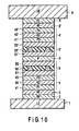
- the magnetoresistive element or magnetic head shown in FIG. 2 or 10 can be assembled, for example, in the magnetic head assembly of integrated type, and can be installed in a magnetic recording/reproducing apparatus.
- FIG. 11 is a perspective view showing a structure of such a magnetic recording/reproducing apparatus.
- the magnetic recording/reproducing apparatus 150 is of a rotary actuator type.
- a recording medium disk 200 is mounted on a spindle 152, and is rotated in direction of the arrow A by a motor (not shown) which responds to control signals from a control unit of a drive controller (not shown).
- the magnetic recording/reproducing apparatus 150 may comprise a plurality of medium disks 200.
- a head slider 153 for writing information to and reading information from the medium disk 200 is mounted on the distal end of a suspension 154.
- the head slider 153 has the magnetoresistive element or magnetic head of any type of the embodiments formed thereon.
- the air-bearing surface (ABS) of the header slider 153 is held at a predetermined flying height from the surface of the medium disk 200.
- the slider may be in contact with the medium disk 200, which is known as "contact type".
- the suspension 154 is connected to one end of an actuator arm 155 having a bobbin for holding a driving coil (not shown).
- a voice coil motor 156 which is a type of linear motor is disposed.
- the voice coil motor 156 is composed of a driving coil (not shown) wound around the bobbin of the actuator arm 155, and a magnetic circuit including a permanent magnet and an opposite yoke disposed to sandwich the coil.
- the actuator arm 155 is held by two ball bearings (not shown) disposed at upper and lower positions of a pivot 157, and is free to rotate and slide by means of the voice coil motor 156.
- FIG. 12 is a magnified perspective view of the distal end of the magnetic head assembly including the actuator arm 155 viewed from the disk side. That is, the magnetic head assembly 160, for example, has the actuator arm 155 having the bobbin for holding the driving coil, and the suspension 154 is connected to one end of the actuator arm 155.
- the head slider 153 having the magnetoresistive element or magnetic head shown in FIG. 2 or 10 is mounted.
- the suspension 154 has lead wires 164 for writing and reading signals, and the lead wires 164 are electrically connected to electrodes of the magnetic head assembled in the head slider 153.
- Reference numeral 165 in the figure represents electrode pads of the magnetic head assembly 160.
- a magnetic memory having a magnetoresistive element according to an embodiment of the present invention mounted thereon will be described.
- a magnetic memory such as magnetic random access memory having memory cells arrayed in matrix can be realized.
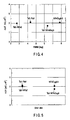
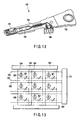
- FIG. 13 is a diagram showing an example of a matrix structure of the magnetic memory according to an embodiment of the present invention.
- the diagram shows a circuit configuration of the embodiment in which memory cells are arrayed.
- a row decoder 350 and a line decoder 351 are provided to select one bit in the array.
- a switching transistor 330 is selected and turned on by a bit line 334 and a word line 332, and bit information recorded in the magnetic recording layer included in a magnetoresistive element 321 can be read out through detection by a sense amplifier 352,.
- write current is applied in specified word line 323 and bit line 322 to generate a magnetic field.
- the magnetic memory according to the embodiment of the present invention provides a high negative magnetoresistive effect by using the magnetoresistive element shown in FIG. 2 or 10. Therefore, the magnetic domains of the recording layer can be securely controlled if the cell size is reduced, and reliable writing is assured, and reading is also realised securely.
- the detection resolution of the magnetic head can be defined by forming magnetic shields above and beneath the element.
- the present invention can be also applied in the magnetic head or magnetic reproducing apparatus of a longitudinal magnetic recording system or a perpendicular magnetic recording system, and the same effects can be obtained.
- the magnetic reproducing apparatus of the present invention may be either rigid type having a specific rigid recording medium, or removable type having an removable recording medium.
Landscapes
- Engineering & Computer Science (AREA)
- Chemical & Material Sciences (AREA)
- Crystallography & Structural Chemistry (AREA)
- Nanotechnology (AREA)
- Manufacturing & Machinery (AREA)
- Computer Hardware Design (AREA)
- Power Engineering (AREA)
- Hall/Mr Elements (AREA)
- Magnetic Heads (AREA)
- Mram Or Spin Memory Techniques (AREA)
- Thin Magnetic Films (AREA)
- Semiconductor Memories (AREA)
Applications Claiming Priority (2)
| Application Number | Priority Date | Filing Date | Title |
|---|---|---|---|
| JP2003431571A JP4776164B2 (ja) | 2003-12-25 | 2003-12-25 | 磁気抵抗効果素子、磁気ヘッド、磁気再生装置および磁気メモリ |
| JP2003431571 | 2003-12-25 |
Publications (2)
| Publication Number | Publication Date |
|---|---|
| EP1548762A2 true EP1548762A2 (de) | 2005-06-29 |
| EP1548762A3 EP1548762A3 (de) | 2010-02-17 |
Family
ID=34545052
Family Applications (1)
| Application Number | Title | Priority Date | Filing Date |
|---|---|---|---|
| EP04258000A Withdrawn EP1548762A3 (de) | 2003-12-25 | 2004-12-21 | Magnetoresistives element, Magnetkopf, Magnetisches Wiedergabegerät und Magnetischer Speicher |
Country Status (4)
| Country | Link |
|---|---|
| US (1) | US7426098B2 (de) |
| EP (1) | EP1548762A3 (de) |
| JP (1) | JP4776164B2 (de) |
| CN (1) | CN100347748C (de) |
Cited By (11)
| Publication number | Priority date | Publication date | Assignee | Title |
|---|---|---|---|---|
| WO2007072987A1 (en) * | 2005-12-21 | 2007-06-28 | Kabushiki Kaisha Toshiba | Magnetoresistive effect element and manufacturing method thereof |
| US7897201B2 (en) | 2006-02-09 | 2011-03-01 | Kabushiki Kaisha Toshiba | Method for manufacturing magnetoresistance effect element |
| US20110205669A1 (en) * | 2010-02-22 | 2011-08-25 | Kabushiki Kaisha Toshiba | Method for manufacturing magneto-resistance effect element, magnetic head assembly, and magnetic recording and reproducing apparatus |
| US8031443B2 (en) | 2007-03-27 | 2011-10-04 | Kabushiki Kaisha Toshiba | Magneto-resistance effect element, magnetic head, magnetic recording/reproducing device and method for manufacturing a magneto-resistance effect element |
| US8111489B2 (en) | 2006-07-07 | 2012-02-07 | Kabushiki Kaisha Toshiba | Magneto-resistance effect element |
| US8228643B2 (en) | 2008-09-26 | 2012-07-24 | Kabushiki Kaisha Toshiba | Method for manufacturing a magneto-resistance effect element and magnetic recording and reproducing apparatus |
| US8274766B2 (en) | 2006-04-28 | 2012-09-25 | Kabushiki Kaisha Toshiba | Magnetic recording element including a thin film layer with changeable magnetization direction |
| US8274765B2 (en) | 2008-09-29 | 2012-09-25 | Kabushiki Kaisha Toshiba | Method of manufacturing magnetoresistive element, magnetoresistive element, magnetic head assembly and magnetic recording apparatus |
| US8305716B2 (en) | 2005-09-29 | 2012-11-06 | Kabushiki Kaisha Toshiba | Magneto-resistance effect element including diffusive electron scattering layer, magneto-resistance effect head, magnetic storage and magnetic memory |
| US8315020B2 (en) | 2008-09-26 | 2012-11-20 | Kabushiki Kaisha Toshiba | Method for manufacturing a magneto-resistance effect element and magnetic recording and reproducing apparatus |
| US8917485B2 (en) | 2006-03-27 | 2014-12-23 | Kabushiki Kaisha Toshiba | Magnetoresistive effect element, magnetic head, and magnetic disk apparatus |
Families Citing this family (29)
| Publication number | Priority date | Publication date | Assignee | Title |
|---|---|---|---|---|
| JP4024499B2 (ja) * | 2001-08-15 | 2007-12-19 | 株式会社東芝 | 磁気抵抗効果素子、磁気ヘッド及び磁気再生装置 |
| US7323215B2 (en) * | 2004-05-14 | 2008-01-29 | Headway Technologies, Inc. | Free layer design for CPP GMR enhancement |
| JP2006114610A (ja) * | 2004-10-13 | 2006-04-27 | Toshiba Corp | 磁気抵抗効果素子とそれを用いた磁気ヘッドおよび磁気再生装置 |
| JP4261454B2 (ja) * | 2004-10-13 | 2009-04-30 | 株式会社東芝 | 磁気抵抗効果素子とそれを用いた磁気ヘッドおよび磁気再生装置 |
| JP5095076B2 (ja) * | 2004-11-09 | 2012-12-12 | 株式会社東芝 | 磁気抵抗効果素子 |
| JP2006351919A (ja) * | 2005-06-17 | 2006-12-28 | Alps Electric Co Ltd | 磁気検出素子 |
| JP4705478B2 (ja) * | 2006-01-19 | 2011-06-22 | ヒタチグローバルストレージテクノロジーズネザーランドビーブイ | 磁気ヘッド |
| WO2007086325A1 (ja) * | 2006-01-24 | 2007-08-02 | Matsushita Electric Industrial Co., Ltd. | 電気素子,メモリ装置,および半導体集積回路 |
| US7610674B2 (en) * | 2006-02-13 | 2009-11-03 | Headway Technologies, Inc. | Method to form a current confining path of a CPP GMR device |
| JP4975335B2 (ja) * | 2006-02-16 | 2012-07-11 | 株式会社東芝 | 磁気抵抗効果素子,磁気ヘッド,および磁気記録再生装置 |
| JP2007273561A (ja) * | 2006-03-30 | 2007-10-18 | Toshiba Corp | 磁気抵抗効果素子、磁気ヘッドおよび磁気再生装置 |
| JP2007273504A (ja) * | 2006-03-30 | 2007-10-18 | Fujitsu Ltd | 磁気抵抗効果素子、磁気ヘッド、磁気記録装置、磁気ランダムアクセスメモリ |
| JP4834834B2 (ja) * | 2006-05-08 | 2011-12-14 | 国立大学法人東北大学 | トンネル磁気抵抗素子、不揮発性磁気メモリ、発光素子および3端子素子 |
| JP2008041827A (ja) | 2006-08-03 | 2008-02-21 | Alps Electric Co Ltd | トンネル型磁気検出素子及びその製造方法 |
| JP4862564B2 (ja) | 2006-08-30 | 2012-01-25 | Tdk株式会社 | トンネル型磁気検出素子およびその製造方法 |
| JP4764294B2 (ja) * | 2006-09-08 | 2011-08-31 | 株式会社東芝 | 磁気抵抗効果素子、及び磁気ヘッド |
| JP2008071868A (ja) * | 2006-09-13 | 2008-03-27 | Alps Electric Co Ltd | トンネル型磁気検出素子およびその製造方法 |
| US8068315B2 (en) * | 2007-09-26 | 2011-11-29 | Hitachi Global Storage Technologies Netherlands B.V. | Current perpendicular to plane GMR and TMR sensors with improved magnetic properties using Ru/Si seed layers |
| JP4557037B2 (ja) * | 2008-04-08 | 2010-10-06 | ウシオ電機株式会社 | Led光放射装置 |
| JP5032429B2 (ja) * | 2008-09-26 | 2012-09-26 | 株式会社東芝 | 磁気抵抗効果素子の製造方法、磁気抵抗効果素子、磁気ヘッドアセンブリ及び磁気記録再生装置 |
| JP5032430B2 (ja) * | 2008-09-26 | 2012-09-26 | 株式会社東芝 | 磁気抵抗効果素子の製造方法、磁気抵抗効果素子、磁気ヘッドアセンブリ及び磁気記録再生装置 |
| JP5118766B2 (ja) * | 2011-08-24 | 2013-01-16 | 株式会社東芝 | 磁気抵抗効果素子、磁気抵抗効果ヘッド、磁気記憶装置、および磁気メモリ |
| JP5197826B2 (ja) * | 2011-10-27 | 2013-05-15 | 株式会社東芝 | 磁気抵抗効果素子、磁気抵抗効果ヘッド、磁気記憶装置、および磁気メモリ |
| ITTO20120614A1 (it) * | 2012-07-11 | 2014-01-12 | St Microelectronics Srl | Sensore magnetoresistivo integrato multistrato e relativo metodo di fabbricazione |
| JP2013016820A (ja) * | 2012-08-20 | 2013-01-24 | Hitachi Ltd | トンネル磁気抵抗効果素子、それを用いた磁気メモリセル及びランダムアクセスメモリ |
| JP5814898B2 (ja) * | 2012-10-17 | 2015-11-17 | 株式会社東芝 | 磁気抵抗効果素子、およびその製造方法 |
| JP6054479B2 (ja) * | 2015-06-30 | 2016-12-27 | 株式会社東芝 | 磁気抵抗効果素子、磁気ヘッド、磁気記録再生装置、磁気メモリ、磁界センサ |
| US11730063B2 (en) * | 2019-12-17 | 2023-08-15 | Tdk Corporation | Magnetoresistive effect element including a Heusler alloy layer with a crystal region and an amorphous region |
| WO2022209548A1 (ja) * | 2021-03-30 | 2022-10-06 | 株式会社村田製作所 | 磁気センサ |
Family Cites Families (23)
| Publication number | Priority date | Publication date | Assignee | Title |
|---|---|---|---|---|
| US5608593A (en) * | 1995-03-09 | 1997-03-04 | Quantum Peripherals Colorado, Inc. | Shaped spin valve type magnetoresistive transducer and method for fabricating the same incorporating domain stabilization technique |
| US6080445A (en) * | 1997-02-20 | 2000-06-27 | Citizen Watch Co., Ltd. | Method of forming films over insulating material |
| JPH1186229A (ja) | 1997-09-16 | 1999-03-30 | Hitachi Metals Ltd | スピンバルブ効果センサ |
| US6313973B1 (en) * | 1998-06-30 | 2001-11-06 | Kabushiki Kaisha Toshiba | Laminated magnetorestrictive element of an exchange coupling film, an antiferromagnetic film and a ferromagnetic film and a magnetic disk drive using same |
| US6411476B1 (en) * | 1999-10-28 | 2002-06-25 | International Business Machines Corporation | Trilayer seed layer structure for spin valve sensor |
| US6452763B1 (en) * | 2000-06-06 | 2002-09-17 | International Business Machines Corporation | GMR design with nano oxide layer in the second anti-parallel pinned layer |
| US6521098B1 (en) * | 2000-08-31 | 2003-02-18 | International Business Machines Corporation | Fabrication method for spin valve sensor with insulating and conducting seed layers |
| JP3618654B2 (ja) | 2000-09-11 | 2005-02-09 | 株式会社東芝 | 磁気抵抗効果素子、磁気ヘッド及び磁気記録再生装置 |
| JP3833512B2 (ja) * | 2000-10-20 | 2006-10-11 | 株式会社東芝 | 磁気抵抗効果素子 |
| US6937446B2 (en) * | 2000-10-20 | 2005-08-30 | Kabushiki Kaisha Toshiba | Magnetoresistance effect element, magnetic head and magnetic recording and/or reproducing system |
| JP4167428B2 (ja) * | 2001-02-01 | 2008-10-15 | 株式会社東芝 | 磁気抵抗効果素子、磁気抵抗効果ヘッド、および磁気記録再生装置 |
| US6905780B2 (en) * | 2001-02-01 | 2005-06-14 | Kabushiki Kaisha Toshiba | Current-perpendicular-to-plane-type magnetoresistive device, and magnetic head and magnetic recording-reproducing apparatus using the same |
| JP4050481B2 (ja) * | 2001-04-17 | 2008-02-20 | ジーイー・メディカル・システムズ・グローバル・テクノロジー・カンパニー・エルエルシー | 超音波撮影装置 |
| JP3565268B2 (ja) * | 2001-06-22 | 2004-09-15 | 株式会社東芝 | 磁気抵抗効果素子、磁気ヘッド及び磁気再生装置 |
| JP2003016613A (ja) * | 2001-06-28 | 2003-01-17 | Hitachi Ltd | 磁気ヘッド |
| JP4024499B2 (ja) | 2001-08-15 | 2007-12-19 | 株式会社東芝 | 磁気抵抗効果素子、磁気ヘッド及び磁気再生装置 |
| JP4184668B2 (ja) | 2002-01-10 | 2008-11-19 | 富士通株式会社 | Cpp構造磁気抵抗効果素子 |
| JP3749873B2 (ja) | 2002-03-28 | 2006-03-01 | 株式会社東芝 | 磁気抵抗効果素子、磁気ヘッド及び磁気再生装置 |
| US6785103B2 (en) * | 2002-04-12 | 2004-08-31 | International Business Machines Corporation | Magnetoresistance sensor with reduced side reading |
| JP3648504B2 (ja) * | 2002-09-06 | 2005-05-18 | 株式会社東芝 | 磁気抵抗効果素子、磁気ヘッドおよび磁気再生装置 |
| US6961224B2 (en) * | 2003-09-24 | 2005-11-01 | Hitachi Global Storage Technologies Netherlands, B.V. | GMR enhancing seed layer for self pinned spin valves |
| US7180714B2 (en) * | 2003-09-30 | 2007-02-20 | Hitachi Global Storage Technolgies Netherlands B.V. | Apparatus for providing a ballistic magnetoresistive sensor in a current perpendicular-to-plane mode |
| US7221545B2 (en) * | 2004-02-18 | 2007-05-22 | Hitachi Global Storage Technologies Netherlands B.V. | High HC reference layer structure for self-pinned GMR heads |
-
2003
- 2003-12-25 JP JP2003431571A patent/JP4776164B2/ja not_active Expired - Fee Related
-
2004
- 2004-12-21 EP EP04258000A patent/EP1548762A3/de not_active Withdrawn
- 2004-12-22 US US11/017,965 patent/US7426098B2/en not_active Expired - Lifetime
- 2004-12-24 CN CNB2004100941603A patent/CN100347748C/zh not_active Expired - Fee Related
Cited By (12)
| Publication number | Priority date | Publication date | Assignee | Title |
|---|---|---|---|---|
| US8305716B2 (en) | 2005-09-29 | 2012-11-06 | Kabushiki Kaisha Toshiba | Magneto-resistance effect element including diffusive electron scattering layer, magneto-resistance effect head, magnetic storage and magnetic memory |
| WO2007072987A1 (en) * | 2005-12-21 | 2007-06-28 | Kabushiki Kaisha Toshiba | Magnetoresistive effect element and manufacturing method thereof |
| US8048492B2 (en) | 2005-12-21 | 2011-11-01 | Kabushiki Kaisha Toshiba | Magnetoresistive effect element and manufacturing method thereof |
| US7897201B2 (en) | 2006-02-09 | 2011-03-01 | Kabushiki Kaisha Toshiba | Method for manufacturing magnetoresistance effect element |
| US8917485B2 (en) | 2006-03-27 | 2014-12-23 | Kabushiki Kaisha Toshiba | Magnetoresistive effect element, magnetic head, and magnetic disk apparatus |
| US8274766B2 (en) | 2006-04-28 | 2012-09-25 | Kabushiki Kaisha Toshiba | Magnetic recording element including a thin film layer with changeable magnetization direction |
| US8111489B2 (en) | 2006-07-07 | 2012-02-07 | Kabushiki Kaisha Toshiba | Magneto-resistance effect element |
| US8031443B2 (en) | 2007-03-27 | 2011-10-04 | Kabushiki Kaisha Toshiba | Magneto-resistance effect element, magnetic head, magnetic recording/reproducing device and method for manufacturing a magneto-resistance effect element |
| US8228643B2 (en) | 2008-09-26 | 2012-07-24 | Kabushiki Kaisha Toshiba | Method for manufacturing a magneto-resistance effect element and magnetic recording and reproducing apparatus |
| US8315020B2 (en) | 2008-09-26 | 2012-11-20 | Kabushiki Kaisha Toshiba | Method for manufacturing a magneto-resistance effect element and magnetic recording and reproducing apparatus |
| US8274765B2 (en) | 2008-09-29 | 2012-09-25 | Kabushiki Kaisha Toshiba | Method of manufacturing magnetoresistive element, magnetoresistive element, magnetic head assembly and magnetic recording apparatus |
| US20110205669A1 (en) * | 2010-02-22 | 2011-08-25 | Kabushiki Kaisha Toshiba | Method for manufacturing magneto-resistance effect element, magnetic head assembly, and magnetic recording and reproducing apparatus |
Also Published As
| Publication number | Publication date |
|---|---|
| CN100347748C (zh) | 2007-11-07 |
| EP1548762A3 (de) | 2010-02-17 |
| JP2005191312A (ja) | 2005-07-14 |
| CN1637859A (zh) | 2005-07-13 |
| US20050168887A1 (en) | 2005-08-04 |
| JP4776164B2 (ja) | 2011-09-21 |
| US7426098B2 (en) | 2008-09-16 |
Similar Documents
| Publication | Publication Date | Title |
|---|---|---|
| US7426098B2 (en) | Magnetoresistive element having three-layer buffer layer, magnetic head, magnetic reproducing apparatus, and magnetic memory | |
| CN100382353C (zh) | 磁电阻效应元件、磁头和磁再现设备 | |
| US6905780B2 (en) | Current-perpendicular-to-plane-type magnetoresistive device, and magnetic head and magnetic recording-reproducing apparatus using the same | |
| CN100446086C (zh) | 磁致电阻元件、磁头、磁记录装置以及磁存储器 | |
| CN100380448C (zh) | 磁阻效应元件、磁头和磁存储装置 | |
| US6816347B2 (en) | Magnetoresistive element and magnetic recording apparatus | |
| US7196877B2 (en) | Magnetoresistive element, magnetoresistive head and magnetic reproducing apparatus | |
| US7525776B2 (en) | Magnetoresistive element, magnetoresistive head, magnetic recording apparatus, and magnetic memory | |
| US6917088B2 (en) | Magneto-resistive devices | |
| US7742262B2 (en) | Magnetoresistive element, magnetic head, magnetic recording apparatus, and magnetic memory | |
| US7289305B2 (en) | Magnetoresistive element, magnetic head, and magnetic recording and reproducing apparatus | |
| CN101276878A (zh) | 磁阻效应元件及其制造方法 | |
| US7602592B2 (en) | Magnetoresistive element including connection layers with magnetization alignment angles therebetween of 30 to 60° between metallic magnetic layers | |
| JP2007273504A (ja) | 磁気抵抗効果素子、磁気ヘッド、磁気記録装置、磁気ランダムアクセスメモリ | |
| JP2012178442A (ja) | 磁気抵抗効果素子、磁気ヘッドアセンブリ、磁気記録再生装置、メモリセルアレイ、及び磁気抵抗効果素子の製造方法 | |
| JP2004047583A (ja) | 磁気抵抗効果素子とこれを用いた磁気ヘッドおよび磁気メモリならびに磁気記録装置 | |
| JP2008016738A (ja) | 磁気抵抗効果素子、磁気ヘッド、磁気記録再生装置、および磁気メモリ | |
| JP2007250756A (ja) | 磁気抵抗効果素子及び強磁性構造の製造方法 | |
| JP2001052314A (ja) | 磁気抵抗効果素子 |
Legal Events
| Date | Code | Title | Description |
|---|---|---|---|
| PUAI | Public reference made under article 153(3) epc to a published international application that has entered the european phase |
Free format text: ORIGINAL CODE: 0009012 |
|
| 17P | Request for examination filed |
Effective date: 20050121 |
|
| AK | Designated contracting states |
Kind code of ref document: A2 Designated state(s): AT BE BG CH CY CZ DE DK EE ES FI FR GB GR HU IE IS IT LI LT LU MC NL PL PT RO SE SI SK TR |
|
| AX | Request for extension of the european patent |
Extension state: AL BA HR LV MK YU |
|
| PUAL | Search report despatched |
Free format text: ORIGINAL CODE: 0009013 |
|
| AK | Designated contracting states |
Kind code of ref document: A3 Designated state(s): AT BE BG CH CY CZ DE DK EE ES FI FR GB GR HU IE IS IT LI LT LU MC NL PL PT RO SE SI SK TR |
|
| AX | Request for extension of the european patent |
Extension state: AL BA HR LV MK YU |
|
| AKX | Designation fees paid |
Designated state(s): DE FR GB |
|
| STAA | Information on the status of an ep patent application or granted ep patent |
Free format text: STATUS: THE APPLICATION IS DEEMED TO BE WITHDRAWN |
|
| 18D | Application deemed to be withdrawn |
Effective date: 20100701 |