EP1548502A1 - Lithographischer Apparat und Verfahren zur Herstellung einer Vorrichtung - Google Patents
Lithographischer Apparat und Verfahren zur Herstellung einer Vorrichtung Download PDFInfo
- Publication number
- EP1548502A1 EP1548502A1 EP04078274A EP04078274A EP1548502A1 EP 1548502 A1 EP1548502 A1 EP 1548502A1 EP 04078274 A EP04078274 A EP 04078274A EP 04078274 A EP04078274 A EP 04078274A EP 1548502 A1 EP1548502 A1 EP 1548502A1
- Authority
- EP
- European Patent Office
- Prior art keywords
- article
- backfill gas
- substrate
- pressure
- article support
- Prior art date
- Legal status (The legal status is an assumption and is not a legal conclusion. Google has not performed a legal analysis and makes no representation as to the accuracy of the status listed.)
- Withdrawn
Links
Images


Classifications
-
- H—ELECTRICITY
- H01—ELECTRIC ELEMENTS
- H01L—SEMICONDUCTOR DEVICES NOT COVERED BY CLASS H10
- H01L21/00—Processes or apparatus adapted for the manufacture or treatment of semiconductor or solid state devices or of parts thereof
- H01L21/67—Apparatus specially adapted for handling semiconductor or electric solid state devices during manufacture or treatment thereof; Apparatus specially adapted for handling wafers during manufacture or treatment of semiconductor or electric solid state devices or components ; Apparatus not specifically provided for elsewhere
- H01L21/683—Apparatus specially adapted for handling semiconductor or electric solid state devices during manufacture or treatment thereof; Apparatus specially adapted for handling wafers during manufacture or treatment of semiconductor or electric solid state devices or components ; Apparatus not specifically provided for elsewhere for supporting or gripping
- H01L21/6831—Apparatus specially adapted for handling semiconductor or electric solid state devices during manufacture or treatment thereof; Apparatus specially adapted for handling wafers during manufacture or treatment of semiconductor or electric solid state devices or components ; Apparatus not specifically provided for elsewhere for supporting or gripping using electrostatic chucks
-
- G—PHYSICS
- G03—PHOTOGRAPHY; CINEMATOGRAPHY; ANALOGOUS TECHNIQUES USING WAVES OTHER THAN OPTICAL WAVES; ELECTROGRAPHY; HOLOGRAPHY
- G03F—PHOTOMECHANICAL PRODUCTION OF TEXTURED OR PATTERNED SURFACES, e.g. FOR PRINTING, FOR PROCESSING OF SEMICONDUCTOR DEVICES; MATERIALS THEREFOR; ORIGINALS THEREFOR; APPARATUS SPECIALLY ADAPTED THEREFOR
- G03F7/00—Photomechanical, e.g. photolithographic, production of textured or patterned surfaces, e.g. printing surfaces; Materials therefor, e.g. comprising photoresists; Apparatus specially adapted therefor
- G03F7/70—Microphotolithographic exposure; Apparatus therefor
- G03F7/70691—Handling of masks or workpieces
- G03F7/707—Chucks, e.g. chucking or un-chucking operations or structural details
- G03F7/70708—Chucks, e.g. chucking or un-chucking operations or structural details being electrostatic; Electrostatically deformable vacuum chucks
-
- G—PHYSICS
- G03—PHOTOGRAPHY; CINEMATOGRAPHY; ANALOGOUS TECHNIQUES USING WAVES OTHER THAN OPTICAL WAVES; ELECTROGRAPHY; HOLOGRAPHY
- G03F—PHOTOMECHANICAL PRODUCTION OF TEXTURED OR PATTERNED SURFACES, e.g. FOR PRINTING, FOR PROCESSING OF SEMICONDUCTOR DEVICES; MATERIALS THEREFOR; ORIGINALS THEREFOR; APPARATUS SPECIALLY ADAPTED THEREFOR
- G03F7/00—Photomechanical, e.g. photolithographic, production of textured or patterned surfaces, e.g. printing surfaces; Materials therefor, e.g. comprising photoresists; Apparatus specially adapted therefor
- G03F7/70—Microphotolithographic exposure; Apparatus therefor
- G03F7/708—Construction of apparatus, e.g. environment aspects, hygiene aspects or materials
- G03F7/70858—Environment aspects, e.g. pressure of beam-path gas, temperature
- G03F7/70866—Environment aspects, e.g. pressure of beam-path gas, temperature of mask or workpiece
- G03F7/70875—Temperature, e.g. temperature control of masks or workpieces via control of stage temperature
-
- H—ELECTRICITY
- H01—ELECTRIC ELEMENTS
- H01L—SEMICONDUCTOR DEVICES NOT COVERED BY CLASS H10
- H01L21/00—Processes or apparatus adapted for the manufacture or treatment of semiconductor or solid state devices or of parts thereof
- H01L21/67—Apparatus specially adapted for handling semiconductor or electric solid state devices during manufacture or treatment thereof; Apparatus specially adapted for handling wafers during manufacture or treatment of semiconductor or electric solid state devices or components ; Apparatus not specifically provided for elsewhere
- H01L21/683—Apparatus specially adapted for handling semiconductor or electric solid state devices during manufacture or treatment thereof; Apparatus specially adapted for handling wafers during manufacture or treatment of semiconductor or electric solid state devices or components ; Apparatus not specifically provided for elsewhere for supporting or gripping
- H01L21/687—Apparatus specially adapted for handling semiconductor or electric solid state devices during manufacture or treatment thereof; Apparatus specially adapted for handling wafers during manufacture or treatment of semiconductor or electric solid state devices or components ; Apparatus not specifically provided for elsewhere for supporting or gripping using mechanical means, e.g. chucks, clamps or pinches
Definitions
- the present invention relates to a lithographic apparatus and a device manufacturing method.
- a lithographic apparatus is a machine that applies a desired pattern onto a target portion of a substrate.
- Lithographic apparatus can be used, for example, in the manufacture of integrated circuits (ICs).
- a patterning device such as a mask, may be used to generate a circuit pattern corresponding to an individual layer of the IC, and this pattern can be imaged onto a target portion (e.g. comprising part of, one or several dies) on a substrate (e.g. a silicon wafer) that has a layer of radiation-sensitive material (resist).
- a single substrate will contain a network of adjacent target portions that are successively exposed.
- lithographic apparatus include so-called steppers, in which each target portion is irradiated by exposing an entire pattern onto the target portion in one go, and so-called scanners, in which each target portion is irradiated by scanning the pattern through the projection beam in a given direction (the "scanning"-direction) while synchronously scanning the substrate parallel or anti-parallel to this direction.
- an article such as a wafer or reticle is clamped on an article support by a clamping force, that may range from vacuum pressure forces, electrostatic forces, intermolecular binding forces or just gravity force.
- the article support defines a plane, in the form of a plurality of protrusions defining an even flat surface on which the wafer or reticle is held. Tiny variations in the height of these protrusions are detrimental to image resolution, since a small deflection of the article from an ideal plane orientation may result in rotation of the wafer and a resulting overlay error due to this rotation.
- height variations of the article support may result in height variation of the article that is supported thereby.
- such height variations may affect image resolution due to a limited focal distance of the projection system. Therefore, the article support may be flat.
- European patent application EP0947884 describes a lithographic apparatus having a substrate holder wherein protrusions are arranged to improve the flatness of the substrate. These protrusions have a general diameter of 0.5 mm and are located generally at a distance of 3 mm away from each other and thereby form a bed of supporting members that support the substrate. Due to the relative large spaces in between the protrusions, contaminations possibly present generally do not form an obstruction for the flatness of the substrate, since these will be lying in between the protrusions and will not lift the substrate locally.
- the "article” may be any of the above mentioned terms wafer, reticle, mask, or substrate, more specifically terms such as: a substrate to be processed in manufacturing devices employing lithographic projection techniques; or a lithographic projection mask or mask blank in a lithographic projection apparatus, a mask handling apparatus such as mask inspection or cleaning apparatus, or a mask manufacturing apparatus or any other article or optical element that is clamped in the light path of the radiation system.
- the above mentioned protrusion configuration defines one single plane of support that is perfectly level and orientable into suitable directions. Even with a plurality of protrusions providing a reduced contact surface, there remains a relatively large contact surface of the protrusions physically in contact with the substrate. This may introduce a binding force, in the art known as "sticking", between the top faces of the protrusions of the substrate holder and the backside of substrate. Especially in vacuum operating conditions, such sticking may be considerable. In practice, this means that once a substrate is clamped to the substrate holder and brought into position for a photolithographic irradiation process, releasing the substrate from the substrate holder can take a substantial amount of time causing costly delay in the availability of the machine for a next photolithographic routine. It even may cause jamming of the ejection mechanisms present to release the substrate from the substrate holder.
- One aspect of the invention is aimed at minimizing these problems by providing a substrate holder where these sticking forces are not problematic.
- One aspect of the invention provides a lithographic projection apparatus according to the features of claim 1.
- the apparatus comprises a controller structured to control the clamp and/or the backfill gas feed pressure for releasing the article from the article support
- the article may be unloaded by use of the backfill gas pressure, so that sticking forces between the article and the article support are reduced or cancelled altogether.
- the backfill gas pressure by use of the backfill gas pressure, the sticking forces between the substrate and the substrate holder can be compensated to a desired extent or even be neutralized.
- the clamp is switched off so that the substrate is no longer clamped to the substrate holder, due to a force provided by the backfill gas pressure, the binding forces between the substrate and substrate holder are reduced or cancelled.
- backfill gas in the ambient vacuum is not problematic. Indeed, for a backfill gas pressure of 10 mbar, a maximum leakrate is obtained that is well below 0.15 mbar*1/s. Such leakrate is found acceptable for operating in vacuum conditions. It is noted that the backfill gas may contain other gasses, such as the inert gasses or other gasses suitable.
- the controller releases the clamp prior to reducing the backfill gas feed pressure.
- the still present gas pressure provides a positive lift to release the article from the article support.
- the backfill gas that is present will be evacuated prior to releasing the clamp.
- the apparatus further comprises a presence detector for detecting a presence of the article on the article support, wherein the gas feed pressure controller controls the backfill gas feed pressure relative to a measured presence detection.
- a presence detector detects the presence of the article
- the gas pressure may be turned on or kept at a certain predetermined level, whereas, when the presence detector detects that the article is not (no longer) present, the gas feed pressure may be turned off in order to prevent outflow of gas in the environment, which may be a vacuum environment.
- the apparatus further comprises an article handler for handling the article during placement or removal of the article, the article handler arranged to provide a releasing force for releasing the article to be handled from the article support, wherein the backfill gas feed pressure controller controls the backfill gas feed pressure relative to a measured displacement or releasing force of the article handler.
- the article handler may serve as a presence detector as explained above, in that the measured displacement or releasing force is an indication of the presence of the article.
- the presence detector may be formed by a capacity detector coupled to the electrostatic clamp.
- the gas fill pressure ranges from 1-15 mbar.
- the method comprises providing a substrate; providing a beam of radiation; using a patterning device to impart a cross-section of the beam of radiation with a pattern; providing an article support to support at least one of the substrate and the patterning device; projecting the patterned beam of radiation onto a target portion of the substrate; supplying backfill gas to the article support at a pressure; and unloading at least one of the substrate and the patterning device from the article support by using the pressure of the backfill gas.
- the method comprises providing a clamping force for clamping the substrate and/or patterning device on the article support during projection of the patterned beam; providing a backfill gas pressure prior to projection for providing an improved thermal conduction between the article and the article support; and releasing the clamping force after projection so as to unload the substrate and/or patterning device from the article support by use of the backfill gas pressure.
- the method comprises pressing the article by an article handler after providing the backfill gas pressure and prior to releasing the clamping force; and lifting the article by the article handler after releasing the clamping force. In this way, the article is kept in continuous contact with the article handler during release and there is no risk that the article is literally blown off the article holder.
- the method comprises providing a substrate; providing a beam of radiation; using a patterning device to impart a cross-section of the beam of radiation with a pattern; providing an article support to support at least one of the substrate and the patterning device; projecting the patterned beam of radiation onto a target portion of the substrate; supplying backfill gas to the article support at a pressure; and unloading at least one of the substrate and the patterning device from the article support by using the pressure of the backfill gas.
- the apparatus comprises means for providing a beam of radiation; means for supporting a flat article to be placed in a beam path of the beam of radiation; means for supplying a backfill gas to a backside of the article at a backfill gas pressure when the article is supported by the means for supporting; means for clamping the article against the means for supporting during projection; and means for controlling at least one of the means for clamping and the means for supplying a backfill gas to release the article from the means for supporting by use of the backfill gas pressure.
- Another aspect of the invention relates to a method for manufacturing a device as outlined in claim 14.
- the method comprises supplying a backfill gas to a backside of the article at a backfill gas pressure when the article is supported by an article support structure; clamping the article against the article support structure during projection of an image onto said article; and controlling at least one of said supplying and said clamping to release said article by use of said backfill gas pressure.
- lithographic apparatus in the manufacture of ICs, it should be understood that the lithographic apparatus described herein may have other applications, such as the manufacture of integrated optical systems, guidance and detection patterns for magnetic domain memories, liquid-crystal displays (LCDs), thin-film magnetic heads, etc.
- LCDs liquid-crystal displays
- any use of the terms “wafer” or “die” herein may be considered as synonymous with the more general terms “substrate” or "target portion”, respectively.
- the substrate referred to herein may be processed, before or after exposure, in for example a track (a tool that typically applies a layer of resist to a substrate and develops the exposed resist) or a metrology or inspection tool.
- the disclosure herein may be applied to such and other substrate processing tools.
- the substrate may be processed more than once, for example in order to create a multi-layer IC, so that the term substrate used herein may also refer to a substrate that already contains multiple processed layers.
- UV radiation e.g. having a wavelength of 365, 248, 193, 157 or 126 nm
- EUV extreme ultra-violet
- particle beams such as ion beams or electron beams.
- patterning device or “patterning structure” used herein should be broadly interpreted as referring to a device or structure that can be used to impart a projection beam with a pattern in its cross-section such as to create a pattern in a target portion of the substrate. It should be noted that the pattern imparted to the projection beam may not exactly correspond to the desired pattern in the target portion of the substrate. Generally, the pattern imparted to the projection beam will correspond to a particular functional layer in a device being created in the target portion, such as an integrated circuit.
- Patterning device may be transmissive or reflective.
- Examples of patterning device include masks, programmable mirror arrays, and programmable LCD panels.
- Masks are well known in lithography, and include mask types such as binary, alternating phase-shift, and attenuated phase-shift, as well as various hybrid mask types.
- An example of a programmable mirror array employs a matrix arrangement of small mirrors, each of which can be individually tilted so as to reflect an incoming radiation beam in different directions; in this manner, the reflected beam is patterned.
- the support structure may be a frame or table, for example, which may be fixed or movable and which may ensure that the patterning device is at a desired position, for example with respect to the projection system. Any use of the terms "reticle” or “mask” herein may be considered synonymous with the more general term "patterning device”.
- projection system used herein should be broadly interpreted as encompassing various types of projection system, including refractive optical systems, reflective optical systems, and catadioptric optical systems, as appropriate for example for the exposure radiation being used, or for other factors such as the use of an immersion fluid or the use of a vacuum. Any use of the term “lens” herein may be considered as synonymous with the more general term “projection system”.
- the illumination system may also encompass various types of optical components, including refractive, reflective, and catadioptric optical components for directing, shaping, or controlling the projection beam of radiation, and such components may also be referred to below, collectively or singularly, as a "lens”.
- the lithographic apparatus may be of a type having two (dual stage) or more substrate tables (and/or two or more mask tables). In such "multiple stage” machines the additional tables may be used in parallel, or preparatory steps may be carried out on one or more tables while one or more other tables are being used for exposure.
- the lithographic apparatus may also be of a type wherein the substrate is immersed in a liquid having a relatively high refractive index, e.g. water, so as to fill a space between the final element of the projection system and the substrate.
- Immersion liquids may also be applied to other spaces in the lithographic apparatus, for example, between the mask and the first element of the projection system. Immersion techniques are well known in the art for increasing the numerical aperture of projection systems.
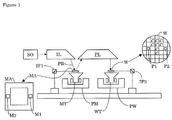
- Figure 1 depicts a lithographic apparatus according to an embodiment of the invention
- Figure 2 shows a schematic embodiment of the lithographic apparatus comprising a controlling arrangement according to an embodiment of the invention
- Figure 3 schematically illustrates the steps for manufacturing a device according to the method of an embodiment of the invention
- Figure 4 schematically illustrates the steps for manufacturing a device according to the method of another embodiment of the invention.
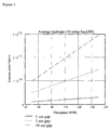
- Figure 5 shows a calculated leakrate load for an article support for clamping a 300 mm wafer.
- Figure 1 schematically depicts a lithographic apparatus according to an embodiment of the invention.
- the apparatus comprises: an illumination system (illuminator) IL for providing a projection beam PB of radiation (e.g. UV or EUV radiation); a first article support or article support structure (e.g. a mask table) MT for supporting patterning device (e.g. a mask) MA and connected to first positioning structure PM for accurately positioning the patterning device with respect to item PL; a second article support (e.g. a wafer table) WT for holding a substrate (e.g. a resist-coated wafer) W and connected to second positioning structure PW for accurately positioning the substrate with respect to item PL; and a projection system (e.g. a reflective projection lens) PL for imaging a pattern imparted to the projection beam PB by patterning device MA onto a target portion C (e.g. comprising one or more dies) of the substrate W.
- a projection system e.g. a reflective projection lens
- the apparatus is of a reflective type (e.g. employing a reflective mask or a programmable mirror array of a type as referred to above).
- the apparatus may be of a transmissive type (e.g. employing a transmissive mask).
- the illuminator IL receives a beam of radiation from a radiation source SO.
- the source and the lithographic apparatus may be separate entities, for example when the source is a plasma discharge source. In such cases, the source is not considered to form part of the lithographic apparatus and the radiation beam is generally passed from the source SO to the illuminator IL with the aid of a radiation collector comprising for example suitable collecting mirrors and/or a spectral purity filter. In other cases the source may be an integral part of the apparatus, for example when the source is a mercury lamp.
- the source SO and the illuminator IL may be referred to as a radiation system.
- the illuminator IL may comprise an adjustor that adjusts the angular intensity distribution of the beam. Generally, at least the outer and/or inner radial extent (commonly referred to as ⁇ -outer and ⁇ -inner, respectively) of the intensity distribution in a pupil plane of the illuminator can be adjusted.
- the illuminator provides a conditioned beam of radiation, referred to as the projection beam PB, having a desired uniformity and intensity distribution in its cross-section.
- the projection beam PB is incident on a patterning device, illustrated in the form of the mask MA, which is held on the mask table MT. Being reflected by the mask MA, the projection beam PB passes through the lens PL, which focuses the beam onto a target portion C of the substrate W.
- the substrate table WT can be moved accurately, e.g. so as to position different target portions C in the path of the beam PB.
- the first positioning structure PM and position sensor IF1 can be used to accurately position the mask MA with respect to the path of the beam PB, e.g. after mechanical retrieval from a mask library, or during a scan.
- the mask table MT may be connected to a short stroke actuator only, or may be fixed.
- Mask MA and substrate W may be aligned using mask alignment marks M1, M2 and substrate alignment marks P1, P2.
- the depicted apparatus can be used in the following preferred modes.
- step mode the mask table MT and the substrate table WT are kept essentially stationary, while an entire pattern imparted to the projection beam is projected onto a target portion C in one go (i.e. a single static exposure).
- the substrate table WT is then shifted in the X and/or Y direction so that a different target portion C can be exposed.
- step mode the maximum size of the exposure field limits the size of the target portion C imaged in a single static exposure.
- the mask table MT and the substrate table WT are scanned synchronously while a pattern imparted to the projection beam is projected onto a target portion C (i.e. a single dynamic exposure).
- the velocity and direction of the substrate table WT relative to the mask table MT is determined by the de-magnification and image reversal characteristics of the projection system PL.
- the maximum size of the exposure field limits the width (in the non-scanning direction) of the target portion in a single dynamic exposure, whereas the length of the scanning motion determines the height (in the scanning direction) of the target portion.
- the mask table MT is kept essentially stationary holding a programmable patterning device, and the substrate table WT is moved or scanned while a pattern imparted to the projection beam is projected onto a target portion C.
- a pulsed radiation source is employed and the programmable patterning device may be updated after each movement of the substrate table WT or in between successive radiation pulses during a scan.
- This mode of operation can be readily applied to maskless lithography that utilizes programmable patterning device, such as a programmable mirror array of a type as referred to above.
- FIG. 2 illustrates schematically the controlling arrangement 1 according to an embodiment of the invention, where a controller 2 is present for controlling an electrostatic clamp 3 and/or a backfill gas feed 4.
- the controller 2 may be a software part that is embodied in the controlling logic of the lithographic apparatus; it may be a separate controlling function or embodied in a general controlling program for controlling the process functions of the lithographic apparatus. Otherwise, it may be embodied in hardware, such a digital and/or analog circuit that is arranged to provide the controlling functions via circuitry that will not be elaborated upon since the design thereof may be implemented without burden when reading the disclosure of this application.
- the clamp 3 may form part of an article support 5, which is illustrated to have a plurality of protrusions 6 such as is described with reference to European Patent No. EP0947884, published October 6, 1999, which is incorporated herein by reference thereto.
- the protrusions 6 provide an ultra flat plane of support, so that during the photolithographic process, an article 7 is kept level in the most optimal way.
- the clamp 3 provides a clamping force, that is, the article 7 is pressed onto the article support 5, for instance, by electrostatic clamping or other clamping methods known in the art.
- one aspect of the invention equally applies to a general flat article to be placed in a projection beam, such as an optical element such as a (reflective or transmissive) reticle, or to a substrate to be irradiated, such as a wafer.
- a projection beam such as an optical element such as a (reflective or transmissive) reticle
- a substrate to be irradiated such as a wafer.
- article handler pins 8 in the art known as e-pins or ejection pins
- e-pins or ejection pins two of them are illustrated with corresponding actuators 9.
- the pins 8 are moved upward so as to contact the article 7, thereby lifting it from the protrusions 6 of the article support 5.
- an article handler (not shown) may contact the article 7 and transport it away from the article support 5.
- the sticking forces between the article 7 and the article support 5 can be compensated to a desired extent or even be neutralized.
- the clamp when the clamp is switched off so that the article 7 is no longer clamped onto the article support 5, due to a force provided by the backfill gas pressure, the binding forces between the article 7 and article support 5 are reduced or cancelled.
- a backfill gas 40 is supplied to a cavity 10 between the article 7 and the article support 5 to enhance thermal contact of the article 7 and the article support 5. Such is beneficial to illumination performance, since overheating of the article 7 is prevented which could result in thermal deformation or even loss.
- the backfill gas 40 is pumped away by a backfill gas pump 11.
- This pump 11 may comprise a separate unit (not shown) for feeding the gas into the cavity 10 and a separate unit (not shown) for extracting the gas from the cavity 10.
- the controller 2 controls the clamp 3 and/or the backfill gas pump 11 pressure so as to release the clamp 3 prior to reducing the backfill gas feed pressure.
- the full pressure of the backfill gas 40 is used to counter the sticking force.
- a typical pressure of 10 mbar such counter force would, for a 300 mm wafer, result in a counter force of 70 N, which is typically enough to release the wafer from the article support 5.
- a conventional reticle such a force would be in the order of 22 N.
- the controller 2 may comprise a presence detector (not shown) for detecting a presence of the article 7 on the article support 5 through measurement of the capacity formed by the electrostatic clamp 3 and the article 7 that is clamped thereby. A variation of the capacity may then be indicative for the presence of the article 7.
- the presence detector may be formed by a sensor that measures a displacement of the pins 8 and/or a releasing force that is exerted by the pins 8.
- the presence detection may be done by a separate detector, for instance through an optical detection. The presence detection is used in controlling the backfill gas feed pump 11.
- the indicated presence of the article 7 may result in a continued or even increased pressure of the backfill gas generated by the feed pump 11 for releasing the article 7 from the article support 5 by use of the backfill gas feed pressure.
- the backfill gas feed pump 11 is controlled to stop feeding backfill gas 40.
- the backfill gas may be used only to provide a lift, for instance, in an embodiment, wherein the clamping is performed by vacuum clamping.
- the clamp 3 is not present and the clamp is formed by pump 11 in suction mode.
- the controller 2 may control the pump 11 to provide a positive pressure by direction of the gas flow.
- backfill gas 40 is fed towards the backside of the article 7 for releasing the article 7 from the article support 5 by use of the backfill gas feed pressure.
- Figure 3 shows a schematic diagram illustrating the inventive steps of the method according to an embodiment of the invention. That is, in a method, where a device is manufactured using a photolithographic process, following a first sequence I, in a first step 12, an article, such as a wafer or (reflective) reticle is clamped onto an article support 5, for undergoing a photolithographic irradiation step. Then, in a second step 13, a backfill gas is supplied to the backside of the article 7. In case the backfill gas is supplied for thermal conduction reasons, this step is conducted prior to the irradiation step. After the first step 12 has been conducted, the clamping force clamps the article 7 to the article support 5.
- a backfill gas is supplied for thermal conduction reasons
- the controller 2 controls the pins 8 to press the article 7.
- the controller 2 controls the pins 8 to lift the article 7 from the support 5.
- the controller 2 controls the clamp 3 to switch off the clamping force. Then, the pressure of the backfill gas is unbalanced, and therefore, an upward force is exerted on the article 7.
- step 17 the pins 8 are physically moving the article 7 in a continuous pressing contact.
- step 15a the backfill gas pressure may be increased, to further assist the pressure exerted by the pins 8.
- step 19 the backfill gas pressure is increased to lift the article 7 from the support 5.
- step 20 the controller 2 controls the clamp 3 to switch off the clamping force. Then, the force exerted on the article 7 is unbalanced, so that the article is moved upward.
- step 21 the pins 8 are physically moving the article 7 in a continuous pressing contact.
- Figure 5 shows a graph representing a calculated leakrate load versus the number of wafers processed per hour (WPH) for an article support for clamping a 300 mm wafer.
- the estimated leakrate is shown for a variety of backfill gas gaps ranging from 1 mu to 10 mu. It is shown that the leakrate is well below 0.15 mbar*l/s that defines the maximum tolerable leakrate for inert gasses in an electrostatically clamped vacuum system.
- vacuum pressure is relative to particular gasses that are present in the environment. For instance, for carbonhydrogens and water, the allowable background pressure is very low, in the order of 1e-9 - 1e-12 millibar.
- an allowable background pressure ranges from 1e-4 mbar - 1e-2 mbar, in particular, a pressure of 1e-3 mbar.
- the relative background pressure may vary in terms of the environment of the apparatus. For instance, where the article support functions in the environment of a wafer support, the vacuum requirements for certain components may be less strict than in the environment where the article support functions as a reticle support. That is, the partial pressures for contaminants (such as CxHy and H20) may differ a factor 100 between optics compartment (including reticle support) and wafer compartment and are much lower than the total pressure (typical numbers are 1e-9 to 1e-12 mbar).
- the upward force provided by the present backfill gas may be beneficially used to lift the article from the article support.
Applications Claiming Priority (2)
| Application Number | Priority Date | Filing Date | Title |
|---|---|---|---|
| US734641 | 2003-12-15 | ||
| US10/734,641 US6897945B1 (en) | 2003-12-15 | 2003-12-15 | Lithographic apparatus and device manufacturing method |
Publications (1)
| Publication Number | Publication Date |
|---|---|
| EP1548502A1 true EP1548502A1 (de) | 2005-06-29 |
Family
ID=34552774
Family Applications (1)
| Application Number | Title | Priority Date | Filing Date |
|---|---|---|---|
| EP04078274A Withdrawn EP1548502A1 (de) | 2003-12-15 | 2004-12-02 | Lithographischer Apparat und Verfahren zur Herstellung einer Vorrichtung |
Country Status (7)
| Country | Link |
|---|---|
| US (2) | US6897945B1 (de) |
| EP (1) | EP1548502A1 (de) |
| JP (2) | JP4477480B2 (de) |
| KR (1) | KR100644419B1 (de) |
| CN (2) | CN1629733A (de) |
| SG (1) | SG112968A1 (de) |
| TW (1) | TWI248562B (de) |
Cited By (2)
| Publication number | Priority date | Publication date | Assignee | Title |
|---|---|---|---|---|
| WO2008093053A1 (en) * | 2007-01-31 | 2008-08-07 | Applied Materials, Inc. | Securing a substrate to an electrostatic chuck |
| EP2006899A2 (de) * | 2006-04-05 | 2008-12-24 | Nikon Corporation | Bühnenvorrichtung, belichtungsvorrichtung, bühnensteuerverfahren, belichtungsverfahren und bauelementeherstellungsverfahren |
Families Citing this family (32)
| Publication number | Priority date | Publication date | Assignee | Title |
|---|---|---|---|---|
| JP2004351527A (ja) * | 2003-05-27 | 2004-12-16 | Koganei Corp | 吸着検出方法および吸着検出装置 |
| EP2267535A1 (de) * | 2003-11-05 | 2010-12-29 | ASML Netherlands BV | Lithographischer Apparat und Verfahren zur Herstellung einer Vorrichtung |
| US6897945B1 (en) * | 2003-12-15 | 2005-05-24 | Asml Netherlands B.V. | Lithographic apparatus and device manufacturing method |
| US20050223973A1 (en) * | 2004-03-30 | 2005-10-13 | Infineon Technologies Ag | EUV lithography system and chuck for releasing reticle in a vacuum isolated environment |
| KR101330922B1 (ko) * | 2004-06-21 | 2013-11-18 | 가부시키가이샤 니콘 | 노광 장치 및 디바이스 제조 방법 |
| US7196775B2 (en) * | 2004-08-23 | 2007-03-27 | Asml Holding N.V. | Patterned mask holding device and method using two holding systems |
| US7041989B1 (en) | 2004-10-22 | 2006-05-09 | Asml Netherlands B.V. | Lithographic apparatus and device manufacturing method |
| US7649611B2 (en) | 2005-12-30 | 2010-01-19 | Asml Netherlands B.V. | Lithographic apparatus and device manufacturing method |
| US20070268476A1 (en) * | 2006-05-19 | 2007-11-22 | Nikon Corporation | Kinematic chucks for reticles and other planar bodies |
| US20070292245A1 (en) * | 2006-05-25 | 2007-12-20 | Nikon Corporation | Stage assembly with secure device holder |
| US7508494B2 (en) * | 2006-12-22 | 2009-03-24 | Asml Netherlands B.V. | Lithographic apparatus and a subtrate table for exciting a shockwave in a substrate |
| FR2912375B1 (fr) * | 2007-02-14 | 2009-12-18 | Eurocopter France | Verin electrique de commande de vol pour aeronef |
| TWI450047B (zh) * | 2007-07-13 | 2014-08-21 | Mapper Lithography Ip Bv | 微影系統、夾緊方法及晶圓台 |
| US8705010B2 (en) | 2007-07-13 | 2014-04-22 | Mapper Lithography Ip B.V. | Lithography system, method of clamping and wafer table |
| TWI337154B (en) * | 2008-04-17 | 2011-02-11 | Gudeng Prec Industral Co Ltd | Gas filling apparatus and gas filling port thereof |
| TWI475594B (zh) | 2008-05-19 | 2015-03-01 | Entegris Inc | 靜電夾頭 |
| JP4786693B2 (ja) * | 2008-09-30 | 2011-10-05 | 三菱重工業株式会社 | ウェハ接合装置およびウェハ接合方法 |
| JP5470601B2 (ja) * | 2009-03-02 | 2014-04-16 | 新光電気工業株式会社 | 静電チャック |
| US8861170B2 (en) | 2009-05-15 | 2014-10-14 | Entegris, Inc. | Electrostatic chuck with photo-patternable soft protrusion contact surface |
| WO2010132640A2 (en) | 2009-05-15 | 2010-11-18 | Entegris, Inc. | Electrostatic chuck with polymer protrusions |
| CN105196094B (zh) | 2010-05-28 | 2018-01-26 | 恩特格林斯公司 | 高表面电阻率静电吸盘 |
| WO2012076207A1 (en) * | 2010-12-08 | 2012-06-14 | Asml Holding N.V. | Electrostatic clamp, lithographic apparatus and method of manufacturing an electrostatic clamp |
| NL2009689A (en) * | 2011-12-01 | 2013-06-05 | Asml Netherlands Bv | Support, lithographic apparatus and device manufacturing method. |
| NL2009858A (en) | 2011-12-27 | 2013-07-01 | Asml Netherlands Bv | Substrate holder, lithographic apparatus, and device manufacturing method. |
| CN103576464B (zh) * | 2012-07-20 | 2016-03-09 | 上海微电子装备有限公司 | 一种推顶机构及具有该推顶机构的光刻装置 |
| JP2014086701A (ja) * | 2012-10-26 | 2014-05-12 | Canon Inc | 保持装置、リソグラフィ装置及び物品の製造方法 |
| NL2011592A (en) | 2012-10-31 | 2014-05-06 | Asml Netherlands Bv | Compensation for patterning device deformation. |
| WO2017139163A1 (en) * | 2016-02-10 | 2017-08-17 | Entegris, Inc. | Wafer contact surface protrusion profile with improved particle performance |
| CN107272351A (zh) * | 2017-07-28 | 2017-10-20 | 武汉华星光电技术有限公司 | 承载装置及具有该承载装置的曝光设备 |
| JP7104531B2 (ja) * | 2018-03-19 | 2022-07-21 | キヤノン株式会社 | 基板保持装置および基板処理装置 |
| EP3575873A1 (de) | 2018-05-28 | 2019-12-04 | ASML Netherlands B.V. | Teilchenstrahlvorrichtung |
| US20220075279A1 (en) * | 2019-02-08 | 2022-03-10 | Asml Netherlands B.V. | Component for Use in a Lithographic Apparatus, Method of Protecting a Component and Method of Protecting Tables in a Lithographic Apparatus |
Citations (5)
| Publication number | Priority date | Publication date | Assignee | Title |
|---|---|---|---|---|
| JPS60235423A (ja) * | 1984-05-08 | 1985-11-22 | Mitsubishi Electric Corp | 半導体製造装置 |
| EP0452222A1 (de) * | 1990-04-12 | 1991-10-16 | Commissariat A L'energie Atomique | Elektrostatischer Substrathalter |
| EP0803904A2 (de) * | 1996-04-25 | 1997-10-29 | Applied Materials, Inc. | Substratträger |
| US6184972B1 (en) * | 1998-09-18 | 2001-02-06 | Nikon Corporation | Substrate transport apparatus, substrate holding apparatus and substrate processing apparatus |
| US6215642B1 (en) * | 1999-03-11 | 2001-04-10 | Nikon Corporation Of Japan | Vacuum compatible, deformable electrostatic chuck with high thermal conductivity |
Family Cites Families (27)
| Publication number | Priority date | Publication date | Assignee | Title |
|---|---|---|---|---|
| US4384918A (en) | 1980-09-30 | 1983-05-24 | Fujitsu Limited | Method and apparatus for dry etching and electrostatic chucking device used therein |
| GB2106325A (en) | 1981-09-14 | 1983-04-07 | Philips Electronic Associated | Electrostatic chuck |
| US4551192A (en) | 1983-06-30 | 1985-11-05 | International Business Machines Corporation | Electrostatic or vacuum pinchuck formed with microcircuit lithography |
| DE3471827D1 (en) | 1983-09-30 | 1988-07-07 | Philips Electronic Associated | Electrostatic chuck and loading method |
| GB2147459A (en) * | 1983-09-30 | 1985-05-09 | Philips Electronic Associated | Electrostatic chuck for semiconductor wafers |
| JPS6272139A (ja) * | 1985-09-26 | 1987-04-02 | Hitachi Electronics Eng Co Ltd | ウエハ吸着装置 |
| JP3238925B2 (ja) | 1990-11-17 | 2001-12-17 | 株式会社東芝 | 静電チャック |
| US5350479A (en) | 1992-12-02 | 1994-09-27 | Applied Materials, Inc. | Electrostatic chuck for high power plasma processing |
| EP0635870A1 (de) | 1993-07-20 | 1995-01-25 | Applied Materials, Inc. | Eine elektrostatische Halteplatte mit einer gerillten Fläche |
| JPH08507196A (ja) | 1994-01-31 | 1996-07-30 | アプライド マテリアルズ インコーポレイテッド | 共形な絶縁体フィルムを有する静電チャック |
| JP3671379B2 (ja) * | 1994-02-03 | 2005-07-13 | アネルバ株式会社 | 静電吸着された被処理基板の離脱機構を持つプラズマ処理装置および静電吸着された被処理基板の離脱方法 |
| TW288253B (de) * | 1994-02-03 | 1996-10-11 | Aneruba Kk | |
| JPH0878512A (ja) * | 1994-09-09 | 1996-03-22 | Hitachi Ltd | 静電吸着装置及び方法 |
| JPH09172055A (ja) * | 1995-12-19 | 1997-06-30 | Fujitsu Ltd | 静電チャック及びウエハの吸着方法 |
| US5923408A (en) | 1996-01-31 | 1999-07-13 | Canon Kabushiki Kaisha | Substrate holding system and exposure apparatus using the same |
| JP3639686B2 (ja) * | 1996-01-31 | 2005-04-20 | キヤノン株式会社 | 基板の保持装置とこれを用いた露光装置、及びデバイスの製造方法 |
| JP2000156400A (ja) * | 1998-11-19 | 2000-06-06 | Matsushita Electric Ind Co Ltd | 基板の分離方法および分離装置 |
| JP4064557B2 (ja) * | 1999-01-07 | 2008-03-19 | 松下電器産業株式会社 | 真空処理装置の基板取り外し制御方法 |
| JP2001196290A (ja) * | 2000-01-13 | 2001-07-19 | Nikon Corp | 静電チャック、ステージ、基板処理装置、荷電粒子線露光装置及びデバイス製造方法 |
| JP2001267400A (ja) * | 2000-03-16 | 2001-09-28 | Kyocera Corp | ウエハ支持部材 |
| JP2002009139A (ja) * | 2000-06-20 | 2002-01-11 | Nikon Corp | 静電チャック |
| JP2002082445A (ja) * | 2000-07-07 | 2002-03-22 | Nikon Corp | ステージ装置及び露光装置 |
| JP4312394B2 (ja) | 2001-01-29 | 2009-08-12 | 日本碍子株式会社 | 静電チャックおよび基板処理装置 |
| US6628503B2 (en) * | 2001-03-13 | 2003-09-30 | Nikon Corporation | Gas cooled electrostatic pin chuck for vacuum applications |
| JP2002313902A (ja) * | 2001-04-18 | 2002-10-25 | Canon Inc | 静電チャック、該静電チャックから基板を離脱する方法 |
| US7105836B2 (en) * | 2002-10-18 | 2006-09-12 | Asml Holding N.V. | Method and apparatus for cooling a reticle during lithographic exposure |
| US6897945B1 (en) * | 2003-12-15 | 2005-05-24 | Asml Netherlands B.V. | Lithographic apparatus and device manufacturing method |
-
2003
- 2003-12-15 US US10/734,641 patent/US6897945B1/en not_active Expired - Lifetime
-
2004
- 2004-11-18 SG SG200407386A patent/SG112968A1/en unknown
- 2004-12-02 EP EP04078274A patent/EP1548502A1/de not_active Withdrawn
- 2004-12-02 TW TW093137213A patent/TWI248562B/zh active
- 2004-12-14 KR KR1020040105355A patent/KR100644419B1/ko active IP Right Grant
- 2004-12-14 CN CNA2004101007964A patent/CN1629733A/zh active Pending
- 2004-12-14 CN CN2012101209250A patent/CN102645852A/zh active Pending
- 2004-12-14 JP JP2004361720A patent/JP4477480B2/ja active Active
-
2005
- 2005-04-06 US US11/099,650 patent/US7187433B2/en not_active Expired - Lifetime
-
2010
- 2010-02-03 JP JP2010022217A patent/JP5118711B2/ja active Active
Patent Citations (5)
| Publication number | Priority date | Publication date | Assignee | Title |
|---|---|---|---|---|
| JPS60235423A (ja) * | 1984-05-08 | 1985-11-22 | Mitsubishi Electric Corp | 半導体製造装置 |
| EP0452222A1 (de) * | 1990-04-12 | 1991-10-16 | Commissariat A L'energie Atomique | Elektrostatischer Substrathalter |
| EP0803904A2 (de) * | 1996-04-25 | 1997-10-29 | Applied Materials, Inc. | Substratträger |
| US6184972B1 (en) * | 1998-09-18 | 2001-02-06 | Nikon Corporation | Substrate transport apparatus, substrate holding apparatus and substrate processing apparatus |
| US6215642B1 (en) * | 1999-03-11 | 2001-04-10 | Nikon Corporation Of Japan | Vacuum compatible, deformable electrostatic chuck with high thermal conductivity |
Non-Patent Citations (1)
| Title |
|---|
| PATENT ABSTRACTS OF JAPAN vol. 010, no. 091 (E - 394) 9 April 1986 (1986-04-09) * |
Cited By (3)
| Publication number | Priority date | Publication date | Assignee | Title |
|---|---|---|---|---|
| EP2006899A2 (de) * | 2006-04-05 | 2008-12-24 | Nikon Corporation | Bühnenvorrichtung, belichtungsvorrichtung, bühnensteuerverfahren, belichtungsverfahren und bauelementeherstellungsverfahren |
| EP2006899A4 (de) * | 2006-04-05 | 2011-12-28 | Nikon Corp | Bühnenvorrichtung, belichtungsvorrichtung, bühnensteuerverfahren, belichtungsverfahren und bauelementeherstellungsverfahren |
| WO2008093053A1 (en) * | 2007-01-31 | 2008-08-07 | Applied Materials, Inc. | Securing a substrate to an electrostatic chuck |
Also Published As
| Publication number | Publication date |
|---|---|
| JP4477480B2 (ja) | 2010-06-09 |
| JP2010109390A (ja) | 2010-05-13 |
| KR20050060006A (ko) | 2005-06-21 |
| TW200523686A (en) | 2005-07-16 |
| US7187433B2 (en) | 2007-03-06 |
| TWI248562B (en) | 2006-02-01 |
| US20050128463A1 (en) | 2005-06-16 |
| CN1629733A (zh) | 2005-06-22 |
| JP5118711B2 (ja) | 2013-01-16 |
| US6897945B1 (en) | 2005-05-24 |
| KR100644419B1 (ko) | 2006-11-10 |
| CN102645852A (zh) | 2012-08-22 |
| JP2005183959A (ja) | 2005-07-07 |
| US20050174555A1 (en) | 2005-08-11 |
| SG112968A1 (en) | 2005-07-28 |
Similar Documents
| Publication | Publication Date | Title |
|---|---|---|
| US7187433B2 (en) | Electrostatic clamp assembly for a lithographic apparatus | |
| EP1530089B1 (de) | Lithographischer Apparat und Vorrichtungs-Halteverfahren | |
| JP5443574B2 (ja) | リソグラフィ装置およびデバイス製造方法 | |
| EP1530088B1 (de) | Lithographischer Apparat | |
| CN108139675B (zh) | 衬底保持器、光刻设备和制造器件的方法 | |
| EP1510868A1 (de) | Lithographischer Apparat und Verfahren zur Herstellung eines Artikels | |
| US7342237B2 (en) | Lithographic apparatus and device manufacturing method | |
| US7019816B2 (en) | Lithographic apparatus, device manufacturing method, and device manufactured thereby | |
| US7019820B2 (en) | Lithographic apparatus and device manufacturing method | |
| JP4531788B2 (ja) | リソグラフィ装置および方法 | |
| US20070178704A1 (en) | Lithographic apparatus and device manufacturing method |
Legal Events
| Date | Code | Title | Description |
|---|---|---|---|
| PUAI | Public reference made under article 153(3) epc to a published international application that has entered the european phase |
Free format text: ORIGINAL CODE: 0009012 |
|
| AK | Designated contracting states |
Kind code of ref document: A1 Designated state(s): AT BE BG CH CY CZ DE DK EE ES FI FR GB GR HU IE IS IT LI LT LU MC NL PL PT RO SE SI SK TR |
|
| AX | Request for extension of the european patent |
Extension state: AL BA HR LV MK YU |
|
| 17P | Request for examination filed |
Effective date: 20050630 |
|
| AKX | Designation fees paid |
Designated state(s): DE FR GB IT NL |
|
| STAA | Information on the status of an ep patent application or granted ep patent |
Free format text: STATUS: THE APPLICATION IS DEEMED TO BE WITHDRAWN |
|
| 18D | Application deemed to be withdrawn |
Effective date: 20090701 |