EP1510868A1 - Lithographischer Apparat und Verfahren zur Herstellung eines Artikels - Google Patents
Lithographischer Apparat und Verfahren zur Herstellung eines Artikels Download PDFInfo
- Publication number
- EP1510868A1 EP1510868A1 EP03077703A EP03077703A EP1510868A1 EP 1510868 A1 EP1510868 A1 EP 1510868A1 EP 03077703 A EP03077703 A EP 03077703A EP 03077703 A EP03077703 A EP 03077703A EP 1510868 A1 EP1510868 A1 EP 1510868A1
- Authority
- EP
- European Patent Office
- Prior art keywords
- protrusions
- supporting
- lithographic apparatus
- boundary
- article
- Prior art date
- Legal status (The legal status is an assumption and is not a legal conclusion. Google has not performed a legal analysis and makes no representation as to the accuracy of the status listed.)
- Withdrawn
Links
Images


Classifications
-
- G—PHYSICS
- G03—PHOTOGRAPHY; CINEMATOGRAPHY; ANALOGOUS TECHNIQUES USING WAVES OTHER THAN OPTICAL WAVES; ELECTROGRAPHY; HOLOGRAPHY
- G03F—PHOTOMECHANICAL PRODUCTION OF TEXTURED OR PATTERNED SURFACES, e.g. FOR PRINTING, FOR PROCESSING OF SEMICONDUCTOR DEVICES; MATERIALS THEREFOR; ORIGINALS THEREFOR; APPARATUS SPECIALLY ADAPTED THEREFOR
- G03F7/00—Photomechanical, e.g. photolithographic, production of textured or patterned surfaces, e.g. printing surfaces; Materials therefor, e.g. comprising photoresists; Apparatus specially adapted therefor
- G03F7/70—Microphotolithographic exposure; Apparatus therefor
- G03F7/70691—Handling of masks or workpieces
- G03F7/707—Chucks, e.g. chucking or un-chucking operations or structural details
-
- G—PHYSICS
- G03—PHOTOGRAPHY; CINEMATOGRAPHY; ANALOGOUS TECHNIQUES USING WAVES OTHER THAN OPTICAL WAVES; ELECTROGRAPHY; HOLOGRAPHY
- G03F—PHOTOMECHANICAL PRODUCTION OF TEXTURED OR PATTERNED SURFACES, e.g. FOR PRINTING, FOR PROCESSING OF SEMICONDUCTOR DEVICES; MATERIALS THEREFOR; ORIGINALS THEREFOR; APPARATUS SPECIALLY ADAPTED THEREFOR
- G03F7/00—Photomechanical, e.g. photolithographic, production of textured or patterned surfaces, e.g. printing surfaces; Materials therefor, e.g. comprising photoresists; Apparatus specially adapted therefor
- G03F7/70—Microphotolithographic exposure; Apparatus therefor
- G03F7/708—Construction of apparatus, e.g. environment aspects, hygiene aspects or materials
- G03F7/70808—Construction details, e.g. housing, load-lock, seals or windows for passing light in or out of apparatus
- G03F7/70825—Mounting of individual elements, e.g. mounts, holders or supports
Definitions
- the present invention relates to a lithographic apparatus and a device manufacturing method. More specifically, the invention relates to a lithographic apparatus comprising: an illumination system for providing a projection beam of radiation; an article support for supporting a flat article to be placed in a beam path of said projection beam of radiation on said article support, comprising a plurality of supporting protrusions defining a protrusion configuration for providing a plane of support; and releasing means for releasing said article from said article support.
- a lithographic apparatus is a machine that applies a desired pattern onto a target portion of a substrate.
- Lithographic apparatus can be used, for example, in the manufacture of integrated circuits (ICs).
- a patterning means such as a mask, may be used to generate a circuit pattern corresponding to an individual layer of the IC, and this pattern can be imaged onto a target portion (e.g. comprising part of, one or several dies) on a substrate (e.g. a silicon wafer) that has a layer of radiation-sensitive material (resist).
- a single substrate will contain a network of adjacent target portions that are successively exposed.
- lithographic apparatus include so-called steppers, in which each target portion is irradiated by exposing an entire pattern onto the target portion in one go, and so-called scanners, in which each target portion is irradiated by scanning the pattern through the projection beam in a given direction (the "scanning"-direction) while synchronously scanning the substrate parallel or anti-parallel to this direction.
- an article such as a wafer or reticle is clamped on an article support by a clamping force, that may range from vacuum pressure forces, electrostatic forces, intermolecular binding forces or just gravity force.
- the article support defines a plane, in the form of a plurality of protrusions defining an even flat surface on which the wafer or reticle is held. Tiny variations in the height of these protrusions are detrimental to image resolution, since a small deflection of the article from an ideal plane orientation may result in rotation of the wafer and a resulting overlay error due to this rotation.
- height variations of the article support may result in height variation of the article that is supported thereby. During the lithographic process, such height variations may affect image resolution due to a limited focal distance of the projection system. Therefore it is very critical to have an ideal flat article support.
- European patent application EP0947884 describes a lithographic apparatus having a substrate holder wherein protrusions are arranged to improve the flatness of the substrate. These protrusions have a general diameter of 0.5 mm and are located generally at a distance of 3 mm away from each other and thereby form a bed of supporting members that support the substrate. Due to the relative large spaces in between the protrusions, contaminations possibly present generally do not form an obstruction for the flatness of the substrate, since these will be lying in between the protrusions and will not lift the substrate locally.
- the said "article” may be any of the above mentioned terms wafer, reticle, mask, or substrate, more specifically terms such as
- a common way to release said article from said article support is by stepping up a release force exerted by exerted by an ejection pin mechanism (e-pins), which engages at the article and provide a releasing force to disengage the article from the article support.
- e-pins ejection pin mechanism
- the energy that is built up in the article during this stepping up is converted into displacement by subsequent release of the article surface from the article support surface.
- this built up energy may also cause damage to the article or article support.
- the invention aims to overcome this problem by providing a photolithographic machine, wherein the release energy, when the article is finally released from the wafer holder, is not detrimental for the article support, in particular for the supporting protrusions defining said plane of support.
- a lithographic apparatus according to the preamble of claim 1, wherein said article support comprises at least one protective member located near a boundary of said plurality of protrusions so as to protect at least a boundary portion of said plurality of protrusions during release.
- said energy is absorbed by a zone of the wafer holder where flatness is not crucial.
- flatness can be maintained for the protrusions defining the plane of support.
- said protective member is formed by a boundary portion of supporting protrusions having a supporting area that is larger than a supporting area of a supporting protrusion away from said boundary. Since the supporting area is larger, a small wear of this area near the boundary thereof has relative little effect and will not affect the supporting area as much as a protrusions having a "standard" supporting area.
- the supporting area of said plurality of protrusions viewed in a direction away from said boundary, gradually decreases with a distance of said protrusions to said boundary.
- the load distribution is made more continuous towards the protrusions away from the boundary.
- said supporting area may range from 2-50 times a supporting area of a supporting protrusion away from said boundary.
- a plurality of said supporting protrusions each comprise a base cylinder of a first diameter and a supporting top cylinder of a second diameter smaller or equal to said first diameter, wherein the top cylinders of the protrusions forming a protective member are larger in diameter than the top cylinders of protrusions away from the boundary.
- said protective member defines a first gap between said plane of support and said protective member, so that said protective member contacts said article only during release thereof.
- This gap may range in a range of 0.5 -2.5 um, preferably 1 um.
- said protective member extends away from said boundary, more preferably, said protective member has a strip form extending away from said boundary.
- a plurality of said supporting protrusions each comprise a base cylinder of a first diameter and a supporting top cylinder of a second diameter that is smaller than said first diameter, wherein the top cylinders has a length equal to said first gap, so that said protective member is formed by said base cylinder of said protrusion.
- said article support may comprise a boundary wall adjacent to said plurality of supporting protrusions, said boundary wall providing a second gap between said plane of support and said wall for providing a leaking seal, said second gap being larger than said first gap.
- Said protective member may traverse said boundary wall. Specifically, since the protective member may traverse said wall only on selected places, for instance, every third to tenth protrusion along said boundary, such a traversal does not affect the leaking seal properties in an adverse manner.
- lithographic apparatus in the manufacture of ICs, it should be understood that the lithographic apparatus described herein may have other applications, such as the manufacture of integrated optical systems, guidance and detection patterns for magnetic domain memories, liquid-crystal displays (LCDs), thin-film magnetic heads, etc.
- LCDs liquid-crystal displays
- any use of the terms “wafer” or “die” herein may be considered as synonymous with the more general terms “substrate” or "target portion”, respectively.
- the substrate referred to herein may be processed, before or after exposure, in for example a track (a tool that typically applies a layer of resist to a substrate and develops the exposed resist) or a metrology or inspection tool.
- the disclosure herein may be applied to such and other substrate processing tools.
- the substrate may be processed more than once, for example in order to create a multi-layer IC, so that the term substrate used herein may also refer to a substrate that already contains multiple processed layers.
- UV radiation e.g. having a wavelength of 365, 248, 193, 157 or 126 nm
- EUV extreme ultra-violet
- particle beams such as ion beams or electron beams.
- patterning means used herein should be broadly interpreted as referring to means that can be used to impart a projection beam with a pattern in its cross-section such as to create a pattern in a target portion of the substrate. It should be noted that the pattern imparted to the projection beam may not exactly correspond to the desired pattern in the target portion of the substrate. Generally, the pattern imparted to the projection beam will correspond to a particular functional layer in a device being created in the target portion, such as an integrated circuit.
- Patterning means may be transmissive or reflective.
- Examples of patterning means include masks, programmable mirror arrays, and programmable LCD panels.
- Masks are well known in lithography, and include mask types such as binary, alternating phase-shift, and attenuated phase-shift, as well as various hybrid mask types.
- An example of a programmable mirror array employs a matrix arrangement of small mirrors, each of which can be individually tilted so as to reflect an incoming radiation beam in different directions; in this manner, the reflected beam is patterned.
- the support structure may be a frame or table, for example, which may be fixed or movable as required and which may ensure that the patterning means is at a desired position, for example with respect to the projection system. Any use of the terms "reticle” or “mask” herein may be considered synonymous with the more general term "patterning means”.
- projection system used herein should be broadly interpreted as encompassing various types of projection system, including refractive optical systems, reflective optical systems, and catadioptric optical systems, as appropriate for example for the exposure radiation being used, or for other factors such as the use of an immersion fluid or the use of a vacuum. Any use of the term “lens” herein may be considered as synonymous with the more general term “projection system”.
- the illumination system may also encompass various types of optical components, including refractive, reflective, and catadioptric optical components for directing, shaping, or controlling the projection beam of radiation, and such components may also be referred to below, collectively or singularly, as a "lens”.
- the lithographic apparatus may be of a type having two (dual stage) or more substrate tables (and/or two or more mask tables). In such "multiple stage” machines the additional tables may be used in parallel, or preparatory steps may be carried out on one or more tables while one or more other tables are being used for exposure.
- the lithographic apparatus may also be of a type wherein the substrate is immersed in a liquid having a relatively high refractive index, e.g. water, so as to fill a space between the final element of the projection system and the substrate.
- Immersion liquids may also be applied to other spaces in the lithographic apparatus, for example, between the mask and the first element of the projection system. Immersion techniques are well known in the art for increasing the numerical aperture of projection systems.
- Figure 1 schematically depicts a lithographic apparatus according to a particular embodiment of the invention.
- the apparatus comprises:
- the apparatus is of a reflective type (e.g. employing a reflective mask or a programmable mirror array of a type as referred to above).
- the apparatus may be of a transmissive type (e.g. employing a transmissive mask).
- the illuminator IL receives a beam of radiation from a radiation source SO.
- the source and the lithographic apparatus may be separate entities, for example when the source is a plasma discharge source. In such cases, the source is not considered to form part of the lithographic apparatus and the radiation beam is generally passed from the source SO to the illuminator IL with the aid of a radiation collector comprising for example suitable collecting mirrors and/or a spectral purity filter. In other cases the source may be integral part of the apparatus, for example when the source is a mercury lamp.
- the source SO and the illuminator IL may be referred to as a radiation system.
- the illuminator IL may comprise adjusting means for adjusting the angular intensity distribution of the beam.
- adjusting means for adjusting the angular intensity distribution of the beam Generally, at least the outer and/or inner radial extent (commonly referred to as ⁇ -outer and ⁇ -inner, respectively) of the intensity distribution in a pupil plane of the illuminator can be adjusted.
- the illuminator provides a conditioned beam of radiation, referred to as the projection beam PB, having a desired uniformity and intensity distribution in its cross-section.
- the projection beam PB is incident on the mask MA, which is held on the mask table MT. Being reflected by the mask MA, the projection beam PB passes through the lens PL, which focuses the beam onto a target portion C of the substrate W.
- the substrate table WT can be moved accurately, e.g. so as to position different target portions C in the path of the beam PB.
- the first positioning means PM and position sensor IF1 can be used to accurately position the mask MA with respect to the path of the beam PB, e.g. after mechanical retrieval from a mask library, or during a scan.
- the mask table MT may be connected to a short stroke actuator only, or may be fixed.
- Mask MA and substrate W may be aligned using mask alignment marks M1, M2 and substrate alignment marks P1, P2.
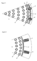
- FIG 2 a schematic plan view is illustrated of a segment of an article support 1 according to the invention.
- a plurality of protrusions 2 is pictured, the protrusions 2 are oriented in substantially concentric circles. To improve the intelligibility, only a few protrusions 2 are referenced in the figures.
- a surrounding wall 3 is dimensioned to provide a leaking seal as is explained more in extenso in the referenced EP0947884. That is, the wall 3 encloses the protrusion configuration and is generally circular in form, and has a uniform height that provides a gap ranging from 1 -5 um, preferably 3 um between the plane of support and said wall 3 for providing a leaking seal.
- Such a leaking seal is preferential in a configuration where an article such as a wafer to be illuminated is clamped by vacuum pressure on the article support.
- an article such as a wafer to be illuminated is clamped by vacuum pressure on the article support.
- the vacuum near the boundaries tends to provide a better load to the article, providing better imaging properties due to an improved flatness of the article, being a wafer or a reticle.
- the protrusions 2 are formed by a base cylinder 4 of a first diameter and a supporting top cylinder 5 of a second diameter smaller or equal to said first diameter.
- the base cylinder 4 has a diameter of 0.5 mm and the top cylinder 5 has a diameter of 0.15 mm and a length of 3 um, substantially equal to the gap provided by the leaking seal.
- the protrusions 2 define a protrusion configuration for providing a plane of support of an article (not shown) to be supported on the article support. Such plane of support is flat, that is, defines a height variation of less than 100 nm, preferably less than 10 nm.
- the top cylinders 5' of the protrusions near the boundary wall 3 form a protective member, since they are larger in diameter than the top cylinders 5 of protrusions away from the boundary.
- the protrusions near the boundary wall 3protect are thus more robust in form, so that wear during release does not affect the protrusions as it would with protrusions with a lesser diameter that are positioned more towards the center of the article support.
- an amount of wear per release of the wafer has a strongly reduced effect on the outer protrusions according the design of the inventive embodiment, since their supporting area is larger than a supporting area of a supporting protrusion away from said boundary wall 3 ranging from 2-50 times, preferably 10 times a supporting area of a supporting protrusion away from said boundary wall 3.
- a gradual change in diameter is shown of the protrusions 5" and 5''' more distant from the boundary wall 3, since, viewed in a direction away from boundary wall 3, the supporting area formed by the top cylinders 5', 5", 5''' of the protrusions 2 gradually decrease with the distance from the boundary wall 3.
- such a decrease in diameter with distance may be formed by eight rows of consecutive protrusions 2, wherein, for example the first row from the boundary wall 3 has a top cylinder diameter that is equal to the base cylinder diameter, and then, consecutively, the diameter of the top cylinders of subsequent more inner rows decreases from 0.5 to 0.15 mm in steps whereby the surface area per burl decreases linear per row.
- the embodiment of Figure 2 is relatively easily manufacturable, since it offers protection from wear whereas the design comprises only two different altitudes, that is, the altitude of the boundary wall 3 and base cylinders 4 at a first altitude and the altitude of the top cylinder 5 at a second altitude, differing preferably about 3 um from said first altitude.
- Figure 3 shows an embodiment wherein a further altitude is introduced, well in between said first and second altitude as discussed with reference to Figure 2.
- the diameters of the base cylinders 4 and top cylinders 5 are kept relatively constant throughout the whole design, but the height of the top cylinders is varied for the protrusions 2' in the direct vicinity of the boundary, in the embodiment of Figure 3 also formed by the boundary wall 3.
- the base cylinder 4' of the boundary protrusions 2' is lengthened and the top cylinder 5' of the boundary is shortened.
- the resultant protrusion 2' comprises a support area that lies within the plane of support, but with the base cylinder defining only a small gap of approximately 0.5 - 2.5 um, preferably 1 um between the base cylinder 4 and the plane of support.
- the base cylinder 4' forms a protective member that contacts the article only during release thereof.
- the load distribution is therefore not affected by the presence of the protective element formed by the base cylinder 4', and during release, on the slightest tilt of the article during release, the base cylinder 4' is contacted so that the supporting area of top cylinder 5' of the protrusion 2 is kept intact.
- Such tilt may be expressed in terms of rotation of the article surface, which may amount to maximum values as much as 2-3 mrad.
- Figure 4 shows a configuration wherein only some of the boundary protrusions are provided with a protective contact zone as explained with reference to Figure 3.
- every third protrusion has a protective zone 4', that is extended through the wall 3 towards the edge of the article, that extends generally beyond said boundary wall 3 in radial direction.
- the extended protective zones 4' are formed in a radial strip form that extends well beyond the wall 3, for instance up to a length where the article edge is present in a condition where the article is supported on the article support.
- Figure 5 shows another embodiment according to the invention, wherein the protective member is formed by a contact zone 6 that is separate from the existent protrusion and wall configuration.
- the contact zone 6 is formed by an area located at substantially the same altitude as the protective member 4' in Figure 3 and Figure 4. That is, this contact zone 6 also provides a small gap of preferably 1 um between said contact zone 6 and the plane of support, so that the contact zone 6 contacts the article only during release thereof.
- the contact zone 6 is designed in the area outside the surrounding wall 3. In this area, normally, the edge of the article is present, so that upon release, the edge of the article is supported on the contact area 6 without wearing or damaging the protrusions 2 and thus protecting the protrusions 2.
Landscapes
- Physics & Mathematics (AREA)
- General Physics & Mathematics (AREA)
- Health & Medical Sciences (AREA)
- Engineering & Computer Science (AREA)
- Environmental & Geological Engineering (AREA)
- Epidemiology (AREA)
- Public Health (AREA)
- Exposure And Positioning Against Photoresist Photosensitive Materials (AREA)
- Container, Conveyance, Adherence, Positioning, Of Wafer (AREA)
- Exposure Of Semiconductors, Excluding Electron Or Ion Beam Exposure (AREA)
Priority Applications (3)
| Application Number | Priority Date | Filing Date | Title |
|---|---|---|---|
| EP03077703A EP1510868A1 (de) | 2003-08-29 | 2003-08-29 | Lithographischer Apparat und Verfahren zur Herstellung eines Artikels |
| US10/926,402 US7119885B2 (en) | 2003-08-29 | 2004-08-26 | Lithographic apparatus and device manufacturing method |
| JP2004247641A JP4340204B2 (ja) | 2003-08-29 | 2004-08-27 | リトグラフ装置およびデバイス製造方法 |
Applications Claiming Priority (1)
| Application Number | Priority Date | Filing Date | Title |
|---|---|---|---|
| EP03077703A EP1510868A1 (de) | 2003-08-29 | 2003-08-29 | Lithographischer Apparat und Verfahren zur Herstellung eines Artikels |
Publications (1)
| Publication Number | Publication Date |
|---|---|
| EP1510868A1 true EP1510868A1 (de) | 2005-03-02 |
Family
ID=34089672
Family Applications (1)
| Application Number | Title | Priority Date | Filing Date |
|---|---|---|---|
| EP03077703A Withdrawn EP1510868A1 (de) | 2003-08-29 | 2003-08-29 | Lithographischer Apparat und Verfahren zur Herstellung eines Artikels |
Country Status (3)
| Country | Link |
|---|---|
| US (1) | US7119885B2 (de) |
| EP (1) | EP1510868A1 (de) |
| JP (1) | JP4340204B2 (de) |
Cited By (1)
| Publication number | Priority date | Publication date | Assignee | Title |
|---|---|---|---|---|
| JP2015508229A (ja) * | 2012-02-03 | 2015-03-16 | エーエスエムエル ネザーランズ ビー.ブイ. | 基板ホルダ、リソグラフィ装置、デバイス製造方法及び基板ホルダの製造方法 |
Families Citing this family (15)
| Publication number | Priority date | Publication date | Assignee | Title |
|---|---|---|---|---|
| JP4636807B2 (ja) * | 2004-03-18 | 2011-02-23 | キヤノン株式会社 | 基板保持装置およびそれを用いた露光装置 |
| KR100723483B1 (ko) * | 2005-02-03 | 2007-05-31 | 삼성전자주식회사 | 레티클 로딩장치 및 로딩방법 |
| JP2006261156A (ja) * | 2005-03-15 | 2006-09-28 | Canon Inc | 原版保持装置およびそれを用いた露光装置 |
| EP1840657A1 (de) * | 2006-03-28 | 2007-10-03 | Carl Zeiss SMT AG | Halterungsstruktur zur vorübergehenden Halterung eines Substrats |
| KR20080026499A (ko) * | 2006-09-20 | 2008-03-25 | 캐논 가부시끼가이샤 | 기판보유장치 |
| JP4899879B2 (ja) * | 2007-01-17 | 2012-03-21 | 東京エレクトロン株式会社 | 基板処理装置、基板処理方法及び記憶媒体 |
| US20080262488A1 (en) * | 2007-04-12 | 2008-10-23 | Rhytec Limited | Tissue treatment system and a method of cosmetic tissue treatment |
| JP4782744B2 (ja) * | 2007-08-24 | 2011-09-28 | 京セラ株式会社 | 吸着部材、吸着装置および吸着方法 |
| US8345242B2 (en) * | 2008-10-28 | 2013-01-01 | Molecular Imprints, Inc. | Optical system for use in stage control |
| US9329497B2 (en) * | 2011-02-01 | 2016-05-03 | Asml Netherlands B.V. | Substrate table, lithographic apparatus and device manufacturing method |
| NL2009189A (en) | 2011-08-17 | 2013-02-19 | Asml Netherlands Bv | Support table for a lithographic apparatus, lithographic apparatus and device manufacturing method. |
| JP6867149B2 (ja) * | 2015-12-25 | 2021-04-28 | 日本特殊陶業株式会社 | 基板保持部材 |
| US11270906B2 (en) | 2017-10-27 | 2022-03-08 | Asml Holding N.V. | Burls with altered surface topography for holding an object in lithography applications |
| CN111465901A (zh) * | 2017-12-13 | 2020-07-28 | Asml荷兰有限公司 | 用于光刻设备中的衬底保持器 |
| KR102607809B1 (ko) * | 2021-06-25 | 2023-11-29 | 세메스 주식회사 | 지지 유닛, 이를 포함하는 베이크 장치 및 기판 처리 장치 |
Citations (7)
| Publication number | Priority date | Publication date | Assignee | Title |
|---|---|---|---|---|
| US5374829A (en) * | 1990-05-07 | 1994-12-20 | Canon Kabushiki Kaisha | Vacuum chuck |
| JPH08181054A (ja) | 1994-12-26 | 1996-07-12 | Nikon Corp | ステージ装置及びその制御方法 |
| US5923408A (en) | 1996-01-31 | 1999-07-13 | Canon Kabushiki Kaisha | Substrate holding system and exposure apparatus using the same |
| EP0947884A2 (de) * | 1998-03-31 | 1999-10-06 | Asm Lithography B.V. | Lithographischer Projektionsapparat mit Substrathalter |
| US6183189B1 (en) * | 1998-11-27 | 2001-02-06 | Chartered Semiconductor Manufacturing, Ltd. | Self aligning wafer chuck design for wafer processing tools |
| US20020008864A1 (en) * | 2000-03-13 | 2002-01-24 | Nikon Corporation | Substrate holding apparatus and exposure apparatus including substrate holding apparatus |
| EP1378936A2 (de) * | 2002-07-01 | 2004-01-07 | Fraunhofer-Gesellschaft zur Förderung der angewandten Forschung e.V. | Elektrostatisches Halteelement |
Family Cites Families (7)
| Publication number | Priority date | Publication date | Assignee | Title |
|---|---|---|---|---|
| US4551192A (en) * | 1983-06-30 | 1985-11-05 | International Business Machines Corporation | Electrostatic or vacuum pinchuck formed with microcircuit lithography |
| JPH07153825A (ja) * | 1993-11-29 | 1995-06-16 | Toto Ltd | 静電チャック及びこの静電チャックを用いた被吸着体の処理方法 |
| US5583736A (en) * | 1994-11-17 | 1996-12-10 | The United States Of America As Represented By The Department Of Energy | Micromachined silicon electrostatic chuck |
| US5825607A (en) * | 1996-05-08 | 1998-10-20 | Applied Materials, Inc. | Insulated wafer spacing mask for a substrate support chuck and method of fabricating same |
| US6030282A (en) * | 1998-06-23 | 2000-02-29 | Advanced Micro Devices, Inc. | Method and apparatus for holding, grinding and polishing a packaged semiconductor die |
| EP1077393A2 (de) * | 1999-08-19 | 2001-02-21 | Canon Kabushiki Kaisha | System zum Anziehen und Halten eines Substrats zur Verwendung in einem Belichtungsapparat |
| JP3894562B2 (ja) * | 2003-10-01 | 2007-03-22 | キヤノン株式会社 | 基板吸着装置、露光装置およびデバイス製造方法 |
-
2003
- 2003-08-29 EP EP03077703A patent/EP1510868A1/de not_active Withdrawn
-
2004
- 2004-08-26 US US10/926,402 patent/US7119885B2/en not_active Expired - Lifetime
- 2004-08-27 JP JP2004247641A patent/JP4340204B2/ja not_active Expired - Lifetime
Patent Citations (7)
| Publication number | Priority date | Publication date | Assignee | Title |
|---|---|---|---|---|
| US5374829A (en) * | 1990-05-07 | 1994-12-20 | Canon Kabushiki Kaisha | Vacuum chuck |
| JPH08181054A (ja) | 1994-12-26 | 1996-07-12 | Nikon Corp | ステージ装置及びその制御方法 |
| US5923408A (en) | 1996-01-31 | 1999-07-13 | Canon Kabushiki Kaisha | Substrate holding system and exposure apparatus using the same |
| EP0947884A2 (de) * | 1998-03-31 | 1999-10-06 | Asm Lithography B.V. | Lithographischer Projektionsapparat mit Substrathalter |
| US6183189B1 (en) * | 1998-11-27 | 2001-02-06 | Chartered Semiconductor Manufacturing, Ltd. | Self aligning wafer chuck design for wafer processing tools |
| US20020008864A1 (en) * | 2000-03-13 | 2002-01-24 | Nikon Corporation | Substrate holding apparatus and exposure apparatus including substrate holding apparatus |
| EP1378936A2 (de) * | 2002-07-01 | 2004-01-07 | Fraunhofer-Gesellschaft zur Förderung der angewandten Forschung e.V. | Elektrostatisches Halteelement |
Non-Patent Citations (1)
| Title |
|---|
| PATENT ABSTRACTS OF JAPAN vol. 1996, no. 11 29 November 1996 (1996-11-29) * |
Cited By (12)
| Publication number | Priority date | Publication date | Assignee | Title |
|---|---|---|---|---|
| JP2015508229A (ja) * | 2012-02-03 | 2015-03-16 | エーエスエムエル ネザーランズ ビー.ブイ. | 基板ホルダ、リソグラフィ装置、デバイス製造方法及び基板ホルダの製造方法 |
| US9442395B2 (en) | 2012-02-03 | 2016-09-13 | Asml Netherlands B.V. | Substrate holder, lithographic apparatus, device manufacturing method, and method of manufacturing a substrate holder |
| US9507274B2 (en) | 2012-02-03 | 2016-11-29 | Asml Netherlands B.V. | Substrate holder and method of manufacturing a substrate holder |
| US9737934B2 (en) | 2012-02-03 | 2017-08-22 | Asml Netherlands B.V. | Substrate holder and method of manufacturing a substrate holder |
| US10245641B2 (en) | 2012-02-03 | 2019-04-02 | Asml Netherlands B.V. | Substrate holder, lithographic apparatus, device manufacturing method, and method of manufacturing a substrate holder |
| US10875096B2 (en) | 2012-02-03 | 2020-12-29 | Asml Netherlands B.V. | Substrate holder and method of manufacturing a substrate holder |
| US10898955B2 (en) | 2012-02-03 | 2021-01-26 | Asme Netherlands B.V. | Substrate holder, lithographic apparatus, device manufacturing method, and method of manufacturing a substrate holder |
| US11235388B2 (en) | 2012-02-03 | 2022-02-01 | Asml Netherlands B.V. | Substrate holder, lithographic apparatus, device manufacturing method, and method of manufacturing a substrate holder |
| US11376663B2 (en) | 2012-02-03 | 2022-07-05 | Asml Netherlands B.V. | Substrate holder and method of manufacturing a substrate holder |
| US11628498B2 (en) | 2012-02-03 | 2023-04-18 | Asml Netherlands B.V. | Substrate holder, lithographic apparatus, device manufacturing method, and method of manufacturing a substrate holder |
| US11754929B2 (en) | 2012-02-03 | 2023-09-12 | Asml Netherlands B.V. | Substrate holder and method of manufacturing a substrate holder |
| US11960213B2 (en) | 2012-02-03 | 2024-04-16 | Asml Netherlands B.V. | Substrate holder, lithographic apparatus, device manufacturing method, and method of manufacturing a substrate holder |
Also Published As
| Publication number | Publication date |
|---|---|
| US7119885B2 (en) | 2006-10-10 |
| JP4340204B2 (ja) | 2009-10-07 |
| US20050117141A1 (en) | 2005-06-02 |
| JP2005079586A (ja) | 2005-03-24 |
Similar Documents
| Publication | Publication Date | Title |
|---|---|---|
| KR100656580B1 (ko) | 리소그래피 장치 및 디바이스 제조방법 | |
| US7633600B2 (en) | Lithographic apparatus and device manufacturing method | |
| KR100700372B1 (ko) | 리소그래피 장치 및 디바이스 제조방법 | |
| US7119885B2 (en) | Lithographic apparatus and device manufacturing method | |
| JP4399391B2 (ja) | リソグラフィック装置、物品サポート部材及び方法 | |
| US20060158638A1 (en) | Lithographic apparatus, device manufacturing method, and device manufactured thereby | |
| KR20060052064A (ko) | 리소그래피 장치 및 디바이스 제조방법 | |
| US7030967B2 (en) | Lithographic apparatus, device manufacturing method and substrate holder | |
| JP2011023749A (ja) | リソグラフィ装置およびデバイス製造方法 | |
| EP1498777A1 (de) | Substrathalter und lithographischer Projektionsapparat | |
| US7019816B2 (en) | Lithographic apparatus, device manufacturing method, and device manufactured thereby | |
| EP1491953A1 (de) | Lithographischer Apparat, Verfahren zur Herstellung eines Artikels und damit erzeugter Artikel | |
| US6960775B1 (en) | Lithographic apparatus, device manufacturing method and device manufactured thereby | |
| JP2006237606A (ja) | リソグラフィ装置及び装置製造方法 | |
| EP2037324A2 (de) | Lithographische Vorrichtung und Verfahren | |
| US7019820B2 (en) | Lithographic apparatus and device manufacturing method | |
| KR20030075133A (ko) | 리소그래피장치 및 디바이스 제조방법 | |
| WO2007110777A2 (en) | Lithographic apparatus and patterning device | |
| WO2008147175A1 (en) | Lithographic apparatus and device manufacturing method | |
| EP1528432B1 (de) | Lithographischer Apparat und Verfahren zur Herstellung einer Vorrichtung | |
| EP1431831B1 (de) | Lithographischer Apparat, Verfahren zur Herstellung einer Vorrichtung und Substrathalter | |
| EP1482370B1 (de) | Substrathalter für einen lithographischen Apparat | |
| US20100178612A1 (en) | Lithographic apparatus and device manufacturing method | |
| JP4597925B2 (ja) | リソグラフィー投影装置 | |
| JP2007251133A (ja) | リソグラフィ装置およびデバイス製造方法 |
Legal Events
| Date | Code | Title | Description |
|---|---|---|---|
| PUAI | Public reference made under article 153(3) epc to a published international application that has entered the european phase |
Free format text: ORIGINAL CODE: 0009012 |
|
| AK | Designated contracting states |
Kind code of ref document: A1 Designated state(s): AT BE BG CH CY CZ DE DK EE ES FI FR GB GR HU IE IT LI LU MC NL PT RO SE SI SK TR |
|
| AX | Request for extension of the european patent |
Extension state: AL LT LV MK |
|
| 17P | Request for examination filed |
Effective date: 20050524 |
|
| AKX | Designation fees paid |
Designated state(s): DE FR GB IT NL |
|
| GRAP | Despatch of communication of intention to grant a patent |
Free format text: ORIGINAL CODE: EPIDOSNIGR1 |
|
| RTI1 | Title (correction) |
Free format text: LITHOGRAPHIC APPARATUS |
|
| STAA | Information on the status of an ep patent application or granted ep patent |
Free format text: STATUS: THE APPLICATION IS DEEMED TO BE WITHDRAWN |
|
| 18D | Application deemed to be withdrawn |
Effective date: 20090717 |