EP1533896B1 - Piezoelektrisches Element als solches sowie in Zusammensetzung, in einem Filter, in einem Duplexer oder in Kommunikationsvorrichtung - Google Patents
Piezoelektrisches Element als solches sowie in Zusammensetzung, in einem Filter, in einem Duplexer oder in Kommunikationsvorrichtung Download PDFInfo
- Publication number
- EP1533896B1 EP1533896B1 EP04027275A EP04027275A EP1533896B1 EP 1533896 B1 EP1533896 B1 EP 1533896B1 EP 04027275 A EP04027275 A EP 04027275A EP 04027275 A EP04027275 A EP 04027275A EP 1533896 B1 EP1533896 B1 EP 1533896B1
- Authority
- EP
- European Patent Office
- Prior art keywords
- piezoelectric
- piezoelectric element
- layer
- electrode layer
- piezoelectric vibrating
- Prior art date
- Legal status (The legal status is an assumption and is not a legal conclusion. Google has not performed a legal analysis and makes no representation as to the accuracy of the status listed.)
- Expired - Fee Related
Links
- 239000002131 composite material Substances 0.000 title claims description 45
- 238000004891 communication Methods 0.000 title claims description 15
- 239000000758 substrate Substances 0.000 claims description 82
- 238000010030 laminating Methods 0.000 claims description 33
- 230000002093 peripheral effect Effects 0.000 claims description 13
- 238000012545 processing Methods 0.000 claims description 4
- 230000004044 response Effects 0.000 description 31
- 230000000694 effects Effects 0.000 description 17
- 238000010586 diagram Methods 0.000 description 11
- 230000001902 propagating effect Effects 0.000 description 11
- 230000008878 coupling Effects 0.000 description 10
- 238000010168 coupling process Methods 0.000 description 10
- 238000005859 coupling reaction Methods 0.000 description 10
- VYPSYNLAJGMNEJ-UHFFFAOYSA-N Silicium dioxide Chemical compound O=[Si]=O VYPSYNLAJGMNEJ-UHFFFAOYSA-N 0.000 description 9
- 239000003990 capacitor Substances 0.000 description 8
- 239000000853 adhesive Substances 0.000 description 6
- 230000001070 adhesive effect Effects 0.000 description 6
- 239000000463 material Substances 0.000 description 6
- 230000015556 catabolic process Effects 0.000 description 4
- 229910052681 coesite Inorganic materials 0.000 description 4
- 229910052906 cristobalite Inorganic materials 0.000 description 4
- 238000005530 etching Methods 0.000 description 4
- 230000000149 penetrating effect Effects 0.000 description 4
- 239000000377 silicon dioxide Substances 0.000 description 4
- 229910052682 stishovite Inorganic materials 0.000 description 4
- 229910052905 tridymite Inorganic materials 0.000 description 4
- 230000005540 biological transmission Effects 0.000 description 3
- 230000008859 change Effects 0.000 description 3
- 239000010408 film Substances 0.000 description 3
- 238000000034 method Methods 0.000 description 3
- BASFCYQUMIYNBI-UHFFFAOYSA-N platinum Chemical compound [Pt] BASFCYQUMIYNBI-UHFFFAOYSA-N 0.000 description 3
- PIGFYZPCRLYGLF-UHFFFAOYSA-N Aluminum nitride Chemical compound [Al]#N PIGFYZPCRLYGLF-UHFFFAOYSA-N 0.000 description 2
- XUIMIQQOPSSXEZ-UHFFFAOYSA-N Silicon Chemical compound [Si] XUIMIQQOPSSXEZ-UHFFFAOYSA-N 0.000 description 2
- 230000000052 comparative effect Effects 0.000 description 2
- 230000005684 electric field Effects 0.000 description 2
- 239000010931 gold Substances 0.000 description 2
- 229910052451 lead zirconate titanate Inorganic materials 0.000 description 2
- 238000004519 manufacturing process Methods 0.000 description 2
- 239000004065 semiconductor Substances 0.000 description 2
- 229910052710 silicon Inorganic materials 0.000 description 2
- 239000010703 silicon Substances 0.000 description 2
- 239000000126 substance Substances 0.000 description 2
- 239000010409 thin film Substances 0.000 description 2
- 239000010936 titanium Substances 0.000 description 2
- KRHYYFGTRYWZRS-UHFFFAOYSA-N Fluorane Chemical compound F KRHYYFGTRYWZRS-UHFFFAOYSA-N 0.000 description 1
- ZOKXTWBITQBERF-UHFFFAOYSA-N Molybdenum Chemical compound [Mo] ZOKXTWBITQBERF-UHFFFAOYSA-N 0.000 description 1
- 229910052581 Si3N4 Inorganic materials 0.000 description 1
- RTAQQCXQSZGOHL-UHFFFAOYSA-N Titanium Chemical compound [Ti] RTAQQCXQSZGOHL-UHFFFAOYSA-N 0.000 description 1
- XLOMVQKBTHCTTD-UHFFFAOYSA-N Zinc monoxide Chemical compound [Zn]=O XLOMVQKBTHCTTD-UHFFFAOYSA-N 0.000 description 1
- 229910052782 aluminium Inorganic materials 0.000 description 1
- XAGFODPZIPBFFR-UHFFFAOYSA-N aluminium Chemical compound [Al] XAGFODPZIPBFFR-UHFFFAOYSA-N 0.000 description 1
- 239000007864 aqueous solution Substances 0.000 description 1
- 230000015572 biosynthetic process Effects 0.000 description 1
- 239000004020 conductor Substances 0.000 description 1
- PCHJSUWPFVWCPO-UHFFFAOYSA-N gold Chemical compound [Au] PCHJSUWPFVWCPO-UHFFFAOYSA-N 0.000 description 1
- 229910052737 gold Inorganic materials 0.000 description 1
- 229910000040 hydrogen fluoride Inorganic materials 0.000 description 1
- 238000003780 insertion Methods 0.000 description 1
- 230000037431 insertion Effects 0.000 description 1
- HFGPZNIAWCZYJU-UHFFFAOYSA-N lead zirconate titanate Chemical compound [O-2].[O-2].[O-2].[O-2].[O-2].[Ti+4].[Zr+4].[Pb+2] HFGPZNIAWCZYJU-UHFFFAOYSA-N 0.000 description 1
- 229910052751 metal Inorganic materials 0.000 description 1
- 239000002184 metal Substances 0.000 description 1
- 238000012986 modification Methods 0.000 description 1
- 230000004048 modification Effects 0.000 description 1
- 229910052750 molybdenum Inorganic materials 0.000 description 1
- 239000011733 molybdenum Substances 0.000 description 1
- 229910052697 platinum Inorganic materials 0.000 description 1
- 230000010287 polarization Effects 0.000 description 1
- 230000001681 protective effect Effects 0.000 description 1
- HQVNEWCFYHHQES-UHFFFAOYSA-N silicon nitride Chemical compound N12[Si]34N5[Si]62N3[Si]51N64 HQVNEWCFYHHQES-UHFFFAOYSA-N 0.000 description 1
- 229910052814 silicon oxide Inorganic materials 0.000 description 1
- 229910052719 titanium Inorganic materials 0.000 description 1
- WFKWXMTUELFFGS-UHFFFAOYSA-N tungsten Chemical compound [W] WFKWXMTUELFFGS-UHFFFAOYSA-N 0.000 description 1
- 229910052721 tungsten Inorganic materials 0.000 description 1
- 239000010937 tungsten Substances 0.000 description 1
Images


Classifications
-
- H—ELECTRICITY
- H03—ELECTRONIC CIRCUITRY
- H03H—IMPEDANCE NETWORKS, e.g. RESONANT CIRCUITS; RESONATORS
- H03H9/00—Networks comprising electromechanical or electro-acoustic devices; Electromechanical resonators
- H03H9/15—Constructional features of resonators consisting of piezoelectric or electrostrictive material
- H03H9/17—Constructional features of resonators consisting of piezoelectric or electrostrictive material having a single resonator
- H03H9/171—Constructional features of resonators consisting of piezoelectric or electrostrictive material having a single resonator implemented with thin-film techniques, i.e. of the film bulk acoustic resonator [FBAR] type
- H03H9/172—Means for mounting on a substrate, i.e. means constituting the material interface confining the waves to a volume
- H03H9/175—Acoustic mirrors
-
- H—ELECTRICITY
- H03—ELECTRONIC CIRCUITRY
- H03H—IMPEDANCE NETWORKS, e.g. RESONANT CIRCUITS; RESONATORS
- H03H9/00—Networks comprising electromechanical or electro-acoustic devices; Electromechanical resonators
- H03H9/02—Details
- H03H9/02007—Details of bulk acoustic wave devices
- H03H9/02086—Means for compensation or elimination of undesirable effects
- H03H9/02094—Means for compensation or elimination of undesirable effects of adherence
-
- H—ELECTRICITY
- H03—ELECTRONIC CIRCUITRY
- H03H—IMPEDANCE NETWORKS, e.g. RESONANT CIRCUITS; RESONATORS
- H03H9/00—Networks comprising electromechanical or electro-acoustic devices; Electromechanical resonators
- H03H9/02—Details
- H03H9/02007—Details of bulk acoustic wave devices
- H03H9/02086—Means for compensation or elimination of undesirable effects
- H03H9/02118—Means for compensation or elimination of undesirable effects of lateral leakage between adjacent resonators
-
- H—ELECTRICITY
- H03—ELECTRONIC CIRCUITRY
- H03H—IMPEDANCE NETWORKS, e.g. RESONANT CIRCUITS; RESONATORS
- H03H9/00—Networks comprising electromechanical or electro-acoustic devices; Electromechanical resonators
- H03H9/15—Constructional features of resonators consisting of piezoelectric or electrostrictive material
- H03H9/17—Constructional features of resonators consisting of piezoelectric or electrostrictive material having a single resonator
- H03H9/171—Constructional features of resonators consisting of piezoelectric or electrostrictive material having a single resonator implemented with thin-film techniques, i.e. of the film bulk acoustic resonator [FBAR] type
- H03H9/172—Means for mounting on a substrate, i.e. means constituting the material interface confining the waves to a volume
- H03H9/173—Air-gaps
-
- H—ELECTRICITY
- H03—ELECTRONIC CIRCUITRY
- H03H—IMPEDANCE NETWORKS, e.g. RESONANT CIRCUITS; RESONATORS
- H03H9/00—Networks comprising electromechanical or electro-acoustic devices; Electromechanical resonators
- H03H9/15—Constructional features of resonators consisting of piezoelectric or electrostrictive material
- H03H9/17—Constructional features of resonators consisting of piezoelectric or electrostrictive material having a single resonator
- H03H9/171—Constructional features of resonators consisting of piezoelectric or electrostrictive material having a single resonator implemented with thin-film techniques, i.e. of the film bulk acoustic resonator [FBAR] type
- H03H9/172—Means for mounting on a substrate, i.e. means constituting the material interface confining the waves to a volume
- H03H9/174—Membranes
-
- H—ELECTRICITY
- H03—ELECTRONIC CIRCUITRY
- H03H—IMPEDANCE NETWORKS, e.g. RESONANT CIRCUITS; RESONATORS
- H03H9/00—Networks comprising electromechanical or electro-acoustic devices; Electromechanical resonators
- H03H9/46—Filters
- H03H9/54—Filters comprising resonators of piezo-electric or electrostrictive material
- H03H9/58—Multiple crystal filters
- H03H9/582—Multiple crystal filters implemented with thin-film techniques
- H03H9/586—Means for mounting to a substrate, i.e. means constituting the material interface confining the waves to a volume
- H03H9/587—Air-gaps
-
- H—ELECTRICITY
- H03—ELECTRONIC CIRCUITRY
- H03H—IMPEDANCE NETWORKS, e.g. RESONANT CIRCUITS; RESONATORS
- H03H9/00—Networks comprising electromechanical or electro-acoustic devices; Electromechanical resonators
- H03H9/46—Filters
- H03H9/54—Filters comprising resonators of piezo-electric or electrostrictive material
- H03H9/58—Multiple crystal filters
- H03H9/582—Multiple crystal filters implemented with thin-film techniques
- H03H9/586—Means for mounting to a substrate, i.e. means constituting the material interface confining the waves to a volume
- H03H9/588—Membranes
-
- H—ELECTRICITY
- H03—ELECTRONIC CIRCUITRY
- H03H—IMPEDANCE NETWORKS, e.g. RESONANT CIRCUITS; RESONATORS
- H03H9/00—Networks comprising electromechanical or electro-acoustic devices; Electromechanical resonators
- H03H9/46—Filters
- H03H9/54—Filters comprising resonators of piezo-electric or electrostrictive material
- H03H9/58—Multiple crystal filters
- H03H9/582—Multiple crystal filters implemented with thin-film techniques
- H03H9/586—Means for mounting to a substrate, i.e. means constituting the material interface confining the waves to a volume
- H03H9/589—Acoustic mirrors
Landscapes
- Physics & Mathematics (AREA)
- Acoustics & Sound (AREA)
- Chemical & Material Sciences (AREA)
- Crystallography & Structural Chemistry (AREA)
- Piezo-Electric Or Mechanical Vibrators, Or Delay Or Filter Circuits (AREA)
Claims (17)
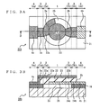
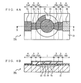
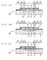
- Piezoelektrisches Element (20) umfassend:ein Substrat (21);eine untere Elektrodenschicht (24), welche auf oder über das Substrat geschichtet ist;eine piezoelektrische Schicht (22), welche auf oder über die untere Elektrodenschicht geschichtet ist;eine obere Elektrodenschicht (23), welche auf oder über die piezoelektrische Schicht geschichtet ist;einen Ausnehmungsabschnitt (25), welcher unter einem die untere Elektrodenschicht, die piezoelektrische Schicht und die obere Elektrodenschicht enthaltenden piezoelektrischen Vibrationsabschnitt (1) gebildet ist; undzumindest zwei Brückenabschnitte (2a, 2b), welche sich von einem Außenabschnitt des piezoelektrischen Vibrationsabschnitts erstrecken, um den piezoelektrischen Vibrationsabschnitt oberhalb des Ausnehmungsabschnitts am Substrat abzustützen,wobei die zumindest zwei Brückenabschnitte nicht achsensymmetrisch bezüglich irgendeines den piezoelektrischen Vibrationsabschnitt durchlaufenden Liniensegments und nicht punktsymmetrisch bezüglich irgendeines Punkts im piezoelektrischen Vibrationsabschnitt in einer Projektion des piezoelektrischen Vibrationsabschnitts in der Schichtungsrichtung sind.
- Piezoelektrisches Element nach Anspruch 1, wobei der Ausnehmungsabschnitt durch Bearbeitung des Substrats gebildet ist.
- Piezoelektrisches Element nach Anspruch 1, wobei der Ausnehmungsabschnitt durch Bearbeitung einer den Ausnehmungsabschnitt bildenden Schicht (10) zum Bilden des auf dem Substrat vorgesehenen Ausnehmungsabschnitts gebildet ist.
- Piezoelektrisches Element nach Anspruch 1, des Weiteren umfassend eine dielektrische Schicht (7a, 7b, 7c), welche so vorgesehen ist, dass sie in Kontakt mit zumindest einer Schicht ist, welche aus der Gruppe, bestehend aus der unteren Elektrodenschicht, der piezoelektrischen Schicht und der oberen Elektrodenschicht, ausgewählt ist.
- Piezoelektrisches Element nach Anspruch 4, wobei die dielektrische Schicht (7a) zwischen dem Substrat und der unteren Elektrodenschicht vorgesehen ist.
- Piezoelektrisches Element nach Anspruch 4, wobei die Brückenabschnitte gebildet sind durch Erstrecken wenigstens einer Schicht, welche aus der Gruppe, bestehend aus der unteren Elektrodenschicht, der piezoelektrischen Schicht, der oberen Elektrodenschicht und der dielektrischen Schicht, ausgewählt ist.
- Piezoelektrisches Element nach Anspruch 4, wobei wenigstens eine Schicht, ausgewählt aus der Gruppe, bestehend aus der unteren Elektrodenschicht, der piezoelektrischen Schicht, der oberen Elektrodenschicht und der dielektrischen Schicht, so ausgebildet ist, dass sie sich zumindest bis zu einem Abschnitt eines Außenabschnitts des Ausnehmungsabschnitts erstreckt.
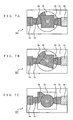
- Piezoelektrisches Element nach Anspruch 1, wobei die zumindest zwei Brückenabschnitte umfassen:einen ersten Brückenabschnitt (2a), welcher einen sich von der oberen Elektrodenschicht erstreckenden Abschnitt enthält; undeinen zweiten Brückenabschnitt (2b), welcher einen sich von der unteren Elektrodenschicht erstreckenden Abschnitt enthält; unddas piezoelektrische Element des Weiteren umfasst:eine erste Beschaltungselektrode (3a), welche in einem Außenabschnitt des Ausnehmungsabschnitts auf oder oberhalb des Substrats so vorgesehen ist, dass sie elektrisch mit dem von der oberen Elektrodenschicht sich erstreckenden Abschnitt verbunden ist und dass sie mit einer ersten Anschlusselektrode verbunden ist, undeine zweite Beschaltungselektrode (3b), welche in einem Außenabschnitt des Ausnehmungsabschnitts auf oder oberhalb des Substrats so vorgesehen ist, dass sie elektrisch mit dem von der unteren Elektrodenschicht sich erstreckenden Abschnitt verbunden ist und dass sie mit einer zweiten Anschlusselektrode verbunden ist.
- Piezoelektrisches Element nach Anspruch 8, wobei
die erste Beschaltungselektrode so vorgesehen ist, dass sich eine Zentrallinie (OMa), welche den Mittelpunkt des piezoelektrischen Vibrationsabschnitts und den Mittelpunkt des ersten Brückenabschnitts verbindet, nicht mit einer zweiten Zentrallinie (OM1) überlappt, welche den Mittelpunkt des piezoelektrischen Vibrationsabschnitts und den Mittelpunkt der ersten Beschaltungselektrode in einer Projektion in der Schichtungsrichtung verbindet, und
die zweite Beschaltungselektrode so vorgesehen ist, dass eine dritte Zentrallinie (OMb), welche den Mittelpunkt des piezoelektrischen Vibrationsabschnitts und den Mittelpunkt des zweiten Brückenabschnitts verbindet, nicht mit einer vierten Zentrallinie (OM2) überlappt, welche den Mittelpunkt des piezoelektrischen Vibrationsabschnitts und den Mittelpunkt der zweiten Beschaltungselektrode in einer Projektion in Schichtungsrichtung verbindet. - Piezoelektrisches Element nach Anspruch 9, wobei
der erste Brückenabschnitt so vorgesehen ist, dass der erste Brückenabschnitt nicht zwischen dem piezoelektrischen Vibrationsabschnitt und der ersten Beschaltungselektrode in der Schichtungsrichtung vorgesehen ist, und
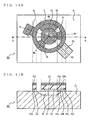
der zweiten Brückenabschnitt so vorgesehen ist, dass der zweite Brückenabschnitt nicht zwischen dem piezoelektrischen Vibrationsabschnitt und der zweiten Beschaltungselektrode in der Schichtungsrichtung vorgesehen ist. - Piezoelektrisches Element nach Anspruch 1, des Weiteren umfassend:eine erste Relais-Elektrode (5a), welche elektrisch mit der sich bis zu einem Umfang des Ausnehmungsabschnitts via der zumindest zwei Brückenabschnitte erstreckenden oberen Elektrodenschicht verbunden ist; undeine zweite Relais-Elektrode (5b), welche elektrisch mit der sich bis zu einem Umfang des Ausnehmungsabschnitts via der zumindest zwei Brückenabschnitte erstreckenden unteren Elektrodenschicht verbunden ist.
- Piezoelektrisches Element nach Anspruch 11, wobei zumindest eine der ersten Relais-Elektrode und der zweiten Relais-Elektrode in einer Ringform oder in einer Rahmenform entlang des Umfangs des Ausnehmungsabschnitts vorgesehen ist.
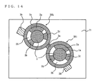
- Komposit-piezoelektrisches Element (20j), bei dem zumindest zwei piezoelektrische Elemente elektrisch miteinander verbunden sind, wobei zumindest eines der piezoelektrischen Elemente (20k, 201) wie in Anspruch 1 ist.
- Piezoelektrisches Element (100) umfassend:ein Substrat (107);eine untere Elektrodenschicht (103), welche auf oder über das Substrat geschichtet ist;eine piezoelektrische Schicht (102), welche auf oder über die untere Elektrodenschicht geschichtet ist;eine obere Elektrodenschicht (101), welche auf oder über die piezoelektrische Schicht geschichtet ist;eine Spiegelschicht (104), welche unter einem piezoelektrischen Vibrationsabschnitt gebildet ist, welcher die untere Elektrodenschicht, die piezoelektrische Schicht und die obere Elektrodenschicht enthält;einen ersten Verbindungsabschnitt, welcher einen sich von der oberen Elektrodenschicht erstreckenden Abschnitt zur elektrischen und mechanischen Verbindung mit einer auf der Spiegelschicht gebildeten ersten Beschaltungselektrode enthält; undeinen zweiten Verbindungsabschnitt, welcher einen sich von der unteren Elektrodenschicht erstreckenden Abschnitt zur elektrischen und mechanischen Verbindung mit einer auf der Spiegelschicht gebildeten zweiten Beschaltungselektrode enthält,wobei der erste Verbindungsabschnitt und der zweite Verbindungsabschnitt so geformt sind, dass sie nicht achsensymmetrisch bezüglich irgendeines den piezoelektrischen Vibrationsabschnitt durchlaufenden Liniensegments ist und dass sie nicht punktsymmetrisch bezüglich irgendeines Punkts im piezoelektrischen Vibrationsabschnitt in einer Projektion des piezoelektrischen Vibrationsabschnitts in der Schichtungsrichtung ist.
- Filter umfassend eine Mehrzahl piezoelektrischer Elemente, wobei zumindest eines der piezoelektrischen Elemente wie in Anspruch 1 ist.
- Duplexer (200) umfassend einen Filter mit einer Mehrzahl piezoelektrischer Elemente, wobei zumindest eines der piezoelektrischen Elemente wie in Anspruch 1 ist.
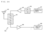
- Kommunikationsausrüstung (411) umfassend ein piezoelektrisches Element, wobei das piezoelektrische Element wie in Anspruch 1 ist.
Applications Claiming Priority (2)
| Application Number | Priority Date | Filing Date | Title |
|---|---|---|---|
| JP2003390519 | 2003-11-20 | ||
| JP2003390519 | 2003-11-20 |
Publications (3)
| Publication Number | Publication Date |
|---|---|
| EP1533896A2 EP1533896A2 (de) | 2005-05-25 |
| EP1533896A3 EP1533896A3 (de) | 2006-09-13 |
| EP1533896B1 true EP1533896B1 (de) | 2011-11-02 |
Family
ID=34431593
Family Applications (1)
| Application Number | Title | Priority Date | Filing Date |
|---|---|---|---|
| EP04027275A Expired - Fee Related EP1533896B1 (de) | 2003-11-20 | 2004-11-17 | Piezoelektrisches Element als solches sowie in Zusammensetzung, in einem Filter, in einem Duplexer oder in Kommunikationsvorrichtung |
Country Status (3)
| Country | Link |
|---|---|
| US (1) | US7224105B2 (de) |
| EP (1) | EP1533896B1 (de) |
| CN (1) | CN100420056C (de) |
Cited By (1)
| Publication number | Priority date | Publication date | Assignee | Title |
|---|---|---|---|---|
| WO2020214681A1 (en) * | 2019-04-19 | 2020-10-22 | Akoustis, Inc. | Baw resonators with antisymmetric thick electrodes |
Families Citing this family (24)
| Publication number | Priority date | Publication date | Assignee | Title |
|---|---|---|---|---|
| US7126255B2 (en) * | 2004-04-05 | 2006-10-24 | Ngk Insulators, Ltd. | Piezoelectric/electrostrictive film-type device |
| JP2006020020A (ja) * | 2004-07-01 | 2006-01-19 | Nippon Dempa Kogyo Co Ltd | 水晶振動子 |
| JP4535841B2 (ja) * | 2004-10-28 | 2010-09-01 | 富士通メディアデバイス株式会社 | 圧電薄膜共振子及びこれを用いたフィルタ |
| JP4149444B2 (ja) * | 2005-01-12 | 2008-09-10 | 富士通メディアデバイス株式会社 | 圧電薄膜共振子及びこれを用いたフィルタ |
| JP4550658B2 (ja) * | 2005-04-28 | 2010-09-22 | 富士通メディアデバイス株式会社 | 圧電薄膜共振器およびフィルタ |
| JP4476903B2 (ja) * | 2005-08-24 | 2010-06-09 | 株式会社東芝 | 薄膜圧電共振器およびフィルタ回路 |
| JP4707533B2 (ja) | 2005-10-27 | 2011-06-22 | 太陽誘電株式会社 | 圧電薄膜共振器およびフィルタ |
| US7538477B2 (en) * | 2006-11-27 | 2009-05-26 | Avago Technologies Wireless Ip (Singapore) Pte. Ltd. | Multi-layer transducers with annular contacts |
| US7579753B2 (en) * | 2006-11-27 | 2009-08-25 | Avago Technologies Wireless Ip (Singapore) Pte. Ltd. | Transducers with annular contacts |
| EP2140505B1 (de) * | 2007-03-21 | 2012-06-27 | The University of Vermont and State Agricultural | Piezoelektrische vibrationsenergiegewinnungssysteme mit energiegewinnung im parametrischen biegemodus |
| JP5191762B2 (ja) * | 2008-03-06 | 2013-05-08 | 太陽誘電株式会社 | 圧電薄膜共振器、フィルタ、および通信装置 |
| JP5220503B2 (ja) * | 2008-07-23 | 2013-06-26 | 太陽誘電株式会社 | 弾性波デバイス |
| US10129656B2 (en) * | 2009-01-30 | 2018-11-13 | Avago Technologies International Sales Pte. Limited | Active temperature control of piezoelectric membrane-based micro-electromechanical devices |
| US9327316B2 (en) * | 2009-06-30 | 2016-05-03 | Avago Technologies General Ip (Singapore) Pte. Ltd. | Multi-frequency acoustic array |
| US8258678B2 (en) * | 2010-02-23 | 2012-09-04 | Avago Technologies Wireless Ip (Singapore) Pte. Ltd. | Short range ultrasonic device with broadbeam ultrasonic transducers |
| US9000656B2 (en) * | 2011-03-15 | 2015-04-07 | Qualcomm Mems Technologies, Inc. | Microelectromechanical system device including a metal proof mass and a piezoelectric component |
| KR101856060B1 (ko) | 2011-12-01 | 2018-05-10 | 삼성전자주식회사 | 체적 음향 공진기 |
| JP6617504B2 (ja) * | 2015-10-02 | 2019-12-11 | セイコーエプソン株式会社 | 圧電素子、プローブ及び超音波測定装置 |
| DE102016103834B4 (de) * | 2016-03-03 | 2018-12-06 | Snaptrack, Inc. | BAW-Vorrichtung |
| CN107181472B (zh) * | 2016-03-10 | 2020-11-03 | 中芯国际集成电路制造(上海)有限公司 | 薄膜体声波谐振器、半导体器件及其制造方法 |
| CN107181470B (zh) * | 2016-03-10 | 2020-10-02 | 中芯国际集成电路制造(上海)有限公司 | 薄膜体声波谐振器、半导体器件及其制造方法 |
| KR102052795B1 (ko) | 2017-03-23 | 2019-12-09 | 삼성전기주식회사 | 음향 공진기 |
| CN109301061A (zh) * | 2018-09-28 | 2019-02-01 | 天津大学 | 柔性微型压电超声换能器、阵列及其形成方法 |
| CN114826196B (zh) * | 2022-05-05 | 2023-11-03 | 武汉敏声新技术有限公司 | 一种可调谐的薄膜体声波谐振器及其制备方法 |
Family Cites Families (11)
| Publication number | Priority date | Publication date | Assignee | Title |
|---|---|---|---|---|
| US3382381A (en) | 1965-05-27 | 1968-05-07 | Piezo Technology Inc | Tab plateback |
| US3980911A (en) * | 1974-02-11 | 1976-09-14 | Cts Corporation | Support structure and housing for piezoelectric crystal |
| IT1078411B (it) * | 1977-04-08 | 1985-05-08 | Telettra Lab Telefon | Risuonatori a quarzo |
| GB2146839B (en) * | 1983-07-27 | 1987-04-01 | Nihon Dempa Kogyo Co | Piezoelectric resonator |
| JPH09130199A (ja) | 1995-10-27 | 1997-05-16 | Mitsubishi Electric Corp | 圧電薄膜素子およびその製法 |
| US6271619B1 (en) | 1997-05-13 | 2001-08-07 | Mitsubishi Denki Kabushiki Kaisha | Piezoelectric thin film device |
| JP3551078B2 (ja) * | 1999-05-12 | 2004-08-04 | 松下電器産業株式会社 | 積層型圧電トランスとこれを用いた電子機器 |
| JP2001244778A (ja) * | 1999-12-22 | 2001-09-07 | Toyo Commun Equip Co Ltd | 高周波圧電振動子 |
| EP1170862B1 (de) | 2000-06-23 | 2012-10-10 | Murata Manufacturing Co., Ltd. | Piezoelektrischer Resonator und diesen enthaltendes piezoelektrisches Filter |
| US6714102B2 (en) | 2001-03-01 | 2004-03-30 | Agilent Technologies, Inc. | Method of fabricating thin film bulk acoustic resonator (FBAR) and FBAR structure embodying the method |
| KR100616508B1 (ko) | 2002-04-11 | 2006-08-29 | 삼성전기주식회사 | Fbar 소자 및 그 제조방법 |
-
2004
- 2004-11-17 EP EP04027275A patent/EP1533896B1/de not_active Expired - Fee Related
- 2004-11-18 US US10/990,435 patent/US7224105B2/en not_active Expired - Fee Related
- 2004-11-19 CN CNB2004100956740A patent/CN100420056C/zh not_active Expired - Fee Related
Cited By (3)
| Publication number | Priority date | Publication date | Assignee | Title |
|---|---|---|---|---|
| WO2020214681A1 (en) * | 2019-04-19 | 2020-10-22 | Akoustis, Inc. | Baw resonators with antisymmetric thick electrodes |
| US10879872B2 (en) | 2019-04-19 | 2020-12-29 | Akoustis, Inc. | BAW resonators with antisymmetric thick electrodes |
| US11695390B2 (en) | 2019-04-19 | 2023-07-04 | Akoustis, Inc. | BAW resonators with antisymmetric thick electrodes |
Also Published As
| Publication number | Publication date |
|---|---|
| US7224105B2 (en) | 2007-05-29 |
| EP1533896A2 (de) | 2005-05-25 |
| EP1533896A3 (de) | 2006-09-13 |
| CN1645640A (zh) | 2005-07-27 |
| US20050110369A1 (en) | 2005-05-26 |
| CN100420056C (zh) | 2008-09-17 |
Similar Documents
| Publication | Publication Date | Title |
|---|---|---|
| EP1533896B1 (de) | Piezoelektrisches Element als solches sowie in Zusammensetzung, in einem Filter, in einem Duplexer oder in Kommunikationsvorrichtung | |
| US7378922B2 (en) | Piezoelectric filter | |
| CN100539413C (zh) | 弹性表面波元件、弹性表面波装置以及通信装置 | |
| JP3969224B2 (ja) | 圧電共振子及びそれを用いた圧電フィルタ・デュプレクサ・通信装置 | |
| US9197189B2 (en) | Acoustic wave device | |
| US6437484B1 (en) | Piezoelectric resonator | |
| JP5792554B2 (ja) | 弾性波デバイス | |
| EP1826901B1 (de) | Dünnfilm-biegewellenresonator | |
| US7148604B2 (en) | Piezoelectric resonator and electronic component provided therewith | |
| JP2005057332A (ja) | フィルタ装置およびそれを用いた分波器 | |
| JP2002268644A (ja) | モノリシックfbarデュプレクサおよびそれを作製する方法 | |
| JP4791181B2 (ja) | 薄膜バルク音響波共振子、それを備えるフィルタおよび通信装置ならびに薄膜バルク音響波共振子の製造方法 | |
| JP6427075B2 (ja) | 弾性波デバイス、分波器、及びモジュール | |
| CN104660211A (zh) | 声波滤波器和双工器 | |
| JP6538007B2 (ja) | 弾性波デバイス | |
| US20040227587A1 (en) | Filter device capable of obtaining attenuation characteristic of sharpness in narrow band width and branching filter using the same | |
| CN1619958B (zh) | 使用压电谐振器的滤波器 | |
| JP4836748B2 (ja) | バルク音響波共振子及びフィルタ装置並びに通信装置 | |
| WO2018070369A1 (ja) | 弾性波装置 | |
| EP1274168B1 (de) | Piezoelektrischer Resonator, piezoelektrisches Filter, entsprechende Herstellungsverfahren, Duplexer und elektronisches Kommunikationsgerät | |
| JP4554337B2 (ja) | 圧電素子、および複合圧電素子、ならびにそれらを用いたフィルタ、共用器、通信機器 | |
| JP5184179B2 (ja) | 薄膜共振子、フィルタおよびデュプレクサ | |
| US11264968B2 (en) | High-frequency device and multiplexer | |
| JP5207902B2 (ja) | バルク音響波共振子および電子部品 | |
| US10972067B2 (en) | Filter and multiplexer |
Legal Events
| Date | Code | Title | Description |
|---|---|---|---|
| PUAI | Public reference made under article 153(3) epc to a published international application that has entered the european phase |
Free format text: ORIGINAL CODE: 0009012 |
|
| AK | Designated contracting states |
Kind code of ref document: A2 Designated state(s): AT BE BG CH CY CZ DE DK EE ES FI FR GB GR HU IE IS IT LI LU MC NL PL PT RO SE SI SK TR |
|
| AX | Request for extension of the european patent |
Extension state: AL HR LT LV MK YU |
|
| PUAL | Search report despatched |
Free format text: ORIGINAL CODE: 0009013 |
|
| AK | Designated contracting states |
Kind code of ref document: A3 Designated state(s): AT BE BG CH CY CZ DE DK EE ES FI FR GB GR HU IE IS IT LI LU MC NL PL PT RO SE SI SK TR |
|
| AX | Request for extension of the european patent |
Extension state: AL HR LT LV MK YU |
|
| 17P | Request for examination filed |
Effective date: 20061115 |
|
| AKX | Designation fees paid |
Designated state(s): DE FR GB |
|
| RAP1 | Party data changed (applicant data changed or rights of an application transferred) |
Owner name: PANASONIC CORPORATION |
|
| 17Q | First examination report despatched |
Effective date: 20101008 |
|
| GRAP | Despatch of communication of intention to grant a patent |
Free format text: ORIGINAL CODE: EPIDOSNIGR1 |
|
| GRAS | Grant fee paid |
Free format text: ORIGINAL CODE: EPIDOSNIGR3 |
|
| GRAA | (expected) grant |
Free format text: ORIGINAL CODE: 0009210 |
|
| AK | Designated contracting states |
Kind code of ref document: B1 Designated state(s): DE FR GB |
|
| REG | Reference to a national code |
Ref country code: GB Ref legal event code: FG4D |
|
| REG | Reference to a national code |
Ref country code: DE Ref legal event code: R096 Ref document number: 602004035084 Country of ref document: DE Effective date: 20120105 |
|
| PLBE | No opposition filed within time limit |
Free format text: ORIGINAL CODE: 0009261 |
|
| STAA | Information on the status of an ep patent application or granted ep patent |
Free format text: STATUS: NO OPPOSITION FILED WITHIN TIME LIMIT |
|
| REG | Reference to a national code |
Ref country code: FR Ref legal event code: ST Effective date: 20120817 |
|
| 26N | No opposition filed |
Effective date: 20120803 |
|
| GBPC | Gb: european patent ceased through non-payment of renewal fee |
Effective date: 20120202 |
|
| REG | Reference to a national code |
Ref country code: DE Ref legal event code: R097 Ref document number: 602004035084 Country of ref document: DE Effective date: 20120803 |
|
| PG25 | Lapsed in a contracting state [announced via postgrant information from national office to epo] |
Ref country code: GB Free format text: LAPSE BECAUSE OF NON-PAYMENT OF DUE FEES Effective date: 20120202 |
|
| PG25 | Lapsed in a contracting state [announced via postgrant information from national office to epo] |
Ref country code: FR Free format text: LAPSE BECAUSE OF NON-PAYMENT OF DUE FEES Effective date: 20120102 |
|
| PGFP | Annual fee paid to national office [announced via postgrant information from national office to epo] |
Ref country code: DE Payment date: 20131121 Year of fee payment: 10 |
|
| REG | Reference to a national code |
Ref country code: DE Ref legal event code: R119 Ref document number: 602004035084 Country of ref document: DE |
|
| PG25 | Lapsed in a contracting state [announced via postgrant information from national office to epo] |
Ref country code: DE Free format text: LAPSE BECAUSE OF NON-PAYMENT OF DUE FEES Effective date: 20150602 |