EP1531452A1 - Circuit d'attaque de pixel à multiplexage temporel de sous-pixels dans un affichage couleur à OLED - Google Patents
Circuit d'attaque de pixel à multiplexage temporel de sous-pixels dans un affichage couleur à OLED Download PDFInfo
- Publication number
- EP1531452A1 EP1531452A1 EP04090400A EP04090400A EP1531452A1 EP 1531452 A1 EP1531452 A1 EP 1531452A1 EP 04090400 A EP04090400 A EP 04090400A EP 04090400 A EP04090400 A EP 04090400A EP 1531452 A1 EP1531452 A1 EP 1531452A1
- Authority
- EP
- European Patent Office
- Prior art keywords
- green
- red
- blue
- time
- devices
- Prior art date
- Legal status (The legal status is an assumption and is not a legal conclusion. Google has not performed a legal analysis and makes no representation as to the accuracy of the status listed.)
- Granted
Links
- 239000003086 colorant Substances 0.000 claims abstract description 21
- 239000010409 thin film Substances 0.000 claims description 104
- 239000003990 capacitor Substances 0.000 claims description 22
- 238000000034 method Methods 0.000 claims description 14
- 230000004044 response Effects 0.000 claims description 3
- 102100036285 25-hydroxyvitamin D-1 alpha hydroxylase, mitochondrial Human genes 0.000 description 11
- 101000875403 Homo sapiens 25-hydroxyvitamin D-1 alpha hydroxylase, mitochondrial Proteins 0.000 description 11
- 238000010586 diagram Methods 0.000 description 11
- 239000011159 matrix material Substances 0.000 description 5
- 230000009467 reduction Effects 0.000 description 3
- 101100248200 Arabidopsis thaliana RGGB gene Proteins 0.000 description 1
- 101100122010 Methanocella arvoryzae (strain DSM 22066 / NBRC 105507 / MRE50) glmM gene Proteins 0.000 description 1
- 101100175002 Oryza sativa subsp. indica RGBB gene Proteins 0.000 description 1
- 101150049281 PRM1 gene Proteins 0.000 description 1
- 230000008901 benefit Effects 0.000 description 1
- 230000003247 decreasing effect Effects 0.000 description 1
- 230000007547 defect Effects 0.000 description 1
- 239000004973 liquid crystal related substance Substances 0.000 description 1
- 230000008569 process Effects 0.000 description 1
- 238000004904 shortening Methods 0.000 description 1
Images


Classifications
-
- G—PHYSICS
- G09—EDUCATION; CRYPTOGRAPHY; DISPLAY; ADVERTISING; SEALS
- G09G—ARRANGEMENTS OR CIRCUITS FOR CONTROL OF INDICATING DEVICES USING STATIC MEANS TO PRESENT VARIABLE INFORMATION
- G09G3/00—Control arrangements or circuits, of interest only in connection with visual indicators other than cathode-ray tubes
- G09G3/20—Control arrangements or circuits, of interest only in connection with visual indicators other than cathode-ray tubes for presentation of an assembly of a number of characters, e.g. a page, by composing the assembly by combination of individual elements arranged in a matrix no fixed position being assigned to or needed to be assigned to the individual characters or partial characters
- G09G3/22—Control arrangements or circuits, of interest only in connection with visual indicators other than cathode-ray tubes for presentation of an assembly of a number of characters, e.g. a page, by composing the assembly by combination of individual elements arranged in a matrix no fixed position being assigned to or needed to be assigned to the individual characters or partial characters using controlled light sources
- G09G3/30—Control arrangements or circuits, of interest only in connection with visual indicators other than cathode-ray tubes for presentation of an assembly of a number of characters, e.g. a page, by composing the assembly by combination of individual elements arranged in a matrix no fixed position being assigned to or needed to be assigned to the individual characters or partial characters using controlled light sources using electroluminescent panels
- G09G3/32—Control arrangements or circuits, of interest only in connection with visual indicators other than cathode-ray tubes for presentation of an assembly of a number of characters, e.g. a page, by composing the assembly by combination of individual elements arranged in a matrix no fixed position being assigned to or needed to be assigned to the individual characters or partial characters using controlled light sources using electroluminescent panels semiconductive, e.g. using light-emitting diodes [LED]
- G09G3/3208—Control arrangements or circuits, of interest only in connection with visual indicators other than cathode-ray tubes for presentation of an assembly of a number of characters, e.g. a page, by composing the assembly by combination of individual elements arranged in a matrix no fixed position being assigned to or needed to be assigned to the individual characters or partial characters using controlled light sources using electroluminescent panels semiconductive, e.g. using light-emitting diodes [LED] organic, e.g. using organic light-emitting diodes [OLED]
- G09G3/3225—Control arrangements or circuits, of interest only in connection with visual indicators other than cathode-ray tubes for presentation of an assembly of a number of characters, e.g. a page, by composing the assembly by combination of individual elements arranged in a matrix no fixed position being assigned to or needed to be assigned to the individual characters or partial characters using controlled light sources using electroluminescent panels semiconductive, e.g. using light-emitting diodes [LED] organic, e.g. using organic light-emitting diodes [OLED] using an active matrix
- G09G3/3233—Control arrangements or circuits, of interest only in connection with visual indicators other than cathode-ray tubes for presentation of an assembly of a number of characters, e.g. a page, by composing the assembly by combination of individual elements arranged in a matrix no fixed position being assigned to or needed to be assigned to the individual characters or partial characters using controlled light sources using electroluminescent panels semiconductive, e.g. using light-emitting diodes [LED] organic, e.g. using organic light-emitting diodes [OLED] using an active matrix with pixel circuitry controlling the current through the light-emitting element
-
- G—PHYSICS
- G09—EDUCATION; CRYPTOGRAPHY; DISPLAY; ADVERTISING; SEALS
- G09G—ARRANGEMENTS OR CIRCUITS FOR CONTROL OF INDICATING DEVICES USING STATIC MEANS TO PRESENT VARIABLE INFORMATION
- G09G2300/00—Aspects of the constitution of display devices
- G09G2300/04—Structural and physical details of display devices
- G09G2300/0439—Pixel structures
- G09G2300/0452—Details of colour pixel setup, e.g. pixel composed of a red, a blue and two green components
-
- G—PHYSICS
- G09—EDUCATION; CRYPTOGRAPHY; DISPLAY; ADVERTISING; SEALS
- G09G—ARRANGEMENTS OR CIRCUITS FOR CONTROL OF INDICATING DEVICES USING STATIC MEANS TO PRESENT VARIABLE INFORMATION
- G09G2300/00—Aspects of the constitution of display devices
- G09G2300/08—Active matrix structure, i.e. with use of active elements, inclusive of non-linear two terminal elements, in the pixels together with light emitting or modulating elements
- G09G2300/0804—Sub-multiplexed active matrix panel, i.e. wherein one active driving circuit is used at pixel level for multiple image producing elements
-
- G—PHYSICS
- G09—EDUCATION; CRYPTOGRAPHY; DISPLAY; ADVERTISING; SEALS
- G09G—ARRANGEMENTS OR CIRCUITS FOR CONTROL OF INDICATING DEVICES USING STATIC MEANS TO PRESENT VARIABLE INFORMATION
- G09G2300/00—Aspects of the constitution of display devices
- G09G2300/08—Active matrix structure, i.e. with use of active elements, inclusive of non-linear two terminal elements, in the pixels together with light emitting or modulating elements
- G09G2300/0809—Several active elements per pixel in active matrix panels
- G09G2300/0814—Several active elements per pixel in active matrix panels used for selection purposes, e.g. logical AND for partial update
-
- G—PHYSICS
- G09—EDUCATION; CRYPTOGRAPHY; DISPLAY; ADVERTISING; SEALS
- G09G—ARRANGEMENTS OR CIRCUITS FOR CONTROL OF INDICATING DEVICES USING STATIC MEANS TO PRESENT VARIABLE INFORMATION
- G09G2300/00—Aspects of the constitution of display devices
- G09G2300/08—Active matrix structure, i.e. with use of active elements, inclusive of non-linear two terminal elements, in the pixels together with light emitting or modulating elements
- G09G2300/0809—Several active elements per pixel in active matrix panels
- G09G2300/0842—Several active elements per pixel in active matrix panels forming a memory circuit, e.g. a dynamic memory with one capacitor
- G09G2300/0861—Several active elements per pixel in active matrix panels forming a memory circuit, e.g. a dynamic memory with one capacitor with additional control of the display period without amending the charge stored in a pixel memory, e.g. by means of additional select electrodes
-
- G—PHYSICS
- G09—EDUCATION; CRYPTOGRAPHY; DISPLAY; ADVERTISING; SEALS
- G09G—ARRANGEMENTS OR CIRCUITS FOR CONTROL OF INDICATING DEVICES USING STATIC MEANS TO PRESENT VARIABLE INFORMATION
- G09G2310/00—Command of the display device
- G09G2310/02—Addressing, scanning or driving the display screen or processing steps related thereto
- G09G2310/0235—Field-sequential colour display
-
- G—PHYSICS
- G09—EDUCATION; CRYPTOGRAPHY; DISPLAY; ADVERTISING; SEALS
- G09G—ARRANGEMENTS OR CIRCUITS FOR CONTROL OF INDICATING DEVICES USING STATIC MEANS TO PRESENT VARIABLE INFORMATION
- G09G2320/00—Control of display operating conditions
- G09G2320/06—Adjustment of display parameters
- G09G2320/0606—Manual adjustment
-
- G—PHYSICS
- G09—EDUCATION; CRYPTOGRAPHY; DISPLAY; ADVERTISING; SEALS
- G09G—ARRANGEMENTS OR CIRCUITS FOR CONTROL OF INDICATING DEVICES USING STATIC MEANS TO PRESENT VARIABLE INFORMATION
- G09G2320/00—Control of display operating conditions
- G09G2320/06—Adjustment of display parameters
- G09G2320/0666—Adjustment of display parameters for control of colour parameters, e.g. colour temperature
Definitions
- the present invention relates to a self-emissive organic display device, and more particularly, to a time-divisional driving type organic electroluminescent display device in which red, green and blue light emitting elements are time-divisionally driven by one driving element and a driving method of the time-divisional driving type organic electroluminescent display device.
- Liquid crystal display (LCD) device and organic electroluminescent display device are often used in portable information appliances due to their lightweight and thin characteristics.
- the organic electroluminescent display device is being noticed as the next generation flat panel display device as the organic electroluminescent display device has better luminance and viewing angle characteristics compared to the LCD device.
- one pixel of an active matrix organic electroluminescent display device includes red, green and blue unit pixels, wherein each red, green and blue unit pixel is equipped with an electroluminescent (EL) device.
- Red, green and blue organic emitting layers are respectively interposed between anode electrode and cathode electrode in each EL device so that light is emitted from the red, green and blue organic emitting layers by a voltage applied to the anode electrode and cathode electrode.
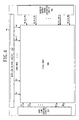
- FIG. 1 illustrates structure of a conventional active matrix organic electroluminescent display device.
- a conventional active matrix organic electroluminescent display device 10 includes a pixel part 100, a gate line driving circuit 110, a data line driving circuit 120 and a control part (not illustrated in FIG. 1).
- the pixel part 100 includes a plurality of gate lines 111 ⁇ 11m for providing scan signals S1 ⁇ Sm from the gate line driving circuit 110, a plurality of data lines 121 ⁇ 12n for providing data signals DR1, DG1, DB1 ⁇ DRn, DGn, DBn from the data line driving circuit 120 and a plurality of power supply lines 131 ⁇ 13n for providing power supply voltage VDD1 ⁇ VDDn.
- the pixel part 100 includes a plurality of pixels P11 ⁇ Pmn arranged in a matrix format and connected to the plurality of gate lines 111 ⁇ 11m, the plurality of data lines 121 ⁇ 12n and the plurality of power supply lines 131 ⁇ 13n.
- Each of the pixels P11 ⁇ Pmn includes three unit pixels, i.e., corresponding ones of red, green and blue unit pixels PR11 ⁇ PRmn, PG11 ⁇ PGmn, PB11 ⁇ PBmn, so that each of the red, green and blue unit pixels PR11 ⁇ PRmn, PG11 ⁇ PGmn, PB11 ⁇ PBmn is connected to a corresponding one of the gate lines, a corresponding one of the data lines and a corresponding one of the power supply lines.
- a pixel P11 includes a red unit pixel PR11, a green unit pixel PG11 and a blue unit pixel PB11, and is connected to a first gate line 111 for providing a first scan signal S1, a first data line 121 and a first power supply line 131.
- the red unit pixel PR11 of the pixel P11 is connected to the first gate line 111, an R data line 121R for providing an R data signal DR1 and an R power supply line 131R.
- the green unit pixel PG11 is connected to the first gate line 111, a G data line 121G for providing a G data signal DG1 and a G power supply line 131G.
- the blue unit pixel PB11 is connected to the first gate line 111, a B data line 121B for providing a B data signal DB1 and a B power supply line 131B.
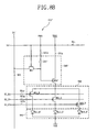
- FIG. 2 illustrates a pixel circuit P11 of a conventional organic electroluminescent display device.
- FIG. 2 illustrates a circuit diagram of the pixel P11 of FIG. 1, which includes red, green and blue unit pixels.
- the red unit pixel PR11 of the pixel P11 includes a switching transistor M1_R for which the scan signal S1 applied from the first gate line 111 is supplied to a gate, and the data signal DR1 is supplied to a source from the red data line 121R.
- the red unit pixel PR11 also includes a driving transistor M2_R for which a gate is connected to a drain of the switching transistor M1_R, and a power supply voltage VDD1 is supplied to a source from the power supply line 131R.
- the red unit pixel PR11 includes a capacitor C1_R connected between the gate and the source of the driving transistor M2_R, and a red EL device EL1_R having an anode connected to a drain of the driving transistor M2_R and a cathode connected to a ground voltage VSS.
- the green unit pixel PG11 includes a switching transistor M1_G for which the scan signal S1 applied from the first gate line 111 is supplied to a gate, and the data signal DG1 is supplied to a source from the green data line 121G.
- the green unit pixel PG11 also includes a driving transistor M2_G for which a gate is connected to a drain of the switching transistor M1_G, and the power supply voltage VDD1 is supplied to a source from the power supply line 131G.
- the green unit pixel PG11 includes a capacitor C1_G connected between the gate and the source of the driving transistor M2_G, and a green EL device EL1_G having an anode connected to a drain of the driving transistor M2_G and a cathode connected to a ground voltage VSS.
- the blue unit pixel PB11 includes a switching transistor M1_B for which the scan signal S1 applied from the first gate line 111 is supplied to a gate, and the data signal DB1 is supplied to a source from the blue data line 121B.
- the blue unit pixel PB11 also includes a driving transistor M2_B for which a gate is connected to a drain of the switching transistor M1_B, and the power supply voltage VDD1 is supplied to a source from the power supply line 131B.
- the blue unit pixel PB11 includes a capacitor C1_B connected between the gate and the source of the driving transistor M2_B, and a blue EL device EL1_B having an anode connected to a drain of the driving transistor M2_B and a cathode connected to a ground voltage VSS.
- the switching transistors M1_R, M1_G, M1_B of the red, green and blue unit pixels are driven, and red, green and blue data DR1, DG1, DB1 are applied to the gates of the driving transistors M2_R, M2_G, M2_B from the red, green and blue data lines 121 R, 121 G, 121 B, respectively, when the scan signal S1 is applied to the gate line 111.
- the driving transistors M2_R, M2_G, M2_B supply to the EL devices EL1_R, EL1_G, EL1_B a driving current corresponding to the difference between the data signals DR1, DG1, DB1 applied to the gate and the power supply voltage VDD1 respectively supplied from the red, green and blue power supply lines 131R, 131G, 131B.
- the driving current applied through the driving transistors M2_R, M2_G, M2_B to drive the pixel P11 drives the EL devices EL1_R, EL1_G, EL1_B.
- the capacitors C1_R, C1_G, C1_B store the data signals DR1, DG1, DB1 applied, respectively, to the red, green and blue data lines 121R, 121G, 121B.
- the first gate line 111 is driven, and pixels P11 ⁇ P1n connected to the first gate line 111 are driven when the scan signal S1 is applied to the first gate line 111.
- the switching transistors of the red, green and blue unit pixels PR11 ⁇ PR1n. PG11 ⁇ PG1n, PB11 ⁇ PB1n of the pixels P11 ⁇ P1n connected to the first gate line 111 are driven by the scan signal S1 applied to the first gate line 111.
- Red, green and blue data signals D(S1) (DR1 ⁇ DRn, DG1 ⁇ DGn, DB1 ⁇ DBn) are simultaneously applied to the gates of the driving transistors of the red, green and blue unit pixels, respectively, through the red, green and blue data lines 121R ⁇ 12nR, 121G ⁇ 12nG, 121B ⁇ 12nB composing first to n th data lines 121 ⁇ 12n according to the driving of the switching transistors.
- the driving transistors of the red, green and blue unit pixels supply a driving current corresponding to the red, green and blue data signals D(S1) (DR1 ⁇ DRn, DG1 ⁇ DGn, DB1 ⁇ DBn) applied to the red, green and blue data lines 121R ⁇ 12nR, 121G ⁇ 12nG, 121B ⁇ 12nB, respectively, to the red, green and blue EL devices. Therefore, the EL devices of the red, green and blue unit pixels PR11 ⁇ PR1n, PG11 ⁇ PG1n, PB11 ⁇ PB1n of the pixels P11 ⁇ P1n connected to the first gate line 111 are simultaneously driven when the scan signal S1 is applied to the first gate line 111.
- data signals D(S2)(DR1 ⁇ DRn, DG1 ⁇ DGn, DB1 ⁇ DBn) are applied to red, green and blue unit pixels PR21 ⁇ PR2n, PG21 ⁇ PG2n, PB21 ⁇ PB2n of pixels P21 ⁇ P2n connected to the second gate line 112 through red, green and blue data lines 121R ⁇ 12nR, 121G ⁇ 12nG, 121B ⁇ 12nB composing first to n th data lines 121 ⁇ 12n.
- EL devices of the red, green and blue unit pixels PR21 ⁇ PR2n, PG21 ⁇ PG2n, PB21 ⁇ PB2n of the pixels P21 ⁇ P2n connected to the second gate line 112 are simultaneously driven by a driving current corresponding to the data signals D(S2)(DR1 ⁇ DRn, DG1 ⁇ DGn, DB1 ⁇ DBn).
- EL devices of red, green and blue unit pixels PRm1 ⁇ PRmn, PGm1 ⁇ PGmn, PBm1 ⁇ PBmn of pixels Pm1 ⁇ Pmn connected to the m th gate line 11 m are simultaneously driven according to red, green and blue data signals D(Sm)(DR1 ⁇ DRn, DG1 ⁇ DGn, DB1 ⁇ DBn) applied to the red, green and blue data lines 121R ⁇ 12nR, 121G ⁇ 12nG, 121B ⁇ 12nB when a scan signal Sm is finally applied to m th gate line 11m by repeating the foregoing actions.
- an image is displayed by sequentially driving pixels (P11 ⁇ P1n) ⁇ (Pm1 ⁇ Pmn) connected to the respective gate lines 111 ⁇ 11m, thereby driving pixels during one frame when the scan signals S1 ⁇ Sm are sequentially applied starting with the first gate line 111 and ending with the m th gate line 11m.
- each pixel includes red, green and blue unit pixels, and driving elements for driving red, green and blue EL devices (i.e., a switching thin film transistor, a driving thin film transistor and a capacitor) are respectively arranged per the red, green and blue unit pixels. Further, data lines and power supply lines for supplying data signal and power supply ELVDD to each driving element are respectively arranged per the unit pixels.
- driving elements for driving red, green and blue EL devices i.e., a switching thin film transistor, a driving thin film transistor and a capacitor
- data lines and power supply lines for supplying data signal and power supply ELVDD to each driving element are respectively arranged per the unit pixels.
- three data lines and three power supply lines are arranged per pixel, and at least six transistors including three switching thin film transistors and three driving thin film transistors and at least three capacitors are required in each pixel.
- at least four signal lines are required per red, green and blue unit pixels as a separate emission control line for providing emission control signal is required in case that each pixel is controlled by emission control signals. Therefore, the circuit structure for the pixels in a conventional organic electroluminescent display device is complicated as a plurality of wirings and a plurality of elements are arranged per each pixel, and yield is reduced as probability of generating defects is increased accordingly.
- each pixel is reduced as the resolution of the display device is being increased, and not only is it difficult to arrange many elements on one pixel, but also the aperture ratio is reduced accordingly.
- a pixel circuit of an organic electroluminescent display device appropriate for high accuracy fineness and a driving method for the pixel circuit of the organic electroluminescent display device are provided.
- a pixel circuit of an organic electroluminescent display device capable of improving aperture ratio and yield and a driving method for the pixel circuit of the organic electroluminescent display device.
- a pixel circuit of an organic electroluminescent display device capable of preventing RC delay and voltage drop and a driving method for the pixel circuit of the organic electroluminescent display device.
- a pixel circuit of an organic electroluminescent display device capable of simplifying pixel structure and wiring by driving one pixel through one driving element and a driving method of the pixel circuit of the organic electroluminescent display device.
- a pixel circuit of a display device for realizing a certain color during a display period of time includes at least two light emitting elements, each said light emitting element for emitting a corresponding one of colors during the display period of time.
- An active element is commonly connected to the at least two light emitting elements to drive the at least two light emitting elements.
- the active element time-divisionally drives the at least two light emitting elements during the display period of time, such that one said light emitting element emits the corresponding one of the colors per a sub display period of time.
- the at least two light emitting elements realize the certain color in the display period of time by time-divisionally emitting the corresponding ones of the colors.
- the display period of time may be one frame, and the sub display period of time may be a sub frame.
- the one frame may be divided into at least three sub frames, and the at least two light emitting elements may be time-divisionally driven in accordance with at least two of the sub frames inside the one frame.
- One of the at least two light emitting elements may be driven again or the at least two light emitting elements may be simultaneously driven in a remaining at least one of the sub frames.
- the remaining at least one sub frame may be arbitrarily selected from the sub frames.
- a light emitting time of the at least two light emitting elements may be controlled to control white balance.
- the display device may be a FED (field emission display) or a PDP (plasma display panel).
- the at least two light emitting elements may include a red, green, blue or white EL device.
- a first electrode of the EL device may be connected to the active element, and a second electrode may be connected to a reference voltage(Vss).
- the EL device may be arranged in stripe type, delta type or mosaic type.
- the active element may include at least one switching element for driving the at least two light emitting elements.
- the at least one switching element may be a thin film transistor, a thin film diode, a diode or a TRS (triodic rectifier switch).
- a pixel circuit of a display device includes red, green and blue EL devices, at least one switching transistor for time-divisionally transmitting red, green and blue data signals, at least one driving transistor for time-divisionally driving the red, green and blue EL devices according to the red, green and blue data signals, and a storage element for storing the red, green and blue data signals.
- the red, green and blue EL devices are commonly connected to the at least one driving transistor, and time-divisionally emitted correspondingly to the red, green and blue data signals time-divisionally transmitted through the at least one driving transistor in response to red, green and blue emission control signals.
- a pixel circuit of an organic electroluminescent display device includes red, green and blue EL devices, a driving unit commonly connected to the red, green and blue EL devices to drive the red, green and blue EL devices, and a sequential control unit for time-divisionally controlling driving of the red, green and blue EL devices.
- the driving unit may include at least one switching transistor for switching data signals, at least one driving transistor for supplying driving current corresponding to the data signals to the red, green and blue EL devices, and a capacitor for storing the data signals.
- the driving unit may further include a threshold voltage compensation device for compensating a threshold voltage of the at least one driving transistor.
- a power supply voltage may be supplied to the at least one driving transistor and the capacitor through a common power supply line, or the power supply voltage may be supplied to the at least one driving transistor and the capacitor through separate power supply lines.
- the sequential control unit may include first, second and third control devices for time-divisionally controlling emission of the red, green and blue EL devices by controlling a supply of driving current to the red, green and blue EL devices from a driving transistor using corresponding red, green and blue emission control signals.
- the first, second and third control devices may include first, second and third thin film transistors in which the corresponding emission control signals are respectively applied to gates, sources are commonly connected to the driving unit, and drains are respectively connected to the red, green and blue EL devices.
- White balance may be controlled by controlling an active on time of the corresponding emission control signals applied to the sequential control unit, thereby controlling time in which driving current is applied to corresponding said EL devices by the first, second and third control devices.
- a pixel circuit of an organic electroluminescent display device includes a first thin film transistor having a gate connected to a gate line, and one of a source and a drain connected to a data line.
- a second thin film transistor has a gate connected to the other one of the source and the drain of the first thin film transistor, and one of a source and a drain connected to a power supply line.
- a capacitor is connected between the gate and said one of the source and the drain of the second thin film transistor.
- a third thin film transistor has one of a source and a drain connected to the other one of the source and the drain of the second thin film transistor, and a first emission control signal applied to a gate.
- a fourth thin film transistor has one of a source and a drain connected to the other one of the source and the drain of the second thin film transistor, and a second emission control signal applied to a gate.
- a fifth thin film transistor has one of a source and a drain connected to the other one of the source and the drain of the second thin film transistor, and a third emission control signal applied to a gate.
- Red, green and blue EL devices have first electrodes connected to the other ones of the source and the drain of the third, fourth and fifth thin film transistors, respectively, and second electrodes commonly grounded.
- a pixel circuit of a display device including a plurality of pixels realizes a certain color per display period of time.
- the pixel circuit includes at least two light emitting elements, each said light emitting element for emitting a corresponding one of colors during a sub display period of time in the certain section.
- the at least two light emitting elements are sequentially driven time-divisionally during the display period of time, such that each said light emitting element emits the corresponding one of the colors so that the pixel circuit realizes the certain color in the display period of time.
- a pixel circuit of a display device including a plurality of pixels realizes a certain color during a display period of time, and includes at least two light emitting elements, each said light emitting element for emitting one of corresponding colors during the display period of time, wherein the pixel circuit realizes the certain color during the display period of time by emitting one of the at least two light emitting elements for a sub display period of time so that the at least two light emitting elements time-divisionally emit the corresponding colors during the display period of time.
- a display device in yet another exemplary embodiment of the present invention, includes a plurality of pixels, each said pixel including red, green and blue EL devices, and at least one thin film transistor coupled to the red, green and blue EL devices to drive the red, green and blue EL devices.
- the red, green and blue EL devices of each said pixel include first electrodes commonly coupled to the at least one thin film transistor and second electrode commonly connected to a reference voltage(Vss).
- the red, green and blue EL devices are time-divisionally emitted by the at least one thin film transistor in each said pixel.
- a flat panel display device includes a plurality of gate lines, data lines and power supply lines, and a plurality of pixels, each said pixel connected to a corresponding said gate line, a corresponding said data line and a corresponding said power supply line.
- Each of the pixels includes red, green and blue EL devices, at least one thin film transistor commonly coupled to the red, green and blue EL devices to time-divisionally drive the red, green and blue EL devices, and red, green and blue emission controlling thin film transistors connected between the at least one thin film transistor and the red, green and blue EL devices, respectively, to control the red, green and blue EL devices so that the red, green and blue EL devices are time-divisionally emitted inside one frame including a plurality of sub frames, in accordance with the sub frames.
- a flat panel display device includes a plurality of gate lines, data lines and power supply lines; and a plurality of pixels. Each said pixel is connected to a corresponding said gate line, a corresponding said data line and a corresponding said power supply line.
- Each of the pixels includes a first thin film transistor having a gate connected to the corresponding said gate line, and one of a source and a drain connected to the corresponding said data line.
- a second thin film transistor has a gate connected to the other one of the source and the drain of the first thin film transistor, and one of a source and a drain connected to the corresponding said power supply line.
- a capacitor is connected between the gate and said one of the source and the drain of the second thin film transistor.
- a third thin film transistor has one of a source and a drain connected to the other one of the source and the drain of the second thin film transistor, and a first emission control signal applied to a gate.
- a fourth thin film transistor has one of a source and a drain connected to the other one of the source and the drain of the second thin film transistor, and a second emission control signal applied to a gate.
- a fifth thin film transistor has one of a source and a drain connected to the other one source and the drain of the second thin film transistor, and a third emission control signal applied to a gate.
- Red, green and blue EL devices have first electrodes connected to the other ones of the source and the drain of the third, fourth and fifth thin film transistors, respectively, and second electrodes commonly connected to a reference voltage(Vss).
- a flat panel display device includes a plurality of gate lines, data lines, emission control lines and power supply lines, and a pixel part including a plurality of pixels, each said pixel connected to a corresponding said gate line, a corresponding said data line, a corresponding said emission control line and a corresponding said power supply line.
- At least one gate line driving circuit supplies a plurality of scan signals to the gate lines.
- At least one data line driving circuit time-divisionally supplies red, green and blue data signals to the data lines.
- At least one emission control signal generating circuit supplies emission control signals to the emission control lines.
- Each of the pixels includes red, green and blue EL devices, at least one thin film transistor commonly coupled to the red, green and blue EL devices to time-divisionally drive the red, green and blue EL devices, and red, green and blue emission controlling thin film transistors connected between the at least one thin film transistor and the red, green and blue EL devices to control the red, green and blue EL devices so that the red, green and blue EL devices are time-divisionally emitted inside one frame including a plurality of sub frames, in accordance with the sub frames.
- a method for driving a flat panel display device including a plurality of gate lines, data lines and power supply lines, and a plurality of pixels, each said pixel connected to a corresponding said gate line, a corresponding said data line and a corresponding said power supply line.
- Each of the pixels includes at least red, green and blue EL devices. Red, green and blue data are time-divisionally supplied during a display period of time per a sub display period of time through a same data line in each said pixel so that red, green and blue EL devices are sequentially driven to realize a certain color in the display period of time.
- a method for driving a flat panel display device including a plurality of gate lines, data lines and power supply lines, and a plurality of pixels, each said pixel connected to a corresponding said gate line, a corresponding said data line and a corresponding said power supply line.
- Each of the pixels includes at least red, green and blue EL devices.
- a certain color is realized in a display period of time.
- Scan signals are generated at the corresponding said gate line per a sub display period of time in the display period of time.
- Red, green and blue data are time-divisionally applied to the corresponding said data line whenever the scan signals are generated so that red, green and blue driving currents are generated.
- Red, green and blue EL devices of pixels connected to the corresponding said gate line are time-divisionally driven by R, G and B emission control signals.
- FIG. 4 illustrates a block structural view of an organic electroluminescent display device according to a first exemplary embodiment of the present invention.
- an organic electroluminescent display device 50 includes a pixel part 500, a gate line driving circuit 510, a data line driving circuit 520 and an emission control signal generating circuit 590.
- the gate line driving circuit 510 sequentially generates scan signals S1' ⁇ Sm' to gate lines of the pixel part 500 during one frame.
- the data line driving circuit 520 sequentially supplies red, green and blue data signals D1' ⁇ Dn' to data lines of the pixel part 500 whenever scan signals are applied during one frame.
- the emission control signal generating circuit 590 sequentially supplies emission control signals EC_R, G, B1 ⁇ EC_R, G, Bm for controlling emission of red, green and blue EL devices to emission control lines 591 ⁇ 59m of the pixel part 500 whenever scan signals are applied during one frame.
- the EL devices may be arranged in stripe type, delta type or mosaic type.
- at least one of the gate line driving circuit 510, the data line driving circuit 520 and the emission control signal generating circuit may have a redundancy function.
- FIG. 5A illustrates one example of block structure of pixel part in an organic electroluminescent display device according to the first exemplary embodiment of the present invention.
- a pixel part 500' of an organic electroluminescent display device 50' includes a plurality of gate lines 511 ⁇ 51m to which scan signals S1' ⁇ Sm' are supplied from a gate line driving circuit 510, and a plurality of data lines 521 ⁇ 52n to which data signals D1' ⁇ Dn' are supplied from a data line driving circuit 520.
- the pixel part 500' also includes a plurality of emission control lines 591 ⁇ 59m to which emission control signals EC_R, G, B1 ⁇ EC_R, G, Bm are supplied from an emission control signal generating circuit 590, and a plurality of power supply lines 531 ⁇ 53n for supplying power supply voltage VDD1 ⁇ VDDn.
- the pixel part 500' further includes a plurality of pixels P11' ⁇ Pmn' arranged in a matrix format, and connected to the plurality of gate lines 511 ⁇ 51m, the plurality of data lines 521 ⁇ 52n, the plurality of emission control lines 591 ⁇ 59m and the plurality of power supply lines 531 ⁇ 53n.
- Each of the plurality of pixels P11' ⁇ Pmn' is connected to one corresponding gate line in the plurality of gate lines 511 ⁇ 51m, one corresponding data line in the plurality of data lines 521 ⁇ 52n, one corresponding emission control line in the plurality of emission control lines 591 ⁇ 59m and one corresponding power supply line in the plurality of power supply lines 531 ⁇ 53n.
- the pixel P11' is connected to the first gate line 511 for supplying the first scan signal S1', the first data line 521 for supplying the first data signal D1', the first emission control line 591 for supplying the first emission control signal EC_R, G, B1, and the first power supply line 531 for supplying the first power supply voltage VDD1.
- corresponding scan signals are applied to the pixels P11' ⁇ Pmn' through corresponding scan lines, and the corresponding red, green and blue data signals are sequentially supplied to the pixels P11' ⁇ Pmn' through corresponding data lines. Further, corresponding red, green and blue emission control signals are sequentially supplied to the pixels P11' ⁇ Pmn' through corresponding emission control lines, and corresponding power supply voltage is supplied to the pixels P11' ⁇ Pmn' through corresponding power supply lines.
- Each of the pixels indicates a certain color, such that an image is displayed during one frame by sequentially applying corresponding red, green and blue data signals to the pixels whenever corresponding scan signals are applied to the pixels and sequentially driving red, green and blue EL devices according to red, green and blue emission control signals, thereby sequentially emitting lights corresponding to the red, green and blue data signals.
- FIG. 6 schematically illustrates a pixel circuit for one pixel in a time-divisionally driving type organic electroluminescent display device according to the first exemplary embodiment of the present invention.
- FIG. 6 illustrates one pixel P11' in a plurality of pixels.
- the pixel includes an active element 570 connected to the first gate line 511, the first data line 521, the first emission control line 591 and the first common power supply line 531, and red, green and blue EL devices EL1_R', EL1_G', EL1_B' connected in parallel between the active element 570 and a common voltage (e. g., ground) VSS.
- First electrodes e.g., anode electrodes
- second electrodes e.g., cathode electrodes
- the red, green and blue EL devices EL1_R', EL1_G', EL1_B' should be time-divisionally driven so that a pixel P11' displays a certain color by driving the three red, green and blue EL devices EL1_R', EL1_G', EL1_B' during one frame since the red, green and blue EL devices EL1_R', EL1_G', EL1_B' share one active element 570 in a pixel circuit having the structure of FIG. 6.
- the red, green and blue EL devices EL1_R', EL1_G', EL1_B' are time-divisionally driven during one frame so that the pixel P11' realizes a certain color by dividing one frame into three sub frames and driving one of the red, green and blue EL devices EL1_R', EL1_G', EL1_B' during each sub frame.
- the active element 570 drives the red EL device EL1_R' using the emission control signal EC_R1 generated to the emission control line 591 from the emission control signal generating circuit 590 so that red color corresponding to red data is emitted if red data DR1' is applied as a data D1' applied to the data line 521 as the scan signal S1' is applied from the gate line 511 to the active element 570 in the first sub frame of one frame.
- green data DG1' is applied as the data D1' applied to the data line 521, and the green EL device EL1_G' is emitted by the emission control signal EC_G1 generated to the emission control line 591 from the emission control signal generating circuit 590 so that green color corresponding to the green data is emitted.
- blue data DB1' is applied as the data D1' applied to the data line 521, and the blue EL device EL1_B' is emitted by the emission control signal EC_B1 generated to the emission control line 591 from the emission control signal generating circuit 590 so that blue color corresponding to the blue data is emitted. Therefore, red, green and blue EL devices are sequentially driven time-divisionally during one frame so that each pixel emits a certain color to display an image.
- emission sequence of red, green and blue EL devices or red, green, blue and white EL devices may be temporarily or permanently changed, and/or one frame may be divided into more than three sub frames so that at least one color out of red, green and blue colors is further emitted in the remaining sub frame(s) in order to adjust chromaticity, brightness or luminance.
- one color of red, green, blue or white can be further emitted during an additional one sub frames such as RRGB, RGGB, RGBB and RGBW by dividing one frame into four sub frames, and the additional emitted color is emitted from an appropriate sub frame in a plurality of sub frames, wherein one EL device in the red, green, blue and white EL devices is driven, or at least two EL devices in the red, green, blue and white EL devices are driven so that one color of red, green, blue or white is further emitted during the additional one or more sub frames.
- an additional one sub frames such as RRGB, RGGB, RGBB and RGBW by dividing one frame into four sub frames, and the additional emitted color is emitted from an appropriate sub frame in a plurality of sub frames, wherein one EL device in the red, green, blue and white EL devices is driven, or at least two EL devices in the red, green, blue and white EL devices are driven so that one color of red, green, blue or white is further
- the first exemplary embodiment of the present invention discloses that red, green and blue EL devices are sequentially driven during one frame of three sub frames, the plurality of sub frames are sequentially driven time-divisionally by dividing red, green, blue or white into a plurality of sub frames during one frame, or the plurality of sub frames are sequentially driven time-divisionally by dividing at least two colors in the red, green, blue and white into a plurality of sub frames during one frame.
- FIG. 7A illustrates a block structural view of a pixel circuit of time-divisional driving type organic electroluminescent display device according to one exemplary embodiment of the present invention
- FIG. 8A illustrates one example of detailed circuit diagram of the pixel circuit of FIG. 7A.
- Pixel circuits of FIG. 7A and FIG. 8A illustrate examples of pixel circuit for sequentially driving red, green and blue EL devices EL1_R', EL1_G', EL1_B' time-divisionally during one frame.
- the pixel P11' includes one gate line 511, one data line 521, three emission control lines 591r, 591g, 591b, the power supply line 531, and an indication unit 560 time-divisionally driven by signals applied through the lines.
- the indication unit 560 includes a light emitting element for self-emitting light.
- the light emitting element includes red, green and blue EL devices EL1_R', EL1_G', EL1_B' for emitting red, green and blue respectively.
- the pixel P11' includes the active element 570 for sequentially driving the red, green and blue EL devices EL1_R', EL1_G', EL1_B' time-divisionally.
- the active element 570 includes a driving unit 540 for supplying driving current corresponding to red, green and blue data signals DR1', DG1', DB1' to the EL devices EL1_R', EL1_G', EL1_B' of the indication unit 560 whenever the scan signal S1' is applied, and a sequential control unit 550 for controlling the driving current corresponding to the red, green and blue data signals DR1', DG1', DB1'.
- the data signals are sequentially supplied to the red, green and blue EL devices EL1_R', EL1_G', EL1_B' from the driving unit 540 according to the emission control signals EC_R1, EC_G1, EC_B1.
- the driving unit 540 includes a switching transistor M51 in which the scan signal S1' is supplied to gate from the gate line 511, and red, green and blue data signals DR1', DG1', DB1 ' are time-divisionally supplied to a source from the data line 521.
- the driving unit 540 also includes a driving transistor M52 having a gate connected to a drain of the switching transistor M51.
- a power supply voltage VDD1 is supplied to a source from the power supply voltage line 531, and a drain is connected to the sequential control unit 550.
- a capacitor C51 is connected between a gate and a source of the driving transistor M52.
- the driving unit 540 includes two thin film transistors of switching transistor and driving transistor and one capacitor in the described embodiment of the present invention, any suitable structure capable of driving light emitting element including the indication unit 560 may be used. Further, the driving unit 540 of FIG. 7A may also include any device capable of improving driving characteristics for driving the light emitting element of the indication unit 560, e.g., a threshold compensation device. Although all thin film transistors in the driving unit 540 are P type thin film transistors, the thin film transistors can be N type thin film transistors or any combination of N type thin film transistors and P type thin film transistors. In addition, N type or P type thin film transistors of depletion mode and/or enhancement mode may be used. Further, the driving unit 540 may be constructed using various types of switching elements such as thin film diode, diode, TRS (triodic rectifier switch), etc. instead of or in addition to the thin film transistors.
- TSS triodic rectifier switch
- the sequential control unit 550 is connected between the driving unit 540 and the indication unit 560 to time-divisionally and sequentially drive red, green and blue EL devices EL1_R', EL1_G', EL1_B' of the indication unit 560 according to red, green and blue emission control signals EC_R1, EC_G1, EC_B1 supplied through emission control lines 591r, 591g, 591b from the emission control signal generating circuit 590.
- the sequential control unit 550 includes first, second and third control devices connected between the drain of the driving transistor M52 and anodes of the red, green and blue EL devices EL1_R', EL1_G', EL1_B', respectively, to sequentially control time-divisional driving of the red, green and blue EL devices EL1_R', EL1_G', EL1_B' according to the emission control signals EC_R1, EC_G1, EC_B1.
- the first control device includes a thin film transistor M55_R on which the first emission control signal EC_R1 is applied to a gate, a source is connected to the drain of the driving transistor M52, and a drain is connected to the anode of the red EL device EL1_R' to drive the red EL device EL1_R' correspondingly to a red data signal applied through the driving transistor M52 by the first emission control signal EC_R1.
- the second control device includes a thin film transistor M55_G to which the second emission control signal EC_G1 is applied to a gate, a source is connected to the drain of driving transistor M52, and a drain is connected to the anode of the green EL device EL1_G' to drive the green EL device EL1_G' correspondingly to a green data signal applied through the driving transistor M52 by the second emission control signal EC_G1.
- the third control device includes a thin film transistor M55_B to which the third emission control signal EC_B1 is applied to a gate, a source is connected to the drain of the driving transistor M52, and a drain is connected to the anode of the blue EL device EL1_B' to drive the blue EL device EL1_B' correspondingly to a blue data signal applied through the driving transistor M52 by the third emission control signal EC_B1.
- the sequential control unit 550 includes P type thin film transistors in the described embodiment, the sequential control unit 550 can be formed of N type thin film transistors or any suitable combination of N type thin film transistors and P type thin film transistors. N type and/or P type thin film transistors of depletion mode or enhancement mode may be used. Further, the sequential control unit 550 can be constructed by using various types of switching elements such as a thin film diode, a diode, a TRS, etc., instead of or in addition to the thin film transistors. The sequential control unit 550 can be constructed as any suitable device capable of sequentially driving the red, green and blue EL devices.
- red, green and blue light emitting elements are time-divisionally driven by one active element
- the structure can also be applied to other light emitting display devices such as FED (field emission display) and PDP (plasma display panel).
- each one of scan signals S1 ⁇ Sm is sequentially applied to a plurality of gate lines from the gate line driving circuit 110 so that m scan signals are applied during one frame, and red, green and blue data signals DR1 ⁇ DRn, DG1 ⁇ DGn, DB1 ⁇ DBn are simultaneously applied to red, green and blue data lines from the data line driving circuit 120 whenever the respective scan signals S1 ⁇ Sm are applied so that pixels are driven as illustrated in FIG. 3.
- one frame is divided into three sub frames, scan signals are respectively applied to gate lines from gate line driving circuit 510 during each sub frame so that 3m scan signals are applied during one frame.
- the switching transistor M51 is turned on so that the red data signal DR1' is supplied to the driving transistor M52 from the data line 521, wherein the sequential control unit 550 drives the red EL device EL1_R' correspondingly to the red data signal DR1' as the thin film transistor M55_R (i.e., the first control device) is turned on by the first emission control signal EC_R1.
- the sequential control unit 550 drives the green EL device EL1_G' correspondingly to the green data signal DG1' as the scan signal S1' is applied to the first gate line 511 during the second sub frame so that the green data signal DG1' is supplied to the driving transistor M52 from the data line 521, and the thin film transistor M55_G (i.e., the second control device) is turned on by the second emission control signal EC_G1.
- the sequential control unit 550 drives the blue EL device EL1_B' correspondingly to the blue data signal DB1' as the scan signal S1' is applied to the first gate line 511 during the third sub frame so that the blue data signal DB1' is supplied to the driving transistor M52 from the data line 521, and the thin film transistor M55_B (i.e., the third control device) is turned on by the third emission control signal EC_B1.
- the red data signals DR1' ⁇ DRn', the green data signals DG1' ⁇ DGn' and the blue data signals DB1' ⁇ DBn' are sequentially applied to the data lines so that red, green and blue EL devices EL_R', EL_G', EL_B' of pixels P11' ⁇ Pmn' are sequentially driven time-divisionally whenever the scan signals S1' ⁇ Sm' are applied during the respective sub frames during one frame.
- circuit structure can be simplified in a pixel circuit of the present invention as the red, green and blue EL devices EL_R', EL_G', EL_B' of the pixel P11' share an active element 570 so that each pixel requires one gate line, one data line, three emission control lines and one power supply line only.
- FIG. 5B illustrates another block structure of a pixel part 500" in an organic electroluminescent display device 50" according to the first exemplary embodiment of the present invention.
- FIG. 7B illustrates another block structural view of a pixel circuit P11" of a time-divisional driving type organic electroluminescent display device of the present invention illustrated in FIG. 5B
- FIG. 8B illustrates a detailed circuit diagram of the pixel circuit P11" of FIG. 7B.
- the pixel circuit P11" illustrated in FIG. 5B, FIG. 7B and FIG. 8B is substantially the same as the pixel circuit P11' of FIG. 5A, FIG. 7A and FIG. 8A except that a separate power supply line is installed so that a power supply voltage VDD1 is supplied to a capacitor C51' of a driving unit 540' in an active element 570', through a power supply line 531 b, and the power supply voltage VDD1 is supplied to a source of a driving transistor M52' through a power supply line 531 a.
- This is different from the pixel circuit P11' wherein the same power supply voltage VDD1 is supplied to the capacitor C51 of a driving unit 540 and the source of the driving transistor M52 through the same power supply line 531.
- data signals are stored in the capacitor C51' more stably by separating power supply line supplied to the capacitor C51' from the power supply line supplied to the driving transistor M52'.
- a driving transistor M51' is coupled in substantially the same manner as the driving transistor M51 is in the pixel circuit P11'.
- a method for time-divisionally and sequentially driving an organic electroluminescent display device according to the first exemplary embodiment of the present invention as described above is described in detail as follows in reference to the driving waveform diagram of FIG. 9.
- the description will be made in reference to the illustrated embodiment of FIGs. 5A, 7A and 8A with the understanding that the description applies equally as well to the illustrated embodiment of FIGs. 5B, 7B and 8B.
- the emission control signal EC_R1 from the emission control signal generating circuit 590 for controlling the red EL device EL_R' of the pixels P11' ⁇ P1n' connected to the first gate line is applied to the sequential control unit 550 through the emission control line 591 r, the thin film transistor M55_R is turned on, and driving current corresponding to the red data signals DR1' ⁇ DRn' is supplied to the red EL device so that the red EL device is driven.
- blue data signals DB1' ⁇ DBn' are supplied to the driving transistor M52 through the data lines 521 ⁇ 52n.
- the emission control signal EC_B1 from the emission control signal generating circuit 590 for controlling the blue EL device EL_B' of the pixels P11' ⁇ P1n' connected to the first gate line 511 is applied to the sequential control unit 550 through the emission control line 591b, the thin film transistor M55_B is turned on, and driving current corresponding to the blue data signals DB1' ⁇ DBn' is supplied to the blue EL device so that the blue EL device is driven.
- red, green and blue data signals DR1' ⁇ DRn', DG1' ⁇ DGn', DB1' ⁇ DBn' are sequentially applied to the data lines 521 ⁇ 52n.
- emission control signals EC_R2, EC_G2, EC_82 from the emission control signal generating circuit 590 for sequentially controlling the red, green and blue EL devices of the pixels P21' ⁇ P2n' connected to the second gate line 512 are sequentially applied to the sequential control unit 550 through the emission control lines 591r, 591g, 591b, respectively, as described above.
- the thin film transistors M55_R, M55_G, M55_B are sequentially turned on, and driving currents corresponding to the red, green and blue data signals DR1' ⁇ DRn', DG1' ⁇ DGn', DB1' ⁇ DBn' are sequentially supplied to the red, green and blue EL devices so that the red, green and blue EL devices are time-divisionally driven.
- the red, green and blue data signals DR1' ⁇ DRn', DG1' ⁇ DGn', DB1' ⁇ DBn' are sequentially applied to the data lines 521 ⁇ 52n, and emission control signals EC_Rm, EC_Gm, EC_Bm from the emission control signal generating circuit 590 for sequentially controlling the red, green and blue EL devices of the pixels Pm1' ⁇ Pmn' connected to the m th gate line 51m are sequentially applied to the sequential control unit 550 through the emission control lines 591 a, 591 b, 591 c, respectively, when the scan signal is applied to the m th gate line 51m per each sub frame of one frame by repeating the above described actions.
- the thin film transistors M55_R, M55_G, M55_B are sequentially turned on, and driving currents corresponding to the red, green and blue data signals DR1' ⁇ DRn', DG1' ⁇ DGn', DB1' ⁇ DBn' are sequentially supplied to the red, green and blue EL devices so that the red, green and blue EL devices are time-divisionally driven.
- one frame is divided into three sub frames in the described exemplary embodiment, and an image is displayed by time-divisionally sequentially driving red, green and blue EL devices during the three sub frames.
- the image displayed using time-divisional driving of the EL devices is perceived by people as simultaneous driving of the EL devices since sequential driving time of the red, green and blue EL devices is very fast although the red, green and blue EL devices are time-divisionally driven.
- an organic electroluminescent display device is capable of controlling white balance by controlling emission time of the red, green and blue EL devices, wherein the organic electroluminescent display device is capable of controlling white balance by controlling turn on times of the thin film transistors M55_R, M55_G, M55_B of the sequential control unit 550 of FIG. 8A and FIG. 8B, thereby controlling emission time of the red, green and blue EL devices.
- turn on times tr, tg, tb of the red, green and blue emission control signals EC_R1, EC_G1, EC_B1 generated from the emission control signal generating circuit 590 are controlled per each sub frame as illustrated in FIG. 10, and times for turning on the thin film transistors M55_R, M55_G, M55_B of the sequential control unit 550 are determined accordingly. Therefore, white balance is controlled by controlling emission times of the red, green and blue EL devices.
- white balance is achieved by relatively lengthening the turn on time tr of the red emission control signal EC_R1 as compared to the turn on times tg, tb of the green and blue emission control signals EC_G1, EC_B1, and shortening the turn on time tg of the green emission control signal EC_G1 as compared to the turn on time tb of the blue emission control signal EC_B
- the present invention is not restricted to this.
- it is possible to control white balance by adjusting the turn on times of the red, green and blue emission control signals EC_R1, EC_G1, EC_B1 in various different combinations.
- the white balance control scheme of FIG. 10 is broadly applicable to all of the red, green and blue control signals EC_R, EC_G and EC_B for all of the pixels rather than being limited to EC_R1, EC_G1 and EC_B1.
- red, green and blue emission times are controlled by controlling red, green and blue emission times, but also the red, green and blue emission times may further be controlled to optimize brightness in the state that the red, green and blue emission times are primarily controlled so that white balance is controlled.
- FIG. 11 illustrates a block structural view of an organic electroluminescent display device 60 having a pixel part 600, according to a second exemplary embodiment of the present invention.
- An organic electroluminescent display device of FIG. 11 has the similar structure and operation as the organic electroluminescent display device 50 of FIG. 4 except that two gate line driving circuits 510a, 510b and two emission control signal generating circuits 590a, 590b are arranged.
- each of the first and second gate line driving circuits 510a, 510b may have circuitry for generating only half the scan signals so as to save cost and space.
- scan signals may be substantially simultaneously supplied to the gate lines from the driving circuits 510a, 510b to reduce signal delay and/or to supply redundancy.
- the first and second gate line driving circuits 510a, 510b may generate scan signals S11 ⁇ S1m and scan signals S21 ⁇ S2m, respectively, corresponding to all of the scan lines.
- emission control signals are supplied to some of the emission control lines from a first emission control signal generating circuit 590a, and emission control signals are supplied to the rest of the emission control lines from a second emission control signal generating circuit 590b, wherein the emission control signals are applied to the upper part of the emission control signal lines from the first emission control signal generating circuit 590a, and the emission control signals are sequentially applied to the lower part of the emission control signal lines from the second emission control signal generating circuit 590b.
- the emission control signals may be applied to even numbered emission control lines from a first emission control signal generating circuit, and the emission control signals may be applied to odd numbered emission control lines from a second emission control signal generating circuit, so as to reduce density of emission control lines arranged in the pixel part.
- each of the first and second emission control line generating circuits 590a, 590b may have circuitry for generating only half the emission control signals so as to save cost and space.
- emission control signals may be substantially simultaneously supplied to the emission control lines from the first and second emission control signal generating circuits 590a, 590b to reduce signal delay and/or to supply redundancy.
- the first and second emission control generating circuits 590a, 590b may generate emission control signals EC_R,G,B11 ⁇ EC_R,G,B1m and emission control signals EC_R,G,B21 ⁇ EC_R,G,B2m, respectively, corresponding to all of the emission control lines.
- FIG. 12 illustrates a block structural view of an organic electroluminescent display device 70 having a pixel part 700 according to a third exemplary embodiment of the present invention.
- the organic electroluminescent display device 70 of FIG. 12 has the similar structure and operation as the organic electroluminescent display device 60 of FIG. 11 except that arrangement positions of two gate line driving circuits 510a', 510b' and two emission control signal generating circuits 590a', 590b' are different from the corresponding circuits of FIG. 11.
- the first gate line driving circuit 510a' may generate scan signals S11' ⁇ S1m'
- the second gate line driving circuit 510b' may generate scan signals S21' ⁇ S2m'.
- the first and second gate line driving circuits 510a', 510b' may each generate only half of the scan signals so as to save cost and space.
- the first emission control signal generating circuit 590a' may generate emission control signals EC_R, G, B11' ⁇ EC_R, G, B1m'
- the second emission control signal generating circuit 590b' may generate emission control signals EC_R, G, B21' ⁇ EC_R, G, B2m'.
- the first and second emission control signal generating circuits may each generate only half of the emission control signals so as to save cost and space.
- a plurality of gate line driving circuits and emission control signal generating circuits can be used in an organic electroluminescent display device, a plurality of data line driving circuits may also be used in other embodiments.
- An organic electroluminescent display device enables high accuracy fineness by having a driving thin film transistor and a switching thin film transistor shared by red, green and blue EL devices so that the red, green and blue EL devices are time sharingly driven and improves opening ratio and yield by decreasing the number of elements and wirings.
- An organic electroluminescent display device also results in the reduction of RC delay and voltage drop (IR drop).
- an organic electroluminescent display device also enables controlling of white balance and brightness by controlling emission time of the red, green and blue EL devices.
Priority Applications (1)
| Application Number | Priority Date | Filing Date | Title |
|---|---|---|---|
| EP07109819A EP1821282A3 (fr) | 2003-11-14 | 2004-10-18 | Dispositif d'affichage et son procédé de commande |
Applications Claiming Priority (2)
| Application Number | Priority Date | Filing Date | Title |
|---|---|---|---|
| KR2003080737 | 2003-11-14 | ||
| KR1020030080737A KR100686334B1 (ko) | 2003-11-14 | 2003-11-14 | 표시장치 및 그의 구동방법 |
Related Child Applications (1)
| Application Number | Title | Priority Date | Filing Date |
|---|---|---|---|
| EP07109819A Division EP1821282A3 (fr) | 2003-11-14 | 2004-10-18 | Dispositif d'affichage et son procédé de commande |
Publications (3)
| Publication Number | Publication Date |
|---|---|
| EP1531452A1 true EP1531452A1 (fr) | 2005-05-18 |
| EP1531452A8 EP1531452A8 (fr) | 2005-08-24 |
| EP1531452B1 EP1531452B1 (fr) | 2007-07-25 |
Family
ID=34431773
Family Applications (2)
| Application Number | Title | Priority Date | Filing Date |
|---|---|---|---|
| EP04090400A Active EP1531452B1 (fr) | 2003-11-14 | 2004-10-18 | Circuit d'attaque de pixel à multiplexage temporel de sous-pixels dans un affichage couleur à OLED |
| EP07109819A Withdrawn EP1821282A3 (fr) | 2003-11-14 | 2004-10-18 | Dispositif d'affichage et son procédé de commande |
Family Applications After (1)
| Application Number | Title | Priority Date | Filing Date |
|---|---|---|---|
| EP07109819A Withdrawn EP1821282A3 (fr) | 2003-11-14 | 2004-10-18 | Dispositif d'affichage et son procédé de commande |
Country Status (7)
| Country | Link |
|---|---|
| US (1) | US7561124B2 (fr) |
| EP (2) | EP1531452B1 (fr) |
| JP (1) | JP4209831B2 (fr) |
| KR (1) | KR100686334B1 (fr) |
| CN (1) | CN1617206A (fr) |
| AT (1) | ATE368274T1 (fr) |
| DE (1) | DE602004007739T2 (fr) |
Cited By (4)
| Publication number | Priority date | Publication date | Assignee | Title |
|---|---|---|---|---|
| EP1577871A1 (fr) * | 2004-03-15 | 2005-09-21 | Samsung SDI Co., Ltd. | Affichage couleur à multiplexage temporel de sous-pixels |
| EP1594118A1 (fr) * | 2004-04-29 | 2005-11-09 | Samsung SDI Co., Ltd. | Circuit d'attaque de pixel à multiplexage temporel de sous-pixels dans un affichage couleur à OLED |
| EP1788548A1 (fr) * | 2005-11-16 | 2007-05-23 | Deutsche Thomson-Brandt Gmbh | Procédé d'affichage dans un dispositif d'affichage à matrice active |
| US8018405B2 (en) | 2005-11-04 | 2011-09-13 | Samsung Mobile Display Co., Ltd. | Organic light emitting display device with reduced variation between life times of organic light emitting diodes and driving method thereof |
Families Citing this family (52)
| Publication number | Priority date | Publication date | Assignee | Title |
|---|---|---|---|---|
| KR100637433B1 (ko) * | 2004-05-24 | 2006-10-20 | 삼성에스디아이 주식회사 | 발광 표시 장치 |
| KR100686335B1 (ko) | 2003-11-14 | 2007-02-22 | 삼성에스디아이 주식회사 | 표시장치 및 그의 구동방법 |
| KR100686334B1 (ko) | 2003-11-14 | 2007-02-22 | 삼성에스디아이 주식회사 | 표시장치 및 그의 구동방법 |
| KR100741961B1 (ko) | 2003-11-25 | 2007-07-23 | 삼성에스디아이 주식회사 | 평판표시장치 및 그의 구동방법 |
| KR100560445B1 (ko) | 2004-03-15 | 2006-03-13 | 삼성에스디아이 주식회사 | 발광 표시 장치 및 그 구동 방법 |
| KR101089199B1 (ko) * | 2004-04-22 | 2011-12-05 | 가부시키가이샤 한도오따이 에네루기 켄큐쇼 | 발광장치 및 그 구동방법 |
| KR100612392B1 (ko) * | 2004-10-13 | 2006-08-16 | 삼성에스디아이 주식회사 | 발광 표시 장치 및 발광 표시 패널 |
| KR100658624B1 (ko) * | 2004-10-25 | 2006-12-15 | 삼성에스디아이 주식회사 | 발광 표시 장치 및 그 구동방법 |
| KR100666637B1 (ko) * | 2005-08-26 | 2007-01-10 | 삼성에스디아이 주식회사 | 유기 전계발광 표시장치의 발광제어 구동장치 |
| JP5259925B2 (ja) * | 2006-02-21 | 2013-08-07 | グローバル・オーエルイーディー・テクノロジー・リミテッド・ライアビリティ・カンパニー | 画像表示装置 |
| JP2007323036A (ja) * | 2006-06-05 | 2007-12-13 | Samsung Sdi Co Ltd | 有機電界発光表示装置及びその駆動方法 |
| KR100793557B1 (ko) * | 2006-06-05 | 2008-01-14 | 삼성에스디아이 주식회사 | 유기전계발광표시장치 및 그의 구동방법 |
| JP4240097B2 (ja) | 2006-09-25 | 2009-03-18 | ソニー株式会社 | 画素回路及び表示装置 |
| US8816535B2 (en) * | 2007-10-10 | 2014-08-26 | Solaredge Technologies, Ltd. | System and method for protection during inverter shutdown in distributed power installations |
| US20080165171A1 (en) * | 2007-01-09 | 2008-07-10 | Himax Technologies Limited | Display Driving Circuit and Method Thereof |
| CN101373576B (zh) * | 2007-08-24 | 2012-05-09 | 奇美电子股份有限公司 | 图像显示系统 |
| JP5074879B2 (ja) * | 2007-10-16 | 2012-11-14 | 双葉電子工業株式会社 | 電子放出素子及び表示素子 |
| KR101489968B1 (ko) * | 2008-04-18 | 2015-02-04 | 삼성디스플레이 주식회사 | 유기전계발광 표시장치 |
| JP5359073B2 (ja) * | 2008-07-09 | 2013-12-04 | ソニー株式会社 | 表示装置 |
| KR101341912B1 (ko) * | 2009-09-25 | 2013-12-13 | 엘지디스플레이 주식회사 | 표시장치용 구동회로 |
| KR101113451B1 (ko) * | 2009-12-01 | 2012-02-29 | 삼성모바일디스플레이주식회사 | 유기 전계발광 표시장치 |
| KR101360767B1 (ko) * | 2012-08-17 | 2014-02-12 | 엘지디스플레이 주식회사 | 유기 발광 다이오드 표시장치 및 그 구동 방법 |
| KR101950846B1 (ko) * | 2012-12-20 | 2019-02-22 | 엘지디스플레이 주식회사 | 발광다이오드 표시장치 |
| US9311895B2 (en) | 2013-02-15 | 2016-04-12 | Sharp Kabushiki Kaisha | Display device and method for driving same |
| CN103177691A (zh) * | 2013-03-26 | 2013-06-26 | 深圳市华星光电技术有限公司 | 平板显示器 |
| US9754535B2 (en) * | 2013-04-02 | 2017-09-05 | Sharp Kabushiki Kaisha | Display device and method for driving display device |
| CN105659311B (zh) * | 2013-10-21 | 2018-01-23 | 夏普株式会社 | 显示装置 |
| JP2015114376A (ja) * | 2013-12-09 | 2015-06-22 | 株式会社ジャパンディスプレイ | 表示装置 |
| KR102269785B1 (ko) * | 2014-06-17 | 2021-06-29 | 삼성디스플레이 주식회사 | 화소 회로 및 이를 포함하는 유기 발광 표시 장치 |
| US10339866B2 (en) * | 2014-07-15 | 2019-07-02 | Sharp Kabushiki Kaisha | Display device and driving method therefor |
| CN104319281B (zh) * | 2014-10-28 | 2017-01-25 | 京东方科技集团股份有限公司 | 一种像素显示方法及其显示装置 |
| US10726781B2 (en) * | 2014-12-05 | 2020-07-28 | Sony Semiconductor Solutions Corporation | Display and electronic apparatus |
| US20190012948A1 (en) * | 2015-12-29 | 2019-01-10 | Sharp Kabushiki Kaisha | Pixel circuit, and display device and driving method therefor |
| WO2016141777A2 (fr) * | 2016-01-13 | 2016-09-15 | Shanghai Jing Peng Invest Management Co., Ltd. | Dispositif d'affichage et son circuit de pixels |
| KR102552300B1 (ko) * | 2018-02-08 | 2023-07-10 | 삼성디스플레이 주식회사 | 표시 장치 |
| CN108717842B (zh) * | 2018-05-31 | 2020-12-04 | 昆山国显光电有限公司 | 像素电路及其驱动方法、有机电致发光器件、显示装置 |
| CN111968569B (zh) | 2018-06-28 | 2021-11-16 | 京东方科技集团股份有限公司 | 一种像素电路、阵列基板及其驱动方法、显示面板 |
| CN108847181B (zh) * | 2018-07-13 | 2021-01-26 | 京东方科技集团股份有限公司 | 一种灰阶调节电路和显示装置 |
| KR102655053B1 (ko) * | 2018-12-27 | 2024-04-05 | 엘지디스플레이 주식회사 | 발광 표시장치 |
| JP6993382B2 (ja) | 2019-04-26 | 2022-02-04 | ファナック株式会社 | ロボット教示装置 |
| TWI698850B (zh) | 2019-06-14 | 2020-07-11 | 友達光電股份有限公司 | 畫素電路、畫素電路驅動方法、以及相關的顯示裝置 |
| WO2021021210A1 (fr) * | 2019-08-01 | 2021-02-04 | Google Llc | Modulation de largeur d'impulsion pour affichage par delo à densité de pixels multiples |
| KR102253256B1 (ko) * | 2019-08-13 | 2021-05-20 | 주식회사 레커스 | 인터페이싱 라인의 수를 최소화하는 led 디스플레이 모듈 |
| CN110428778B (zh) * | 2019-08-14 | 2021-08-17 | 京东方科技集团股份有限公司 | 像素电路及其驱动方法以及显示面板 |
| KR20210056758A (ko) | 2019-11-11 | 2021-05-20 | 엘지디스플레이 주식회사 | 에미션 구동 회로를 포함한 전계발광 표시패널 |
| CN110942749B (zh) * | 2019-12-04 | 2021-07-06 | 深圳市华星光电半导体显示技术有限公司 | 像素驱动电路及其驱动方法与应用的显示面板 |
| KR102281529B1 (ko) * | 2019-12-23 | 2021-07-23 | 조민교 | 가요성 평판 led 디스플레이에 대한 전극배선구조 |
| CN111243516B (zh) | 2020-03-19 | 2021-11-05 | 京东方科技集团股份有限公司 | 驱动电路、显示面板、显示装置及电路驱动方法 |
| CN113506536B (zh) | 2020-03-23 | 2022-12-20 | 京东方科技集团股份有限公司 | 像素驱动电路、显示面板的驱动电路以及显示装置 |
| CN111445864A (zh) * | 2020-05-15 | 2020-07-24 | 京东方科技集团股份有限公司 | 显示模组、亮度调节方法和显示装置 |
| KR102228076B1 (ko) * | 2020-10-26 | 2021-03-15 | 주식회사 레커스 | 인터페이싱 라인의 수를 최소화하는 led 디스플레이 모듈 |
| CN114627806A (zh) * | 2020-12-08 | 2022-06-14 | Oppo广东移动通信有限公司 | 显示屏及其制作方法、电子设备 |
Citations (4)
| Publication number | Priority date | Publication date | Assignee | Title |
|---|---|---|---|---|
| EP0762374A1 (fr) * | 1995-08-21 | 1997-03-12 | Motorola, Inc. | Commande active pour matrices de diodes électroluminescentes |
| US20010045944A1 (en) * | 2000-03-31 | 2001-11-29 | Ricoh Company, Ltd. | Display device, image forming apparatus, recording medium and display method |
| US6421033B1 (en) * | 1999-09-30 | 2002-07-16 | Innovative Technology Licensing, Llc | Current-driven emissive display addressing and fabrication scheme |
| US6618031B1 (en) * | 1999-02-26 | 2003-09-09 | Three-Five Systems, Inc. | Method and apparatus for independent control of brightness and color balance in display and illumination systems |
Family Cites Families (10)
| Publication number | Priority date | Publication date | Assignee | Title |
|---|---|---|---|---|
| JPH0746265B2 (ja) | 1989-07-22 | 1995-05-17 | 株式会社半導体エネルギー研究所 | 表示装置 |
| US5621359A (en) | 1995-07-27 | 1997-04-15 | Lucent Technologies Inc. | Gain selection technique |
| JPH11296150A (ja) | 1998-04-10 | 1999-10-29 | Masaya Okita | 液晶の高速駆動方法 |
| JP3368890B2 (ja) | 2000-02-03 | 2003-01-20 | 日亜化学工業株式会社 | 画像表示装置およびその制御方法 |
| JP2002082652A (ja) | 2000-05-18 | 2002-03-22 | Canon Inc | 画像表示装置および方法 |
| JP2003157053A (ja) | 2001-11-19 | 2003-05-30 | Matsushita Electric Ind Co Ltd | 液晶表示装置およびその検査方法およびその検査装置 |
| US7215313B2 (en) | 2002-03-13 | 2007-05-08 | Koninklije Philips Electronics N. V. | Two sided display device |
| JP3977675B2 (ja) | 2002-03-27 | 2007-09-19 | 東芝松下ディスプレイテクノロジー株式会社 | 色順次表示方式の液晶表示装置およびその駆動方法 |
| KR100686335B1 (ko) | 2003-11-14 | 2007-02-22 | 삼성에스디아이 주식회사 | 표시장치 및 그의 구동방법 |
| KR100686334B1 (ko) | 2003-11-14 | 2007-02-22 | 삼성에스디아이 주식회사 | 표시장치 및 그의 구동방법 |
-
2003
- 2003-11-14 KR KR1020030080737A patent/KR100686334B1/ko active IP Right Grant
-
2004
- 2004-10-11 US US10/963,391 patent/US7561124B2/en active Active
- 2004-10-18 DE DE602004007739T patent/DE602004007739T2/de active Active
- 2004-10-18 AT AT04090400T patent/ATE368274T1/de not_active IP Right Cessation
- 2004-10-18 EP EP04090400A patent/EP1531452B1/fr active Active
- 2004-10-18 EP EP07109819A patent/EP1821282A3/fr not_active Withdrawn
- 2004-11-05 CN CNA2004100897564A patent/CN1617206A/zh active Pending
- 2004-11-15 JP JP2004330665A patent/JP4209831B2/ja active Active
Patent Citations (4)
| Publication number | Priority date | Publication date | Assignee | Title |
|---|---|---|---|---|
| EP0762374A1 (fr) * | 1995-08-21 | 1997-03-12 | Motorola, Inc. | Commande active pour matrices de diodes électroluminescentes |
| US6618031B1 (en) * | 1999-02-26 | 2003-09-09 | Three-Five Systems, Inc. | Method and apparatus for independent control of brightness and color balance in display and illumination systems |
| US6421033B1 (en) * | 1999-09-30 | 2002-07-16 | Innovative Technology Licensing, Llc | Current-driven emissive display addressing and fabrication scheme |
| US20010045944A1 (en) * | 2000-03-31 | 2001-11-29 | Ricoh Company, Ltd. | Display device, image forming apparatus, recording medium and display method |
Cited By (8)
| Publication number | Priority date | Publication date | Assignee | Title |
|---|---|---|---|---|
| EP1577871A1 (fr) * | 2004-03-15 | 2005-09-21 | Samsung SDI Co., Ltd. | Affichage couleur à multiplexage temporel de sous-pixels |
| US7768482B2 (en) | 2004-03-15 | 2010-08-03 | Samsung Mobile Display Co., Ltd. | Display device and driving method thereof |
| EP1594118A1 (fr) * | 2004-04-29 | 2005-11-09 | Samsung SDI Co., Ltd. | Circuit d'attaque de pixel à multiplexage temporel de sous-pixels dans un affichage couleur à OLED |
| US7592982B2 (en) | 2004-04-29 | 2009-09-22 | Samsung Mobile Display Co., Ltd. | Light emitting panel and light emitting display |
| US8018405B2 (en) | 2005-11-04 | 2011-09-13 | Samsung Mobile Display Co., Ltd. | Organic light emitting display device with reduced variation between life times of organic light emitting diodes and driving method thereof |
| EP1788548A1 (fr) * | 2005-11-16 | 2007-05-23 | Deutsche Thomson-Brandt Gmbh | Procédé d'affichage dans un dispositif d'affichage à matrice active |
| WO2007057376A1 (fr) * | 2005-11-16 | 2007-05-24 | Thomson Licensing | Procede d'affichage dans un dispositif d'affichage a matrice active |
| US8169383B2 (en) | 2005-11-16 | 2012-05-01 | Thomson Licensing | Display method in an active matrix display device |
Also Published As
| Publication number | Publication date |
|---|---|
| KR20050046467A (ko) | 2005-05-18 |
| EP1531452B1 (fr) | 2007-07-25 |
| ATE368274T1 (de) | 2007-08-15 |
| EP1821282A3 (fr) | 2008-01-23 |
| KR100686334B1 (ko) | 2007-02-22 |
| JP2005148749A (ja) | 2005-06-09 |
| DE602004007739D1 (de) | 2007-09-06 |
| EP1821282A2 (fr) | 2007-08-22 |
| US7561124B2 (en) | 2009-07-14 |
| JP4209831B2 (ja) | 2009-01-14 |
| DE602004007739T2 (de) | 2008-06-05 |
| EP1531452A8 (fr) | 2005-08-24 |
| CN1617206A (zh) | 2005-05-18 |
| US20050104875A1 (en) | 2005-05-19 |
Similar Documents
| Publication | Publication Date | Title |
|---|---|---|
| EP1531452B1 (fr) | Circuit d'attaque de pixel à multiplexage temporel de sous-pixels dans un affichage couleur à OLED | |
| EP1531450B1 (fr) | Dispositif d'affichage électroluminescent organique | |
| US7903052B2 (en) | Pixel driving circuit for a display device and a driving method thereof | |
| EP1783738B1 (fr) | Dispositif d'affichage électroluminescent organique et son procédé de commande | |
| EP1536406B1 (fr) | Circuit d'attaque de pixel à multiplexage temporel de deux sous-pixels dans un affichage à panneau plat | |
| KR102570824B1 (ko) | 게이트 구동부 및 이를 포함한 전계발광 표시장치 | |
| KR100590068B1 (ko) | 발광 표시 장치와, 그 표시 패널 및 화소 회로 | |
| KR100578841B1 (ko) | 발광 표시 장치와, 그 표시 패널 및 구동 방법 | |
| KR20230008684A (ko) | 유기발광다이오드 표시패널 및 이의 표시장치 | |
| US20060001618A1 (en) | Demultiplexer, display apparatus using the same, and display panel thereof | |
| US11114034B2 (en) | Display device | |
| KR102414594B1 (ko) | 전계발광표시장치 및 이의 구동방법 | |
| KR102045346B1 (ko) | 표시패널 및 이를 포함하는 유기전계 발광표시장치 | |
| KR20210086333A (ko) | 전계 발광 표시 장치 |
Legal Events
| Date | Code | Title | Description |
|---|---|---|---|
| PUAI | Public reference made under article 153(3) epc to a published international application that has entered the european phase |
Free format text: ORIGINAL CODE: 0009012 |
|
| AK | Designated contracting states |
Kind code of ref document: A1 Designated state(s): AT BE BG CH CY CZ DE DK EE ES FI FR GB GR HU IE IT LI LU MC NL PL PT RO SE SI SK TR |
|
| AX | Request for extension of the european patent |
Extension state: AL HR LT LV MK |
|
| RIN1 | Information on inventor provided before grant (corrected) |
Inventor name: KWAK, WON-KYU Inventor name: LEE, KWAN-HEE Inventor name: KIM, KEUM-NAM |
|
| 17P | Request for examination filed |
Effective date: 20050822 |
|
| AKX | Designation fees paid |
Designated state(s): AT BE BG CH CY CZ DE DK EE ES FI FR GB GR HU IE IT LI LU MC NL PL PT RO SE SI SK TR |
|
| GRAP | Despatch of communication of intention to grant a patent |
Free format text: ORIGINAL CODE: EPIDOSNIGR1 |
|
| GRAS | Grant fee paid |
Free format text: ORIGINAL CODE: EPIDOSNIGR3 |
|
| GRAA | (expected) grant |
Free format text: ORIGINAL CODE: 0009210 |
|
| AK | Designated contracting states |
Kind code of ref document: B1 Designated state(s): AT BE BG CH CY CZ DE DK EE ES FI FR GB GR HU IE IT LI LU MC NL PL PT RO SE SI SK TR |
|
| REG | Reference to a national code |
Ref country code: GB Ref legal event code: FG4D |
|
| REG | Reference to a national code |
Ref country code: CH Ref legal event code: EP |
|
| REG | Reference to a national code |
Ref country code: IE Ref legal event code: FG4D |
|
| REF | Corresponds to: |
Ref document number: 602004007739 Country of ref document: DE Date of ref document: 20070906 Kind code of ref document: P |
|
| ET | Fr: translation filed | ||
| PG25 | Lapsed in a contracting state [announced via postgrant information from national office to epo] |
Ref country code: FI Free format text: LAPSE BECAUSE OF FAILURE TO SUBMIT A TRANSLATION OF THE DESCRIPTION OR TO PAY THE FEE WITHIN THE PRESCRIBED TIME-LIMIT Effective date: 20070725 Ref country code: NL Free format text: LAPSE BECAUSE OF FAILURE TO SUBMIT A TRANSLATION OF THE DESCRIPTION OR TO PAY THE FEE WITHIN THE PRESCRIBED TIME-LIMIT Effective date: 20070725 Ref country code: BG Free format text: LAPSE BECAUSE OF FAILURE TO SUBMIT A TRANSLATION OF THE DESCRIPTION OR TO PAY THE FEE WITHIN THE PRESCRIBED TIME-LIMIT Effective date: 20071025 Ref country code: PT Free format text: LAPSE BECAUSE OF FAILURE TO SUBMIT A TRANSLATION OF THE DESCRIPTION OR TO PAY THE FEE WITHIN THE PRESCRIBED TIME-LIMIT Effective date: 20071226 Ref country code: ES Free format text: LAPSE BECAUSE OF FAILURE TO SUBMIT A TRANSLATION OF THE DESCRIPTION OR TO PAY THE FEE WITHIN THE PRESCRIBED TIME-LIMIT Effective date: 20071105 |
|
| REG | Reference to a national code |
Ref country code: CH Ref legal event code: PL |
|
| NLV1 | Nl: lapsed or annulled due to failure to fulfill the requirements of art. 29p and 29m of the patents act | ||
| PG25 | Lapsed in a contracting state [announced via postgrant information from national office to epo] |
Ref country code: CH Free format text: LAPSE BECAUSE OF FAILURE TO SUBMIT A TRANSLATION OF THE DESCRIPTION OR TO PAY THE FEE WITHIN THE PRESCRIBED TIME-LIMIT Effective date: 20070725 Ref country code: LI Free format text: LAPSE BECAUSE OF FAILURE TO SUBMIT A TRANSLATION OF THE DESCRIPTION OR TO PAY THE FEE WITHIN THE PRESCRIBED TIME-LIMIT Effective date: 20070725 Ref country code: PL Free format text: LAPSE BECAUSE OF FAILURE TO SUBMIT A TRANSLATION OF THE DESCRIPTION OR TO PAY THE FEE WITHIN THE PRESCRIBED TIME-LIMIT Effective date: 20070725 Ref country code: AT Free format text: LAPSE BECAUSE OF FAILURE TO SUBMIT A TRANSLATION OF THE DESCRIPTION OR TO PAY THE FEE WITHIN THE PRESCRIBED TIME-LIMIT Effective date: 20070725 |
|
| PG25 | Lapsed in a contracting state [announced via postgrant information from national office to epo] |
Ref country code: BE Free format text: LAPSE BECAUSE OF FAILURE TO SUBMIT A TRANSLATION OF THE DESCRIPTION OR TO PAY THE FEE WITHIN THE PRESCRIBED TIME-LIMIT Effective date: 20070725 |
|
| PG25 | Lapsed in a contracting state [announced via postgrant information from national office to epo] |
Ref country code: DK Free format text: LAPSE BECAUSE OF FAILURE TO SUBMIT A TRANSLATION OF THE DESCRIPTION OR TO PAY THE FEE WITHIN THE PRESCRIBED TIME-LIMIT Effective date: 20070725 Ref country code: GR Free format text: LAPSE BECAUSE OF FAILURE TO SUBMIT A TRANSLATION OF THE DESCRIPTION OR TO PAY THE FEE WITHIN THE PRESCRIBED TIME-LIMIT Effective date: 20071026 |
|
| PG25 | Lapsed in a contracting state [announced via postgrant information from national office to epo] |
Ref country code: CZ Free format text: LAPSE BECAUSE OF FAILURE TO SUBMIT A TRANSLATION OF THE DESCRIPTION OR TO PAY THE FEE WITHIN THE PRESCRIBED TIME-LIMIT Effective date: 20070725 Ref country code: MC Free format text: LAPSE BECAUSE OF NON-PAYMENT OF DUE FEES Effective date: 20071031 Ref country code: SK Free format text: LAPSE BECAUSE OF FAILURE TO SUBMIT A TRANSLATION OF THE DESCRIPTION OR TO PAY THE FEE WITHIN THE PRESCRIBED TIME-LIMIT Effective date: 20070725 |
|
| PLBE | No opposition filed within time limit |
Free format text: ORIGINAL CODE: 0009261 |
|
| STAA | Information on the status of an ep patent application or granted ep patent |
Free format text: STATUS: NO OPPOSITION FILED WITHIN TIME LIMIT |
|
| PG25 | Lapsed in a contracting state [announced via postgrant information from national office to epo] |
Ref country code: SE Free format text: LAPSE BECAUSE OF FAILURE TO SUBMIT A TRANSLATION OF THE DESCRIPTION OR TO PAY THE FEE WITHIN THE PRESCRIBED TIME-LIMIT Effective date: 20071025 Ref country code: RO Free format text: LAPSE BECAUSE OF FAILURE TO SUBMIT A TRANSLATION OF THE DESCRIPTION OR TO PAY THE FEE WITHIN THE PRESCRIBED TIME-LIMIT Effective date: 20070725 |
|
| 26N | No opposition filed |
Effective date: 20080428 |
|
| PG25 | Lapsed in a contracting state [announced via postgrant information from national office to epo] |
Ref country code: IE Free format text: LAPSE BECAUSE OF NON-PAYMENT OF DUE FEES Effective date: 20071018 |
|
| PG25 | Lapsed in a contracting state [announced via postgrant information from national office to epo] |
Ref country code: EE Free format text: LAPSE BECAUSE OF FAILURE TO SUBMIT A TRANSLATION OF THE DESCRIPTION OR TO PAY THE FEE WITHIN THE PRESCRIBED TIME-LIMIT Effective date: 20070725 |
|
| REG | Reference to a national code |
Ref country code: GB Ref legal event code: 732E |
|
| REG | Reference to a national code |
Ref country code: FR Ref legal event code: TP |
|
| PG25 | Lapsed in a contracting state [announced via postgrant information from national office to epo] |
Ref country code: SI Free format text: LAPSE BECAUSE OF FAILURE TO SUBMIT A TRANSLATION OF THE DESCRIPTION OR TO PAY THE FEE WITHIN THE PRESCRIBED TIME-LIMIT Effective date: 20070725 |
|
| PG25 | Lapsed in a contracting state [announced via postgrant information from national office to epo] |
Ref country code: CY Free format text: LAPSE BECAUSE OF FAILURE TO SUBMIT A TRANSLATION OF THE DESCRIPTION OR TO PAY THE FEE WITHIN THE PRESCRIBED TIME-LIMIT Effective date: 20070725 |
|
| PG25 | Lapsed in a contracting state [announced via postgrant information from national office to epo] |
Ref country code: LU Free format text: LAPSE BECAUSE OF NON-PAYMENT OF DUE FEES Effective date: 20071018 |
|
| PG25 | Lapsed in a contracting state [announced via postgrant information from national office to epo] |
Ref country code: TR Free format text: LAPSE BECAUSE OF FAILURE TO SUBMIT A TRANSLATION OF THE DESCRIPTION OR TO PAY THE FEE WITHIN THE PRESCRIBED TIME-LIMIT Effective date: 20070725 Ref country code: HU Free format text: LAPSE BECAUSE OF FAILURE TO SUBMIT A TRANSLATION OF THE DESCRIPTION OR TO PAY THE FEE WITHIN THE PRESCRIBED TIME-LIMIT Effective date: 20080126 |
|
| PG25 | Lapsed in a contracting state [announced via postgrant information from national office to epo] |
Ref country code: IT Free format text: LAPSE BECAUSE OF NON-PAYMENT OF DUE FEES Effective date: 20071031 |
|
| REG | Reference to a national code |
Ref country code: DE Ref legal event code: R082 Ref document number: 602004007739 Country of ref document: DE Representative=s name: GULDE HENGELHAUPT ZIEBIG & SCHNEIDER, DE |
|
| REG | Reference to a national code |
Ref country code: DE Ref legal event code: R082 Ref document number: 602004007739 Country of ref document: DE Representative=s name: GULDE HENGELHAUPT ZIEBIG & SCHNEIDER, DE Effective date: 20121026 Ref country code: DE Ref legal event code: R081 Ref document number: 602004007739 Country of ref document: DE Owner name: SAMSUNG DISPLAY CO., LTD., KR Free format text: FORMER OWNER: SAMSUNG MOBILE DISPLAY CO. LTD., SUWON, KR Effective date: 20121026 Ref country code: DE Ref legal event code: R082 Ref document number: 602004007739 Country of ref document: DE Representative=s name: GULDE & PARTNER PATENT- UND RECHTSANWALTSKANZL, DE Effective date: 20121026 Ref country code: DE Ref legal event code: R081 Ref document number: 602004007739 Country of ref document: DE Owner name: SAMSUNG DISPLAY CO., LTD., YONGIN-CITY, KR Free format text: FORMER OWNER: SAMSUNG MOBILE DISPLAY CO. LTD., SUWON, GYEONGGI, KR Effective date: 20121026 |
|
| REG | Reference to a national code |
Ref country code: GB Ref legal event code: 732E Free format text: REGISTERED BETWEEN 20130103 AND 20130109 |
|
| REG | Reference to a national code |
Ref country code: FR Ref legal event code: TP Owner name: SAMSUNG DISPLAY CO., LTD., KR Effective date: 20130130 |
|
| REG | Reference to a national code |
Ref country code: FR Ref legal event code: PLFP Year of fee payment: 12 |
|
| REG | Reference to a national code |
Ref country code: FR Ref legal event code: PLFP Year of fee payment: 13 |
|
| REG | Reference to a national code |
Ref country code: FR Ref legal event code: PLFP Year of fee payment: 14 |
|
| REG | Reference to a national code |
Ref country code: FR Ref legal event code: PLFP Year of fee payment: 15 |
|
| P01 | Opt-out of the competence of the unified patent court (upc) registered |
Effective date: 20230516 |
|
| PGFP | Annual fee paid to national office [announced via postgrant information from national office to epo] |
Ref country code: GB Payment date: 20230920 Year of fee payment: 20 |
|
| PGFP | Annual fee paid to national office [announced via postgrant information from national office to epo] |
Ref country code: FR Payment date: 20230922 Year of fee payment: 20 |
|
| PGFP | Annual fee paid to national office [announced via postgrant information from national office to epo] |
Ref country code: DE Payment date: 20230920 Year of fee payment: 20 |