EP1530193B1 - Method and apparatus for driving a plasma display panel - Google Patents
Method and apparatus for driving a plasma display panel Download PDFInfo
- Publication number
- EP1530193B1 EP1530193B1 EP04256892A EP04256892A EP1530193B1 EP 1530193 B1 EP1530193 B1 EP 1530193B1 EP 04256892 A EP04256892 A EP 04256892A EP 04256892 A EP04256892 A EP 04256892A EP 1530193 B1 EP1530193 B1 EP 1530193B1
- Authority
- EP
- European Patent Office
- Prior art keywords
- pulse
- sustain
- wall charge
- sub
- electrode lines
- Prior art date
- Legal status (The legal status is an assumption and is not a legal conclusion. Google has not performed a legal analysis and makes no representation as to the accuracy of the status listed.)
- Expired - Fee Related
Links
Images


Classifications
-
- G—PHYSICS
- G09—EDUCATION; CRYPTOGRAPHY; DISPLAY; ADVERTISING; SEALS
- G09G—ARRANGEMENTS OR CIRCUITS FOR CONTROL OF INDICATING DEVICES USING STATIC MEANS TO PRESENT VARIABLE INFORMATION
- G09G3/00—Control arrangements or circuits, of interest only in connection with visual indicators other than cathode-ray tubes
- G09G3/20—Control arrangements or circuits, of interest only in connection with visual indicators other than cathode-ray tubes for presentation of an assembly of a number of characters, e.g. a page, by composing the assembly by combination of individual elements arranged in a matrix no fixed position being assigned to or needed to be assigned to the individual characters or partial characters
- G09G3/2007—Display of intermediate tones
- G09G3/2018—Display of intermediate tones by time modulation using two or more time intervals
- G09G3/2022—Display of intermediate tones by time modulation using two or more time intervals using sub-frames
-
- G—PHYSICS
- G09—EDUCATION; CRYPTOGRAPHY; DISPLAY; ADVERTISING; SEALS
- G09G—ARRANGEMENTS OR CIRCUITS FOR CONTROL OF INDICATING DEVICES USING STATIC MEANS TO PRESENT VARIABLE INFORMATION
- G09G3/00—Control arrangements or circuits, of interest only in connection with visual indicators other than cathode-ray tubes
- G09G3/20—Control arrangements or circuits, of interest only in connection with visual indicators other than cathode-ray tubes for presentation of an assembly of a number of characters, e.g. a page, by composing the assembly by combination of individual elements arranged in a matrix no fixed position being assigned to or needed to be assigned to the individual characters or partial characters
- G09G3/22—Control arrangements or circuits, of interest only in connection with visual indicators other than cathode-ray tubes for presentation of an assembly of a number of characters, e.g. a page, by composing the assembly by combination of individual elements arranged in a matrix no fixed position being assigned to or needed to be assigned to the individual characters or partial characters using controlled light sources
- G09G3/28—Control arrangements or circuits, of interest only in connection with visual indicators other than cathode-ray tubes for presentation of an assembly of a number of characters, e.g. a page, by composing the assembly by combination of individual elements arranged in a matrix no fixed position being assigned to or needed to be assigned to the individual characters or partial characters using controlled light sources using luminous gas-discharge panels, e.g. plasma panels
- G09G3/288—Control arrangements or circuits, of interest only in connection with visual indicators other than cathode-ray tubes for presentation of an assembly of a number of characters, e.g. a page, by composing the assembly by combination of individual elements arranged in a matrix no fixed position being assigned to or needed to be assigned to the individual characters or partial characters using controlled light sources using luminous gas-discharge panels, e.g. plasma panels using AC panels
- G09G3/291—Control arrangements or circuits, of interest only in connection with visual indicators other than cathode-ray tubes for presentation of an assembly of a number of characters, e.g. a page, by composing the assembly by combination of individual elements arranged in a matrix no fixed position being assigned to or needed to be assigned to the individual characters or partial characters using controlled light sources using luminous gas-discharge panels, e.g. plasma panels using AC panels controlling the gas discharge to control a cell condition, e.g. by means of specific pulse shapes
- G09G3/292—Control arrangements or circuits, of interest only in connection with visual indicators other than cathode-ray tubes for presentation of an assembly of a number of characters, e.g. a page, by composing the assembly by combination of individual elements arranged in a matrix no fixed position being assigned to or needed to be assigned to the individual characters or partial characters using controlled light sources using luminous gas-discharge panels, e.g. plasma panels using AC panels controlling the gas discharge to control a cell condition, e.g. by means of specific pulse shapes for reset discharge, priming discharge or erase discharge occurring in a phase other than addressing
- G09G3/2922—Details of erasing
-
- G—PHYSICS
- G09—EDUCATION; CRYPTOGRAPHY; DISPLAY; ADVERTISING; SEALS
- G09G—ARRANGEMENTS OR CIRCUITS FOR CONTROL OF INDICATING DEVICES USING STATIC MEANS TO PRESENT VARIABLE INFORMATION
- G09G3/00—Control arrangements or circuits, of interest only in connection with visual indicators other than cathode-ray tubes
- G09G3/20—Control arrangements or circuits, of interest only in connection with visual indicators other than cathode-ray tubes for presentation of an assembly of a number of characters, e.g. a page, by composing the assembly by combination of individual elements arranged in a matrix no fixed position being assigned to or needed to be assigned to the individual characters or partial characters
- G09G3/22—Control arrangements or circuits, of interest only in connection with visual indicators other than cathode-ray tubes for presentation of an assembly of a number of characters, e.g. a page, by composing the assembly by combination of individual elements arranged in a matrix no fixed position being assigned to or needed to be assigned to the individual characters or partial characters using controlled light sources
- G09G3/28—Control arrangements or circuits, of interest only in connection with visual indicators other than cathode-ray tubes for presentation of an assembly of a number of characters, e.g. a page, by composing the assembly by combination of individual elements arranged in a matrix no fixed position being assigned to or needed to be assigned to the individual characters or partial characters using controlled light sources using luminous gas-discharge panels, e.g. plasma panels
- G09G3/288—Control arrangements or circuits, of interest only in connection with visual indicators other than cathode-ray tubes for presentation of an assembly of a number of characters, e.g. a page, by composing the assembly by combination of individual elements arranged in a matrix no fixed position being assigned to or needed to be assigned to the individual characters or partial characters using controlled light sources using luminous gas-discharge panels, e.g. plasma panels using AC panels
- G09G3/291—Control arrangements or circuits, of interest only in connection with visual indicators other than cathode-ray tubes for presentation of an assembly of a number of characters, e.g. a page, by composing the assembly by combination of individual elements arranged in a matrix no fixed position being assigned to or needed to be assigned to the individual characters or partial characters using controlled light sources using luminous gas-discharge panels, e.g. plasma panels using AC panels controlling the gas discharge to control a cell condition, e.g. by means of specific pulse shapes
- G09G3/292—Control arrangements or circuits, of interest only in connection with visual indicators other than cathode-ray tubes for presentation of an assembly of a number of characters, e.g. a page, by composing the assembly by combination of individual elements arranged in a matrix no fixed position being assigned to or needed to be assigned to the individual characters or partial characters using controlled light sources using luminous gas-discharge panels, e.g. plasma panels using AC panels controlling the gas discharge to control a cell condition, e.g. by means of specific pulse shapes for reset discharge, priming discharge or erase discharge occurring in a phase other than addressing
- G09G3/2927—Details of initialising
-
- G—PHYSICS
- G09—EDUCATION; CRYPTOGRAPHY; DISPLAY; ADVERTISING; SEALS
- G09G—ARRANGEMENTS OR CIRCUITS FOR CONTROL OF INDICATING DEVICES USING STATIC MEANS TO PRESENT VARIABLE INFORMATION
- G09G3/00—Control arrangements or circuits, of interest only in connection with visual indicators other than cathode-ray tubes
- G09G3/20—Control arrangements or circuits, of interest only in connection with visual indicators other than cathode-ray tubes for presentation of an assembly of a number of characters, e.g. a page, by composing the assembly by combination of individual elements arranged in a matrix no fixed position being assigned to or needed to be assigned to the individual characters or partial characters
- G09G3/22—Control arrangements or circuits, of interest only in connection with visual indicators other than cathode-ray tubes for presentation of an assembly of a number of characters, e.g. a page, by composing the assembly by combination of individual elements arranged in a matrix no fixed position being assigned to or needed to be assigned to the individual characters or partial characters using controlled light sources
- G09G3/28—Control arrangements or circuits, of interest only in connection with visual indicators other than cathode-ray tubes for presentation of an assembly of a number of characters, e.g. a page, by composing the assembly by combination of individual elements arranged in a matrix no fixed position being assigned to or needed to be assigned to the individual characters or partial characters using controlled light sources using luminous gas-discharge panels, e.g. plasma panels
- G09G3/288—Control arrangements or circuits, of interest only in connection with visual indicators other than cathode-ray tubes for presentation of an assembly of a number of characters, e.g. a page, by composing the assembly by combination of individual elements arranged in a matrix no fixed position being assigned to or needed to be assigned to the individual characters or partial characters using controlled light sources using luminous gas-discharge panels, e.g. plasma panels using AC panels
- G09G3/291—Control arrangements or circuits, of interest only in connection with visual indicators other than cathode-ray tubes for presentation of an assembly of a number of characters, e.g. a page, by composing the assembly by combination of individual elements arranged in a matrix no fixed position being assigned to or needed to be assigned to the individual characters or partial characters using controlled light sources using luminous gas-discharge panels, e.g. plasma panels using AC panels controlling the gas discharge to control a cell condition, e.g. by means of specific pulse shapes
- G09G3/293—Control arrangements or circuits, of interest only in connection with visual indicators other than cathode-ray tubes for presentation of an assembly of a number of characters, e.g. a page, by composing the assembly by combination of individual elements arranged in a matrix no fixed position being assigned to or needed to be assigned to the individual characters or partial characters using controlled light sources using luminous gas-discharge panels, e.g. plasma panels using AC panels controlling the gas discharge to control a cell condition, e.g. by means of specific pulse shapes for address discharge
- G09G3/2932—Addressed by writing selected cells that are in an OFF state
-
- G—PHYSICS
- G09—EDUCATION; CRYPTOGRAPHY; DISPLAY; ADVERTISING; SEALS
- G09G—ARRANGEMENTS OR CIRCUITS FOR CONTROL OF INDICATING DEVICES USING STATIC MEANS TO PRESENT VARIABLE INFORMATION
- G09G3/00—Control arrangements or circuits, of interest only in connection with visual indicators other than cathode-ray tubes
- G09G3/20—Control arrangements or circuits, of interest only in connection with visual indicators other than cathode-ray tubes for presentation of an assembly of a number of characters, e.g. a page, by composing the assembly by combination of individual elements arranged in a matrix no fixed position being assigned to or needed to be assigned to the individual characters or partial characters
- G09G3/22—Control arrangements or circuits, of interest only in connection with visual indicators other than cathode-ray tubes for presentation of an assembly of a number of characters, e.g. a page, by composing the assembly by combination of individual elements arranged in a matrix no fixed position being assigned to or needed to be assigned to the individual characters or partial characters using controlled light sources
- G09G3/28—Control arrangements or circuits, of interest only in connection with visual indicators other than cathode-ray tubes for presentation of an assembly of a number of characters, e.g. a page, by composing the assembly by combination of individual elements arranged in a matrix no fixed position being assigned to or needed to be assigned to the individual characters or partial characters using controlled light sources using luminous gas-discharge panels, e.g. plasma panels
- G09G3/288—Control arrangements or circuits, of interest only in connection with visual indicators other than cathode-ray tubes for presentation of an assembly of a number of characters, e.g. a page, by composing the assembly by combination of individual elements arranged in a matrix no fixed position being assigned to or needed to be assigned to the individual characters or partial characters using controlled light sources using luminous gas-discharge panels, e.g. plasma panels using AC panels
- G09G3/291—Control arrangements or circuits, of interest only in connection with visual indicators other than cathode-ray tubes for presentation of an assembly of a number of characters, e.g. a page, by composing the assembly by combination of individual elements arranged in a matrix no fixed position being assigned to or needed to be assigned to the individual characters or partial characters using controlled light sources using luminous gas-discharge panels, e.g. plasma panels using AC panels controlling the gas discharge to control a cell condition, e.g. by means of specific pulse shapes
- G09G3/293—Control arrangements or circuits, of interest only in connection with visual indicators other than cathode-ray tubes for presentation of an assembly of a number of characters, e.g. a page, by composing the assembly by combination of individual elements arranged in a matrix no fixed position being assigned to or needed to be assigned to the individual characters or partial characters using controlled light sources using luminous gas-discharge panels, e.g. plasma panels using AC panels controlling the gas discharge to control a cell condition, e.g. by means of specific pulse shapes for address discharge
- G09G3/2935—Addressed by erasing selected cells that are in an ON state
-
- G—PHYSICS
- G09—EDUCATION; CRYPTOGRAPHY; DISPLAY; ADVERTISING; SEALS
- G09G—ARRANGEMENTS OR CIRCUITS FOR CONTROL OF INDICATING DEVICES USING STATIC MEANS TO PRESENT VARIABLE INFORMATION
- G09G3/00—Control arrangements or circuits, of interest only in connection with visual indicators other than cathode-ray tubes
- G09G3/20—Control arrangements or circuits, of interest only in connection with visual indicators other than cathode-ray tubes for presentation of an assembly of a number of characters, e.g. a page, by composing the assembly by combination of individual elements arranged in a matrix no fixed position being assigned to or needed to be assigned to the individual characters or partial characters
- G09G3/22—Control arrangements or circuits, of interest only in connection with visual indicators other than cathode-ray tubes for presentation of an assembly of a number of characters, e.g. a page, by composing the assembly by combination of individual elements arranged in a matrix no fixed position being assigned to or needed to be assigned to the individual characters or partial characters using controlled light sources
- G09G3/28—Control arrangements or circuits, of interest only in connection with visual indicators other than cathode-ray tubes for presentation of an assembly of a number of characters, e.g. a page, by composing the assembly by combination of individual elements arranged in a matrix no fixed position being assigned to or needed to be assigned to the individual characters or partial characters using controlled light sources using luminous gas-discharge panels, e.g. plasma panels
- G09G3/288—Control arrangements or circuits, of interest only in connection with visual indicators other than cathode-ray tubes for presentation of an assembly of a number of characters, e.g. a page, by composing the assembly by combination of individual elements arranged in a matrix no fixed position being assigned to or needed to be assigned to the individual characters or partial characters using controlled light sources using luminous gas-discharge panels, e.g. plasma panels using AC panels
- G09G3/291—Control arrangements or circuits, of interest only in connection with visual indicators other than cathode-ray tubes for presentation of an assembly of a number of characters, e.g. a page, by composing the assembly by combination of individual elements arranged in a matrix no fixed position being assigned to or needed to be assigned to the individual characters or partial characters using controlled light sources using luminous gas-discharge panels, e.g. plasma panels using AC panels controlling the gas discharge to control a cell condition, e.g. by means of specific pulse shapes
- G09G3/294—Control arrangements or circuits, of interest only in connection with visual indicators other than cathode-ray tubes for presentation of an assembly of a number of characters, e.g. a page, by composing the assembly by combination of individual elements arranged in a matrix no fixed position being assigned to or needed to be assigned to the individual characters or partial characters using controlled light sources using luminous gas-discharge panels, e.g. plasma panels using AC panels controlling the gas discharge to control a cell condition, e.g. by means of specific pulse shapes for lighting or sustain discharge
-
- G—PHYSICS
- G09—EDUCATION; CRYPTOGRAPHY; DISPLAY; ADVERTISING; SEALS
- G09G—ARRANGEMENTS OR CIRCUITS FOR CONTROL OF INDICATING DEVICES USING STATIC MEANS TO PRESENT VARIABLE INFORMATION
- G09G3/00—Control arrangements or circuits, of interest only in connection with visual indicators other than cathode-ray tubes
- G09G3/20—Control arrangements or circuits, of interest only in connection with visual indicators other than cathode-ray tubes for presentation of an assembly of a number of characters, e.g. a page, by composing the assembly by combination of individual elements arranged in a matrix no fixed position being assigned to or needed to be assigned to the individual characters or partial characters
- G09G3/22—Control arrangements or circuits, of interest only in connection with visual indicators other than cathode-ray tubes for presentation of an assembly of a number of characters, e.g. a page, by composing the assembly by combination of individual elements arranged in a matrix no fixed position being assigned to or needed to be assigned to the individual characters or partial characters using controlled light sources
- G09G3/28—Control arrangements or circuits, of interest only in connection with visual indicators other than cathode-ray tubes for presentation of an assembly of a number of characters, e.g. a page, by composing the assembly by combination of individual elements arranged in a matrix no fixed position being assigned to or needed to be assigned to the individual characters or partial characters using controlled light sources using luminous gas-discharge panels, e.g. plasma panels
- G09G3/288—Control arrangements or circuits, of interest only in connection with visual indicators other than cathode-ray tubes for presentation of an assembly of a number of characters, e.g. a page, by composing the assembly by combination of individual elements arranged in a matrix no fixed position being assigned to or needed to be assigned to the individual characters or partial characters using controlled light sources using luminous gas-discharge panels, e.g. plasma panels using AC panels
- G09G3/296—Driving circuits for producing the waveforms applied to the driving electrodes
-
- G—PHYSICS
- G09—EDUCATION; CRYPTOGRAPHY; DISPLAY; ADVERTISING; SEALS
- G09G—ARRANGEMENTS OR CIRCUITS FOR CONTROL OF INDICATING DEVICES USING STATIC MEANS TO PRESENT VARIABLE INFORMATION
- G09G2310/00—Command of the display device
- G09G2310/06—Details of flat display driving waveforms
- G09G2310/066—Waveforms comprising a gently increasing or decreasing portion, e.g. ramp
-
- G—PHYSICS
- G09—EDUCATION; CRYPTOGRAPHY; DISPLAY; ADVERTISING; SEALS
- G09G—ARRANGEMENTS OR CIRCUITS FOR CONTROL OF INDICATING DEVICES USING STATIC MEANS TO PRESENT VARIABLE INFORMATION
- G09G2320/00—Control of display operating conditions
- G09G2320/02—Improving the quality of display appearance
- G09G2320/0228—Increasing the driving margin in plasma displays
-
- G—PHYSICS
- G09—EDUCATION; CRYPTOGRAPHY; DISPLAY; ADVERTISING; SEALS
- G09G—ARRANGEMENTS OR CIRCUITS FOR CONTROL OF INDICATING DEVICES USING STATIC MEANS TO PRESENT VARIABLE INFORMATION
- G09G2320/00—Control of display operating conditions
- G09G2320/04—Maintaining the quality of display appearance
- G09G2320/041—Temperature compensation
Definitions
- the present invention relates to a plasma display panel, and more particularly, to a method of driving a plasma diplay panel.
- Plasma display panels are adapted to display images such as characters or graphics using light-emitting phosphors stimulated by ultraviolet light of 147nm generated during the discharge of a gas such as He+Xe, Ne+Xe or He+Ne+Xe.
- a gas such as He+Xe, Ne+Xe or He+Ne+Xe.
- Such PDPs can be easily made both thin and large, and provide greatly increased image quality with recent developments of the relevant technology.
- a three-electrode AC surface discharge type PDP has advantages of lower driving voltage and longer product lifespan as a voltage necessary for discharging is lowered by wall charges accumulated on a surface upon discharging and electrodes are protected from sputtering caused by discharging.
- FIG. 1 is a perspective view illustrating the construction of a discharge cell of a three-electrode AC surface discharge type PDP of the prior art.
- the discharge cell of the three-electrode AC surface discharge type PDP includes scan electrodes 30Y and sustain electrodes 30Z which are formed on the bottom surface of an upper substrate 10, and address electrodes 20X formed on a lower substrate 18.
- the scan electrode 30Y includes a transparent electrode 12Y, and a metal bus electrode 13Y which has a line width smaller than that of the transparent electrode 12Y and is disposed at one edge side of the transparent electrode.
- the sustain electrode 30Z includes a transparent electrode 12Z, and a metal bus electrode 13Z which has a line width smaller than that of the transparent electrode 12Z and is disposed at one side edge of the transparent electrode.
- the transparent electrodes 12Y, 12Z which are typically made of ITO (indium tin oxide), are formed on the bottom surface of the upper substrate 10.
- the metal bus electrodes 13Y, 13Z, which are typically made of chrome (Cr), are formed on the transparent electrodes 12Y, 12Z, and serve to reduce a voltage drop caused by the transparent electrodes 12Y, 12Z having high resistance.
- an upper dielectric layer 14 On the bottom surface of the upper substrate 10 in which the scan electrodes 30Y and the sustain electrodes 30Z are placed in parallel with each other are laminated an upper dielectric layer 14 and a protective layer 16. On the upper dielectric layer 14 are accumulated wall charges generated during plasma discharge.
- the protective layer 16 serves to protect the upper dielectric layer 14 from sputtering generated during the plasma discharge, and improve efficiency of secondary electron emission.
- Magnesium oxide (MgO) is typically used as the protective layer 16.
- the address electrodes 20X are formed in the direction in which they intersect the scan electrodes 30Y and the sustain electrodes 30Z.
- a lower dielectric layer 22 and barrier ribs 24 are formed on the lower substrate 18 in which the lower dielectric layer 22 is formed.
- the barrier ribs 24 are formed in parallel with the address electrodes 20X to physically divide the discharge cells, thus preventing ultraviolet and a visible ray generated by the discharge from leaking toward neighboring discharge cells.
- the phosphor layer 26 is excited with an ultraviolet generated during the plasma discharging to generate a visible light of any one of red, green and blue lights.
- An inert mixed gas such as He+Xe, Ne+Xe or He+Ne+Xe is injected into the discharge spaces of the discharge cells defined between the upper substrate 10 and the barrier ribs 24 and between the lower substrate 18 and the barrier ribs 24.
- This three-electrode AC surface discharge type PDP is driven with one frame being divided into several sub-fields having a different number of emission in order to implement the gray scale of an image.
- Each of the sub fields is divided into a reset period for uniformly generating discharging, an address period for selecting a discharge cell, and a sustain period for implementing the gray level according to the number of discharging. If it is desired to display an image with 256 gray scales, a frame period (16.67ms) corresponding to 1/60 seconds is divided into eight sub-fields SF1 to SF8, as shown in FIG. 2 .
- Each of the sub-fields SF1 to SF8 is subdivided into a reset period, an address period and a sustain period.
- the driving method of this PDP can be mainly classified into a selective writing mode and a selective erasing mode depending on whether a discharge cell selected by an address discharge is light-emitted.
- the discharge cells selected in the address period are turned off. Thereafter, in the sustain period, only discharge cells which are not selected by the address discharge undergo a sustain discharge thereby displaying an image.
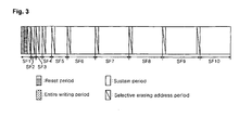
- the entire screen undergoes the entire writing once every frame and unnecessary discharge cells are sequentially turned off every sub-fields SF1 to SF10, as shown in FIG. 3 .
- the first sub-field SF1 includes a reset period, the entire writing period, an erase address period and a sustain period.
- the remaining sub-fields SF2 to SF10 include only the erase address period and the sustain period.
- a sustain pulse as shown in FIG. 4 is applied during the sustain period of the sub-fields SF1 to SF9 so that a stabilized erase address discharge is generated in the remaining sub-fields SF2 to SF10 which do not include the entire writing period.
- a start sustain pulse WISUS is applied to the scan electrode lines Y (or the sustain electrode lines Z). Since the start sustain pulse WISUS has a pulse width wider than that of a normal sustain pulse NSUS, the amount of wall charges within on-cells is larger than the amount obtained when the normal sustain pulse NSUS is applied at the initial stage of the sustain period. The sustain discharge is thus stabilized.
- the normal sustain pulse NSUS is alternately applied to the sustain electrode lines Z and the scan electrode lines Y.
- wall charges are formed in the discharge cell, as shown in FIG. 5a .
- the wall charges of the negative (-) polarity are formed in the scan electrode lines Y and the wall charges of the positive (+) polarity are formed in the sustain electrode lines Z.
- a last sustain pulse WFSUS whose pulse width is set to be wider than that of the normal sustain pulse NSUS is applied to the scan electrode lines Y. Since the pulse width of the last sustain pulse WFSUS is set to be wider, a strong sustain discharge is generated. Accordingly, as shown in FIG. 5b , more wall charges are formed in the discharge cell in comparison to whenever the normal sustain discharge is generated. In other words, more wall charges of the negative (-) polarity are formed on the scan electrode lines Y than when the normal sustain discharge is generated. More wall charges of the positive (+) polarity are formed on the sustain electrode lines Z than when the normal sustain discharge is generated. The wall charges generated by the last sustain pulse WFSUS are employed in an erase discharge of the next address period.
- a small amount of wall charges is formed in the discharge cells by the normal sustain pulse NSUS, as shown in FIG. 5a . Since the last sustain pulse WFSUS is applied with the small amount of the wall charges being formed in the discharge cells, the amount of the wall charges that can be formed by the last sustain pulse WFSUS is limited. Accordingly, sufficient wall charges necessary for an erase discharge of a next address period are not formed. As such, in the conventional selective erasing mode, desired wall charges are not formed during the erase address period. Thus, there is a problem in that an erroneous discharge is generated in the sustain period. More particularly, such an erroneous discharge become more significant when the panel is driven at low temperature ranging from -50°C to 0°C. That is, as movement of particles becomes blunt in a low temperature environment, desired wall charges are not formed by the last sustain pulse WFSUS and the erroneous discharge problem becomes thus more significant.
- the entire cells are turned off during the reset period, and cells to be turned on are selected during the address period. Further, in this mode, during the sustain period, discharging of the on-cells selected by the address discharge is maintained thereby displaying an image.
- the selective writing mode has an advantage in that a range of the gray scale that can be represented is wider than that of the selective erasing mode, but has a disadvantage in that the address period is longer than that of the selective erasing mode.
- the selective erasing mode as shown in FIG. 3 is advantageous in high-speed driving, but is disadvantageous in the limit of the gray scale that can be represented.
- this SWSE mode may have a problem in that desired discharge cells cannot be selected during the erase address period if the panel is driven in the selective erasing mode, especially, at low temperature.
- an object of the present invention is to address at least the problems and disadvantages of the background art.
- An object of the present invention is to provide a method of driving a PDP in which an erroneous discharge is prevented.
- the present invention provides a method of driving a plasma display panel driven in selective erasing mode as set out in claim 1.
- the present invention also provides a method of driving a plasma display panel in which a frame includes selective writing and selective erasing subfields as set out in claim 12.
- a method of driving a PDP driven in a selective erasing mode including the steps of alternately applying a first sustain pulse to scan electrode lines and sustain electrode lines in a sustain period, applying a second sustain pulse having a pulse width wider than that of a first sustain pulse as a last sustain pulse in the sustain period, and before the second sustain pulse is applied, applying a wall charge enhanced pulse to one of the scan electrode lines and the sustain electrode lines.
- a method of driving a plasma display panel in which one frame includes a plurality of selective writing sub-fields and a plurality of selective erasing sub-fields including the steps of alternately applying a first sustain pulse to the scan electrode lines and the sustain electrode lines during a sustain period of one or more selective writing sub-fields and one or more selective erasing sub-fields, applying a second sustain pulse having a pulse width wider than that of a first sustain pulse as a last sustain pulse in the sustain period, and before the second sustain pulse is applied, applying a wall charge enhanced pulse to one of the scan electrode lines and the sustain electrode lines.
- the invention also provides apparatus for driving a plasma display panel adapted to perform the above methods, and a visual display unit comprising a plasma display panel operably driven by such apparatus as set out in claims 23 and 24.
- a method of driving a PDP driven in a selective erasing mode including the steps of alternately applying a first sustain pulse to scan electrode lines and sustain electrode lines in a sustain period, applying a second sustain pulse having a pulse width wider than that of a first sustain pulse as a last sustain pulse in the sustain period, and before the second sustain pulse is applied, applying a wall charge enhanced pulse to one of the scan electrode lines and the sustain electrode lines.
- the method may further include the step of, when the wall charge enhanced pulse is applied, applying a synchronization pulse to the other of the scan electrode lines and the sustain electrode lines to which the wall charge enhanced pulse is not applied so that the synchronization pulse is synchronized with the wall charge enhanced pulse.
- the synchronization pulse may be a square wave.
- the synchronization pulse may be set to have the same voltage value as the first sustain pulse.
- the wall charge enhanced pulse may have a voltage of negative polarity.
- the wall charge enhanced pulse may be a ramp wave that falls with a tilt.
- the wall charge enhanced pulse may fall to a voltage ranging from -80V to -60V.
- the wall charge enhanced pulse may fall to a voltage ranging from -72V to -68V.
- the application time of the wall charge enhanced pulse may be set to be within a range between 2 ⁇ s and 3 ⁇ s.
- the wall charge enhanced pulse may be applied in the sustain period of all the sub-fields included in one frame.
- the wall charge enhanced pulse may be applied in the sustain period of the remaining sub-fields except for the last one among a plurality of sub-fields included in one frame.
- the wall charge enhanced pulse may be applied only when the panel is driven in a low temperature environment.
- FIG. 6 shows a driving waveform supplied in the period of a selective erasing sub-field, for explaining a method of driving a PDP according to a first embodiment.
- a first sub-field of a selective erasing mode includes a reset period, the entire writing period, an erase address period and a sustain period, and the remaining sub-fields of the selective erasing mode include only an erase address period and a sustain period.
- the entire write discharge is generated in the entire discharge cells. While unnecessary discharge cells are sequentially turned off in the remaining sub-fields, an image corresponding to data is displayed.
- pulses of various shapes are applied.
- the ramp pulse RP is applied to the scan electrode lines Y. If the ramp pulse RP is applied to the scan electrode lines Y, a ramp discharge is generated in all of discharge cells and predetermined wall charges are formed by the ramp discharge. In this time, wall charges of the negative (-) polarity are formed in the scan electrode lines Y, and wall charges of the positive (+) polarity are formed in the sustain electrode lines Z.
- the entire writing pulse WP is applied to the sustain electrode lines Z and the scan electrode lines Y.
- the entire writing pulse WP is first applied to the sustain electrode lines Z so that it is overlapped with a voltage value of the wall charges formed in the reset period. As such, if the entire writing pulse WP is applied to the sustain electrode lines Z and the scan electrode lines Y, sufficient wall charges necessary for a sustain discharge are formed in the discharge cells.
- an erase data pulse SED is applied to the address electrode lines X and an erase scan pulse SESCN is also applied to the scan electrode lines Y.
- an erase address discharge is generated in the discharge cells to which the erase data pulse SED and the erase scan pulse SESCN are applied at the same time, whereby the wall charges formed during the entire writing period are erased.
- a start sustain pulse WISUS is applied to the sustain electrode lines Z.
- the start sustain pulse WISUS has a pulse width wider than that of a normal sustain pulse NSUS thereby generating a strong sustain discharge. Accordingly, the amount of wall charges within on-cells, i.e., discharge cells where the erase address discharge is not generated is further increased, thus stabilizing the sustain discharge.
- the normal sustain pulses NSUS is alternately supplied to the sustain electrode lines Z and the scan electrode lines Y.
- This normal sustain pulses NSUS generates the sustain discharge in the on-cells.
- wall charges are formed in the discharge cells, as shown in FIG. 7a .
- wall charges of the negative (-) polarity are formed in the scan electrode lines Y and wall charges of the positive (+) polarity are formed in the sustain electrode lines Z.
- a first wall charge enhanced pulse SR1 is applied to the scan electrode lines Y.
- a second wall charge enhanced pulse SR2 is also applied to the sustain electrode lines Z so that it is synchronized with the first wall charge enhanced pulse SR1.
- the first wall charge enhanced pulse SR1 is applied as a ramp pulse and the second wall charge enhanced pulse SR2 is applied as a square wave. Further, the second wall charge enhanced pulse SR2 may not be applied.
- first wall charge enhanced pulse SR1 and the second wall charge enhanced pulse SR2 are applied, the wall charges formed in the on-cells and the voltage value are added to generate an enhanced discharge.
- first wall charge enhanced pulse SR1 and the second wall charge enhanced pulse SR2 are applied at the same time, a high voltage difference is generated between the scan electrode lines Y and the sustain electrode lines Z, so that a strong enhanced discharge happens.
- first wall charge enhanced pulse SR1 is applied as the ramp pulse, a large amount of the wall charges as shown in FIG. 7b is formed in the on-cells by the enhanced discharge.
- a voltage of the first wall charge enhanced pulse SR1 is set between -80V and -60V, preferably between -72V and -68V so that a large amount of wall charges is sufficiently formed in the on-cells.
- a voltage value of the second wall charge enhanced pulse SR2 is set to be identical to that of the sustain pulses NSUS.
- the application time of the first and second wall charge enhanced pulses SR1, SR2 is set to be within a range between 2 ⁇ s and 3 ⁇ s.
- a last sustain pulse WFSUS having a wide pulse width is applied to the scan electrode lines Y. If the last sustain pulse WFSUS having this wide pulse width is applied, a strong sustain discharge is generated and many wall charges are thus formed. More particularly, the last sustain pulse WFSUS is overlapped with the voltage of the large amount of the wall charges formed by the first and second enhanced pulses SR1, SR2. As a result, sufficient wall charges as shown in FIG. 7c , which are necessary for an erase address period of a next sub-field, can be formed.
- the first wall charge enhanced pulse SR1 and the second wall charge enhanced pulse SR2 can be applied to the sustain period of the entire sub-fields.
- sufficient wall charges can be formed so that the first and second wall charge enhanced pulses SR1, SR2 are applied to the sustain period of all the sub-fields and a stabilized erase discharge is thus generated in an erase address period of a next sub-field.
- the first and second wall charge enhanced pulses SR1, SR2 can be applied to the sustain period of the remaining sub-fields except for the last sub-field. Practically, since a first sub-field of a next frame is located after the last sub-field, the first and second wall charge enhanced pulses SR1, SR2 cannot be applied.
- the first and second wall charge enhanced pulses SR1, SR2 can be applied only when the panel is driven at low temperature, e.g., at a temperature ranging from - 50°C to 0°C.
- the first and second wall charge enhanced pulses SR1, SR2 may not be applied, but only when the panel is driven at low temperature, the first and second wall charge enhanced pulses SR1, SR2 can be applied.
- the panel can be driven at low temperature in a stable manner.
- a method of driving a plasma display panel in which one frame includes a plurality of selective writing sub-fields and a plurality of selective erasing sub-fields including the steps of alternately applying a first sustain pulse to the scan electrode lines and the sustain electrode lines during a sustain period of one or more selective writing sub-fields and one or more selective erasing sub-fields, applying a second sustain pulse having a pulse width wider than that of a first sustain pulse as a last sustain pulse in the sustain period, and before the second sustain pulse is applied, applying a wall charge enhanced pulse to one of the scan electrode lines and the sustain electrode lines.
- the method may further include the step of, when the wall charge enhanced pulse is applied, applying a synchronization pulse to the other of the scan electrode lines and the sustain electrode lines to which the wall charge enhanced pulse is not applied so that the synchronization pulse is synchronized with the wall charge enhanced pulse.
- the synchronization pulse may be a square wave.
- the synchronization pulse may be set to have the same voltage value as the first sustain pulse.
- the wall charge enhanced pulse may have a voltage of negative polarity.
- the wall charge enhanced pulse may be a ramp wave that falls with a tilt.
- the wall charge enhanced pulse may fall to a voltage ranging from -80V to -60V.
- the wall charge enhanced pulse may fall to a voltage ranging from -72V to -68V.
- the application time of the wall charge enhanced pulse may be set to be within a range between 2 ⁇ s and 3 ⁇ s.
- the wall charge enhanced pulse may be applied in the sustain period of the selective erasing sub-fields and the sustain period of the last selective writing sub-field located before the selective erasing sub-field.
- the wall charge enhanced pulse may be applied in the sustain period of the remaining selective erasing sub-fields except for the last selective erasing sub-field and the sustain period of the last selective writing sub-field located before the selective erasing sub-field.
- the wall charge enhanced pulse may be applied only when the panel is driven in a low temperature environment.
- FIG. 8 shows a state where selective erasing sub-fields and selective writing sub-fields are positioned within one frame when the PDP is driven.
- one frame of a SWSE mode includes a selective writing sub-field WSF having one or more subfields, and a selective erasing sub-field ESF having one or more sub-fields.
- the selective writing sub-field WSF includes a m plurality (where, m is a positive integer greater than 0) of sub-fields SF1 to SFm.
- Each of the first to (m-1) th subfields SF1 to SFm-1 except for the m th sub-field SFm is driven with it being divided into a reset period for uniformly forming a given amount of wall charges in cells of the entire screen, a writing address period for selecting on-cells using a write discharge, a sustain period for generating a sustain discharge in the selected on-cells, and an erase period for erasing wall charges within cells after the sustain discharge.
- the m th sub-field SFm being the last sub-field of the selective writing sub-field WSF is divided into a reset period, a writing address period and a sustain period.
- the reset period, the write address period and the erase period of the selective writing sub-field WSF are set to have the same brightness weight every sub-fields SF1 to SFm, but the sustain period thereof is set to have identical or different brightness weight.
- the selective erasing sub-field ESF includes a n-m (wherein, n is a positive integer greater than m) of sub-fields SFm+1 to SFn.
- Each of the (m+1) th to n th sub-fields SFm+1 to SFn is divided into an erase address period for selecting off-cells using an erase discharge and a sustain period for generating a sustain discharge in on-cells.
- the erase address period is set to be identical
- the sustain period is set to be identical or different depending on a relative brightness ratio.
- FIG. 9 shows a driving waveform supplied in the periods of a selective erasing sub-field and a selective writing sub-field, for explaining a method of driving a PDP according to a second embodiment of the present invention.
- a ramp-up pulse RPSU and a ramp-down pulse RPSD are applied to the entire scan electrode lines Y. If the ramp-up pulse RPSU is applied to the scan electrode lines Y, a set-up discharge is generated thereby forming uniform wall charges in the discharge cells. Further, if the ramp-down pulse RPSD is applied to the scan electrode lines Y, a set-down discharge is generated thereby erasing some of wall charges formed redundantly. Meanwhile, when the ramp-down pulse RPSD is applied to the scan electrode lines Y, a DC voltage (Va) of the positive polarity is applied to the sustain electrode lines Z.
- Va DC voltage
- a write data pulse SWD is applied to the address electrode lines X so that it is synchronized with the write scan pulse SWSCN. Then, as a voltage of the write scan pulse SWSCN and the write data pulse SWD and a wall voltage within the cell, which is accumulated previously, are added, a write discharge is generated in the cells to which the write data pulse SWD is applied and on-cells are thus selected. Further, wall charges of the positive polarity are accumulated on the scan electrode line Y and wall charges of negative polarity are accumulated on the sustain electrode line Z and the address electrode line X, by means of the write discharge. The wall charges formed thus serve to lower a voltage applied externally for generating a sustain discharge during the sustain period, i.e., a sustain voltage.
- a start sustain pulse WISUS1 is applied to the scan electrode lines Y.
- the start sustain pulse WISUS1 has a pulse width wider than that of a normal sustain pulse NSUS. Thus, this increases the amount of wall charges within on-cells than those when the normal sustain pulse NSUS is first applied to the sustain period, thereby stabilizing the sustain discharge.
- the normal sustain pulse NSUS is alternately applied to the sustain electrode lines Z and the scan electrode lines Y.
- an erase pulse ERS is supplied in the first to (m-1) th sub-fields SF1 to SFm-1 except for the m th sub-field SFm being a preceding sub-field of the selective erasing sub-field ESF, the on-cells are turned off.
- the last sustain pulse WFSUS of the m th sub-field SFm being the last sub-field of the selective writing sub-field WSF forms wall charges necessary for the period of a subsequent selective erasing sub-field whose pulse width is set to be wider than that of the normal sustain pulse NSUS.
- a first wall charge enhanced pulse SR1 is applied to the scan electrode lines Y
- a second wall charge enhanced pulse SR2 is applied to the sustain electrode lines Z so that it is synchronized with the first wall charge enhanced pulse SR1.
- the first wall charge enhanced pulse SR1 is applied as a ramp pulse and the second wall charge enhanced pulse SR2 is applied as a square wave.
- first wall charge enhanced pulse SR1 and the second wall charge enhanced pulse SR2 are applied, the wall charges formed in the on-cells and the voltage value are added to generate an enhanced discharge.
- first wall charge enhanced pulse SR1 and the second wall charge enhanced pulse SR2 are applied at the same time, a high voltage difference is generated between the scan electrode lines Y and the sustain electrode lines Z, so that a strong enhanced discharge happens.
- first wall charge enhanced pulse SR1 is applied as the ramp pulse, a large amount of the wall charges as shown in FIG. 7b is formed in the on-cells by the enhanced discharge.
- a voltage of the first wall charge enhanced pulse SR1 is set between -80V and -60V, preferably between -72V and -68V so that a large amount of wall charges is sufficiently formed in the on-cells.
- a voltage value of the second wall charge enhanced pulse SR2 is set to be identical to that of the sustain pulses NSUS.
- the application time of the first and second wall charge enhanced pulses SR1, SR2 is set to be within a range between 2 ⁇ s and 3 ⁇ s.
- first and second wall charge enhanced pulses SR1, SR2 are applied before the last sustain pulse WFSUS is applied, a strong sustain discharge is generated by the last sustain pulse WFSUS. Accordingly, sufficient wall charges necessary for an erase address period of a next sub-field can be formed, as shown in FIG. 7c .
- an erase scan pulse SESCN is sequentially applied to the scan electrode lines Y, and an erase data pulse SED which is synchronized with the erase scan pulse SESCN is also applied to the address electrode lines X.
- an erase discharge is generated within the on-cells to which the erase data pulse SED is applied. Accordingly, the wall charges within the on-cells are erased by the erase discharge to the degree that does not generate a discharge although the sustain voltage is applied.
- a start sustain pulse WISUS2 having a wide pulse width is applied to the sustain electrode lines Z so that a sustain discharge can be generated stably.
- the normal sustain pulse NSUS is then alternately applied to the scan electrode lines Y and the sustain electrode lines Z whereby a sustain discharge is generated within the on-cells.
- a last sustain pulse WFSUS is applied to the scan electrode lines Y, thus forming wall charges necessary for a subsequent erase address period.
- the first and second wall charge enhanced pulses SR1, SR2 are applied to the scan electrode lines Y and the sustain electrode lines Z, respectively, so that a plurality of wall charges are formed in the on-cells. Therefore, sufficient wall charges necessary for a next erase address period can be formed by the last sustain pulse WFSUS.
- the first and second wall charge enhanced pulses SR1, SR2 are applied in the sustain period of the last selective writing sub-field SFm and the sustain period of all the selective erasing sub-fields ESF.
- the first and second wall charge enhanced pulses SR1, SR2 may not be applied.
- the first sub-field SF1 of a next frame is located. It is thus not necessary to enhance wall charges by applying the first and second wall charge enhanced pulses SR1, SR2.
- whether the first and second wall charge enhanced pulses SR1, SR2 will be applied in the sustain period of the last selective erasing sub-field SFn can be decided depending on a designer.
- the first and second wall charge enhanced pulses SR1, SR2 can be applied only when a panel is driven at low temperature, for example, ranging from -50°C to 0°C. In other words, when the panel is driven at a temperature higher than the low temperature, the first and second wall charge enhanced pulses SR1, SR2 are not applied. Only when the panel is driven at low temperature, the first and second wall charge enhanced pulses SR1, SR2 can be applied. As such, if the first and second wall charge enhanced pulses SR1, SR2 are applied in a low temperature environment, the panel can be driven stably at low temperature.
- a strong sustain discharge is generated by the last sustain pulse. Therefore, sufficient wall charges necessary for a next erase address period can be formed and an erroneous discharge can be thus prevented.
Applications Claiming Priority (2)
| Application Number | Priority Date | Filing Date | Title |
|---|---|---|---|
| KR2003078850 | 2003-11-08 | ||
| KR10-2003-0078850A KR100524310B1 (ko) | 2003-11-08 | 2003-11-08 | 플라즈마 디스플레이 패널의 구동방법 |
Publications (3)
| Publication Number | Publication Date |
|---|---|
| EP1530193A2 EP1530193A2 (en) | 2005-05-11 |
| EP1530193A3 EP1530193A3 (en) | 2006-06-28 |
| EP1530193B1 true EP1530193B1 (en) | 2012-01-25 |
Family
ID=34431741
Family Applications (1)
| Application Number | Title | Priority Date | Filing Date |
|---|---|---|---|
| EP04256892A Expired - Fee Related EP1530193B1 (en) | 2003-11-08 | 2004-11-08 | Method and apparatus for driving a plasma display panel |
Country Status (6)
| Country | Link |
|---|---|
| US (1) | US20050162351A1 (ja) |
| EP (1) | EP1530193B1 (ja) |
| JP (1) | JP4639070B2 (ja) |
| KR (1) | KR100524310B1 (ja) |
| CN (1) | CN100373433C (ja) |
| TW (1) | TWI259429B (ja) |
Families Citing this family (11)
| Publication number | Priority date | Publication date | Assignee | Title |
|---|---|---|---|---|
| KR100612312B1 (ko) * | 2004-11-05 | 2006-08-16 | 삼성에스디아이 주식회사 | 플라즈마 표시 장치 및 그의 구동 방법 |
| KR100637512B1 (ko) * | 2004-11-09 | 2006-10-23 | 삼성에스디아이 주식회사 | 플라즈마 표시 패널의 구동 방법 및 플라즈마 표시 장치 |
| KR100667538B1 (ko) * | 2005-05-30 | 2007-01-12 | 엘지전자 주식회사 | 플라즈마 디스플레이 장치 및 그의 구동 방법 |
| KR100708691B1 (ko) | 2005-06-11 | 2007-04-17 | 삼성에스디아이 주식회사 | 플라즈마 디스플레이 패널의 구동 방법 및 그 구동 방법에의해 구동되는 플라즈마 디스플레이 패널 |
| EP1912199A4 (en) * | 2005-08-04 | 2009-09-16 | Hitachi Plasma Display Ltd | PLASMA SCREEN DEVICE AND ITS CONTROL METHOD |
| KR100684735B1 (ko) * | 2005-10-12 | 2007-02-20 | 삼성에스디아이 주식회사 | 플라즈마 표시 장치 및 그 구동 방법 |
| KR100728163B1 (ko) * | 2005-10-12 | 2007-06-13 | 삼성에스디아이 주식회사 | 플라즈마 표시 장치 및 그 구동 방법 |
| KR20070118915A (ko) * | 2006-06-13 | 2007-12-18 | 엘지전자 주식회사 | 플라즈마 디스플레이 패널의 구동 방법 |
| KR100811474B1 (ko) * | 2006-10-27 | 2008-03-07 | 엘지전자 주식회사 | 플라즈마 디스플레이 장치 |
| KR100775383B1 (ko) | 2006-11-29 | 2007-11-12 | 엘지전자 주식회사 | 플라즈마 디스플레이 장치 |
| KR20100009952A (ko) * | 2008-07-21 | 2010-01-29 | 삼성에스디아이 주식회사 | 플라즈마 표시 패널의 구동 방법, 및 이 방법을 채용한플라즈마 표시 장치 |
Family Cites Families (10)
| Publication number | Priority date | Publication date | Assignee | Title |
|---|---|---|---|---|
| US4140945A (en) * | 1978-01-06 | 1979-02-20 | Owens-Illinois, Inc. | Sustainer wave form having enhancement pulse for increased brightness in a gas discharge device |
| JPH11327505A (ja) * | 1998-05-20 | 1999-11-26 | Fujitsu Ltd | プラズマディスプレイ装置の駆動方法 |
| JP3578323B2 (ja) * | 1998-12-25 | 2004-10-20 | パイオニア株式会社 | プラズマディスプレイパネルの駆動方法 |
| EP1020838A1 (en) * | 1998-12-25 | 2000-07-19 | Pioneer Corporation | Method for driving a plasma display panel |
| JP3644844B2 (ja) * | 1999-01-11 | 2005-05-11 | パイオニア株式会社 | プラズマディスプレイパネルの駆動方法 |
| JP4357107B2 (ja) * | 2000-10-05 | 2009-11-04 | 日立プラズマディスプレイ株式会社 | プラズマディスプレイの駆動方法 |
| JP4606612B2 (ja) * | 2001-02-05 | 2011-01-05 | 日立プラズマディスプレイ株式会社 | プラズマディスプレイパネルの駆動方法 |
| JP5063841B2 (ja) * | 2001-06-27 | 2012-10-31 | パナソニック株式会社 | プラズマディスプレイパネルの駆動方法 |
| JP4299987B2 (ja) * | 2001-12-21 | 2009-07-22 | 株式会社日立製作所 | プラズマディスプレイ装置及びその駆動方法 |
| KR100525733B1 (ko) * | 2003-05-27 | 2005-11-04 | 엘지전자 주식회사 | 플라즈마 디스플레이 패널의 구동방법 및 장치 |
-
2003
- 2003-11-08 KR KR10-2003-0078850A patent/KR100524310B1/ko not_active IP Right Cessation
-
2004
- 2004-11-08 TW TW093134000A patent/TWI259429B/zh not_active IP Right Cessation
- 2004-11-08 CN CNB2004100883114A patent/CN100373433C/zh not_active Expired - Fee Related
- 2004-11-08 JP JP2004323337A patent/JP4639070B2/ja not_active Expired - Fee Related
- 2004-11-08 EP EP04256892A patent/EP1530193B1/en not_active Expired - Fee Related
- 2004-11-08 US US10/983,094 patent/US20050162351A1/en not_active Abandoned
Also Published As
| Publication number | Publication date |
|---|---|
| TWI259429B (en) | 2006-08-01 |
| JP2005141233A (ja) | 2005-06-02 |
| KR100524310B1 (ko) | 2005-10-28 |
| EP1530193A3 (en) | 2006-06-28 |
| CN1614665A (zh) | 2005-05-11 |
| EP1530193A2 (en) | 2005-05-11 |
| CN100373433C (zh) | 2008-03-05 |
| JP4639070B2 (ja) | 2011-02-23 |
| TW200527353A (en) | 2005-08-16 |
| US20050162351A1 (en) | 2005-07-28 |
| KR20050044949A (ko) | 2005-05-16 |
Similar Documents
| Publication | Publication Date | Title |
|---|---|---|
| US7508359B2 (en) | Method of driving a plasma display panel | |
| US20090128532A1 (en) | Method for driving a plasma display panel | |
| KR100503603B1 (ko) | 플라즈마 디스플레이 패널의 구동방법 | |
| EP1530193B1 (en) | Method and apparatus for driving a plasma display panel | |
| KR100604275B1 (ko) | 플라즈마 디스플레이 패널의 구동방법 | |
| EP1528532B1 (en) | Method and apparatus for driving a plasma display panel | |
| KR100524309B1 (ko) | 플라즈마 디스플레이 패널의 구동방법 | |
| KR100751931B1 (ko) | 플라즈마 디스플레이 패널 및 그 구동방법 | |
| KR100489276B1 (ko) | 플라즈마 디스플레이 패널의 구동방법 | |
| KR100551124B1 (ko) | 플라즈마 디스플레이 패널의 구동 방법 | |
| KR100517472B1 (ko) | 플라즈마 디스플레이 패널의 구동방법 | |
| KR100647776B1 (ko) | 플라즈마 디스플레이 패널의 구동방법 | |
| KR100493614B1 (ko) | 플라즈마 디스플레이 패널의 구동방법 | |
| KR100640053B1 (ko) | 플라즈마 디스플레이 패널의 구동방법 | |
| KR100493617B1 (ko) | 플라즈마 디스플레이 패널의 구동방법 | |
| KR100488456B1 (ko) | 플라즈마 디스플레이 패널의 구동 방법 | |
| KR100480470B1 (ko) | 플라즈마 디스플레이 패널의 구동방법 | |
| KR100533729B1 (ko) | 플라즈마 디스플레이 패널의 구동방법 | |
| KR100511794B1 (ko) | 플라즈마 디스플레이 패널의 구동방법 | |
| KR100493621B1 (ko) | 플라즈마 디스플레이 패널의 구동방법 | |
| KR100801476B1 (ko) | 플라즈마 디스플레이 패널의 구동방법 및 이를 이용한플라즈마 디스플레이 패널 | |
| KR100553931B1 (ko) | 플라즈마 디스플레이 패널의 구동방법 | |
| KR20060079027A (ko) | 플라즈마 디스플레이 패널의 구동방법 |
Legal Events
| Date | Code | Title | Description |
|---|---|---|---|
| PUAI | Public reference made under article 153(3) epc to a published international application that has entered the european phase |
Free format text: ORIGINAL CODE: 0009012 |
|
| AK | Designated contracting states |
Kind code of ref document: A2 Designated state(s): AT BE BG CH CY CZ DE DK EE ES FI FR GB GR HU IE IS IT LI LU MC NL PL PT RO SE SI SK TR |
|
| AX | Request for extension of the european patent |
Extension state: AL HR LT LV MK YU |
|
| PUAL | Search report despatched |
Free format text: ORIGINAL CODE: 0009013 |
|
| AK | Designated contracting states |
Kind code of ref document: A3 Designated state(s): AT BE BG CH CY CZ DE DK EE ES FI FR GB GR HU IE IS IT LI LU MC NL PL PT RO SE SI SK TR |
|
| AX | Request for extension of the european patent |
Extension state: AL HR LT LV MK YU |
|
| 17P | Request for examination filed |
Effective date: 20060623 |
|
| AKX | Designation fees paid |
Designated state(s): DE FR GB NL |
|
| 17Q | First examination report despatched |
Effective date: 20071102 |
|
| GRAP | Despatch of communication of intention to grant a patent |
Free format text: ORIGINAL CODE: EPIDOSNIGR1 |
|
| RIN1 | Information on inventor provided before grant (corrected) |
Inventor name: KIM, SO NIC |
|
| GRAS | Grant fee paid |
Free format text: ORIGINAL CODE: EPIDOSNIGR3 |
|
| GRAA | (expected) grant |
Free format text: ORIGINAL CODE: 0009210 |
|
| AK | Designated contracting states |
Kind code of ref document: B1 Designated state(s): DE FR GB NL |
|
| REG | Reference to a national code |
Ref country code: GB Ref legal event code: FG4D |
|
| REG | Reference to a national code |
Ref country code: NL Ref legal event code: T3 |
|
| REG | Reference to a national code |
Ref country code: DE Ref legal event code: R096 Ref document number: 602004036258 Country of ref document: DE Effective date: 20120322 |
|
| PLBE | No opposition filed within time limit |
Free format text: ORIGINAL CODE: 0009261 |
|
| STAA | Information on the status of an ep patent application or granted ep patent |
Free format text: STATUS: NO OPPOSITION FILED WITHIN TIME LIMIT |
|
| 26N | No opposition filed |
Effective date: 20121026 |
|
| REG | Reference to a national code |
Ref country code: DE Ref legal event code: R097 Ref document number: 602004036258 Country of ref document: DE Effective date: 20121026 |
|
| PGFP | Annual fee paid to national office [announced via postgrant information from national office to epo] |
Ref country code: NL Payment date: 20121015 Year of fee payment: 9 |
|
| GBPC | Gb: european patent ceased through non-payment of renewal fee |
Effective date: 20121108 |
|
| REG | Reference to a national code |
Ref country code: FR Ref legal event code: ST Effective date: 20130731 |
|
| PG25 | Lapsed in a contracting state [announced via postgrant information from national office to epo] |
Ref country code: GB Free format text: LAPSE BECAUSE OF NON-PAYMENT OF DUE FEES Effective date: 20121108 Ref country code: FR Free format text: LAPSE BECAUSE OF NON-PAYMENT OF DUE FEES Effective date: 20121130 |
|
| PGFP | Annual fee paid to national office [announced via postgrant information from national office to epo] |
Ref country code: DE Payment date: 20131015 Year of fee payment: 10 |
|
| REG | Reference to a national code |
Ref country code: NL Ref legal event code: V1 Effective date: 20140601 |
|
| PG25 | Lapsed in a contracting state [announced via postgrant information from national office to epo] |
Ref country code: NL Free format text: LAPSE BECAUSE OF NON-PAYMENT OF DUE FEES Effective date: 20140601 |
|
| REG | Reference to a national code |
Ref country code: DE Ref legal event code: R119 Ref document number: 602004036258 Country of ref document: DE |
|
| PG25 | Lapsed in a contracting state [announced via postgrant information from national office to epo] |
Ref country code: DE Free format text: LAPSE BECAUSE OF NON-PAYMENT OF DUE FEES Effective date: 20150602 |