EP1526401A1 - Module de dispositif optique à réglage thermique - Google Patents
Module de dispositif optique à réglage thermique Download PDFInfo
- Publication number
- EP1526401A1 EP1526401A1 EP04007641A EP04007641A EP1526401A1 EP 1526401 A1 EP1526401 A1 EP 1526401A1 EP 04007641 A EP04007641 A EP 04007641A EP 04007641 A EP04007641 A EP 04007641A EP 1526401 A1 EP1526401 A1 EP 1526401A1
- Authority
- EP
- European Patent Office
- Prior art keywords
- heat
- optical device
- insulating
- device module
- module according
- Prior art date
- Legal status (The legal status is an assumption and is not a legal conclusion. Google has not performed a legal analysis and makes no representation as to the accuracy of the status listed.)
- Granted
Links
Images


Classifications
-
- G—PHYSICS
- G02—OPTICS
- G02B—OPTICAL ELEMENTS, SYSTEMS OR APPARATUS
- G02B7/00—Mountings, adjusting means, or light-tight connections, for optical elements
- G02B7/008—Mountings, adjusting means, or light-tight connections, for optical elements with means for compensating for changes in temperature or for controlling the temperature; thermal stabilisation
-
- G—PHYSICS
- G02—OPTICS
- G02F—OPTICAL DEVICES OR ARRANGEMENTS FOR THE CONTROL OF LIGHT BY MODIFICATION OF THE OPTICAL PROPERTIES OF THE MEDIA OF THE ELEMENTS INVOLVED THEREIN; NON-LINEAR OPTICS; FREQUENCY-CHANGING OF LIGHT; OPTICAL LOGIC ELEMENTS; OPTICAL ANALOGUE/DIGITAL CONVERTERS
- G02F1/00—Devices or arrangements for the control of the intensity, colour, phase, polarisation or direction of light arriving from an independent light source, e.g. switching, gating or modulating; Non-linear optics
- G02F1/01—Devices or arrangements for the control of the intensity, colour, phase, polarisation or direction of light arriving from an independent light source, e.g. switching, gating or modulating; Non-linear optics for the control of the intensity, phase, polarisation or colour
- G02F1/11—Devices or arrangements for the control of the intensity, colour, phase, polarisation or direction of light arriving from an independent light source, e.g. switching, gating or modulating; Non-linear optics for the control of the intensity, phase, polarisation or colour based on acousto-optical elements, e.g. using variable diffraction by sound or like mechanical waves
- G02F1/116—Devices or arrangements for the control of the intensity, colour, phase, polarisation or direction of light arriving from an independent light source, e.g. switching, gating or modulating; Non-linear optics for the control of the intensity, phase, polarisation or colour based on acousto-optical elements, e.g. using variable diffraction by sound or like mechanical waves using an optically anisotropic medium, wherein the incident and the diffracted light waves have different polarizations, e.g. acousto-optic tunable filter [AOTF]
-
- G—PHYSICS
- G02—OPTICS
- G02F—OPTICAL DEVICES OR ARRANGEMENTS FOR THE CONTROL OF LIGHT BY MODIFICATION OF THE OPTICAL PROPERTIES OF THE MEDIA OF THE ELEMENTS INVOLVED THEREIN; NON-LINEAR OPTICS; FREQUENCY-CHANGING OF LIGHT; OPTICAL LOGIC ELEMENTS; OPTICAL ANALOGUE/DIGITAL CONVERTERS
- G02F2203/00—Function characteristic
- G02F2203/60—Temperature independent
Definitions
- the present invention relates to an optical device module that homogenizes temperature distribution in optical devices, such as acousto-optic effect selection filters and arrayed waveguide grating filters, which are used in communication systems that employ wavelength-division multiplexing.
- wavelength-division multiplexing WDM
- WDM wavelength-division multiplexing
- functions of adding and dropping optional wavelengths of light are essential.
- LiNbO3 waveguide type acousto-optic tunable filters AOTF
- the advantage of the AOTF is that multiple wavelengths can be selected simultaneously or wide wavelength band exceeding 100 nanometer (nm) can be selected (see Optorics (1999) No. 5, P155 and The Institute of Electronics, Information and Communication Engineers, OPE 96-123, P79).
- an optical waveguide grating which uses an optical add/drop module array, is also included in main devices under examination.
- the advantage of the optical add/drop module array is that signal wavelength grids having intervals of 0.8 nm to 0.2 nm can be supported in the device.
- the AOTF 202 of LiNbO3 waveguide type according to (1) generally has heater 234 positioned with soaking plate 232, for example, copper plate, etc. intervened on the rear surface of x-cut LiNbO3 substrate 204 as shown in Fig. 29, and modularized in package (PKG) 236 together with this heater 234.
- the heat conductivity in module construction of AOTF 202 can be assumed to be obtained by connecting heat resistance Rln of LiNbO3 substrate 204 as well as ambient (air) heat resistance Rair and heat resistance Rpkg of package 236 in parallel across current source I and external heat source (PKG incoming radiation) Ta as per thermal substrate 204 shown in Fig. 30 when package 236 is formed by material having comparatively high thermal conductivity.
- the temperature distribution of LiNbO3 waveguide type AOTF 202 is investigated.
- the thermal conductivity is high, that is, Rpkg is small, soaking can take place, but (3) indicates that consumption power I of heater 234 increases as Rpkg decreases. That is, even if soaking is carried out, the consumption power of heater 234 increases and it becomes unserviceable.
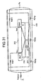
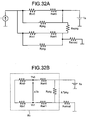
- package 236 is formed by material with low thermal conductivity (see Fig. 31), as is the case of the thermal equivalent circuit shown in Fig. 32A, across current source I and external heat source (PKG incoming radiation) Ta, heat resistance Rln0 of LiNbO3 substrate 204, and ambient heat resistance Rair0 are connected in parallel with heat resistance Rpkg of package 236. Heat resistance Rln1 of LiNbO3 substrate 204 and ambient heat resistance Rair1 in parallel with heat resistance Rpkg of package 236 are further connected in parallel after connecting center heat resistance Rspkg of package 236 across both parallel connections. At the same time, ambient heat resistance Rairout outside package 236 in communication with the ground is connected across heat resistance Rpkg of package 236 and ambient heat resistance Rair1.
- This thermal equivalent circuit can be simplified to a circuit as shown in Fig. 32B in which heat resistance Rln0, heat resistance Rair0 of ambient in PKG, heat resistance Rpkg of LiNbO3 substrate 204, and heat resistance Rair1 of ambient in PKG are connected to center heat resistance Rspkg of package 236 in parallel across external heat source (PKG incoming radiation) Ta and heat resistance Rairout of ambient outside package 236.
- ⁇ Tpkg Ta ⁇ Rc/(Rc+Rairout)
- ⁇ Ts ⁇ Tpkg ⁇ Rln/(Rln+Rair)
- ⁇ Ts (Rc/(Rc+Rairout)) ⁇ (Rln/(Rln+Rair)) ⁇ Ta
- ⁇ Ts Ta ⁇ (Rpkg/Rairout) ⁇ (Rln/Rair)/((Rpkg/Rair+Rln/Rair+1) +(1+Rln/Rair) ⁇ Rpkg/Rairout)
- LiNbO3 waveguide type AOTF 202 Based on the above thermal conductivity, the temperature distribution of LiNbO3 waveguide type AOTF 202 is investigated. In general, since Rln is not extremely smaller than Rair, Rpkg must be extremely smaller than air resistance Rairout, but this is not practical. Consequently, if package 236 is made of material with low thermal conductivity, and the external wall of package 236 is exposed to non-homogeneous outdoor temperature due to heat from an external heat source, the package is susceptible to non-uniformity of the outdoor temperature. Therefore, device (LiNbO3 substrate 204) surface temperature is likely to be non-uniform (temperature gradient is generated).
- the conventional example according to (3) intends to adjust the filter wavelength characteristics by changing the shape and arrangement of a strain providing section after manufacturing an element with the strain providing section for correcting local double refraction index of an optical waveguide.
- it requires extra cost and impairs simplicity from the viewpoint of manufacture.
- it is extremely difficult to correct the difference in refraction index appropriately, in order to obtain completely satisfactory filter characteristics.
- the conventional examples described in (5) and (6) describe a soaking structure in a waveguide device.
- a soaking plate made of a metal with excellent thermal conductivity is inserted between AWG waveguide device and temperature control device (heater, Peltier device).
- temperature control device hereinter, Peltier device.
- the desired temperature uniformity cannot be achieved by this kind of soaking plate alone. That is, with such construction, a heat soaking plate is placed only on the Peltier device and though the temperature is made homogeneous, outside effects are not considered.
- the heat soaking plate that provides good thermal conductivity is provided, consumption power increases.
- the device area in AOTF devices is large. Therefore, problems such as temperature gradient of the heater and temperature gradient caused by difference in heat resistance on the device surface, etc. occur. Therefore, in AOTF devices, the use of the heat soaking plate alone cannot achieve the temperature uniformity in the device. On the other hand, in AWG devices, because the device area increases with the number of channels, temperature uniformity cannot be achieved in the device.
- An optical device module includes an optical device; a soaking unit fixed to one surface of the optical device; a heating/cooling unit fixed to one surface of the soaking unit, wherein the heating/cooling unit performs a function selected from a group consisting of heating the optical device using self-generated heat and cooling the optical device by absorbing heat; a heat-insulating unit fixed to one surface of the heating/cooling unit; and a package that houses the optical device, the soaking unit, the heating/cooling unit, and the heat-insulating unit.
- the heat-insulating unit is fixed to one surface of the package.
- LiNbO3 waveguide type AOTF 202 which is a waveguide type optical device shown in Fig. 27, is applied is described as an example of the optical device. Thereafter, the detailed description of the AOTF 202 is omitted.
- Fig. 1 is a side view of an optical device module according to a first embodiment of the present invention.
- a flat-plate form soaking plate (soaking member) 12 of uniform thickness made of material having good heat conductivity such as copper is joined to the bottom surface of AOTF 202 using an adhesive such as epoxy resin.
- a heat-insulator (heat-insulating means: heat-insulating element) 16 is made of polyphenylene sulfide (PPS), Duracon, or phenol resin, among others and is joined to the bottom surface of heater 14 using an adhesive such as epoxy resin.
- PPS polyphenylene sulfide
- Duracon Duracon
- phenol resin phenol resin
- a top profile of the heat-insulator 16 coincides with the bottom profile of soaking plate 12.
- the bottom surface of heat-insulator 16 is joined to the inner bottom surface of a package (PKG) 18 using adhesive such as epoxy resin.
- adhesive such as epoxy resin.
- the table below shows thermal conductivity of these components. Name Heat conductivity (W/m-°C) PPS 0.26 Duracon 0.30 Phenol resin 0.21
- heat insulator 16 By joining the bottom surface of heat insulator 16 to the inside of package 18, a successively laminating configuration to integrate AOTF 202, soaking plate 12, heater 14, and heat insulator 16, is housed in package 18.
- the package 18 is made of material having good heat conductivity and is formed into an airtight cube (hollow cubic form) shut with lid 20.
- a Peltier element may be used, and in such case, the top surface of the Peltier element is used for heating and the bottom surface for absorbing heat.
- the area of the top surface and the bottom surface of soaking plate 12, heater 14, and heat insulator 16 are smaller than the area of the bottom surface of AOTF 202, but these may be assumed to be identical.
- the soaking plate 12 and AOTF 202 are heated.
- the heat insulator 16 prevents transmission of the heat downwards and almost all of the heat is transmitted upwards to soaking plate 12, thereby efficiently and uniformly heating the soaking plate 12.
- Fig. 2 illustrates results of computer simulation of temperature distribution in an optical device by the optical device module. An overall temperature distribution of 0.3°C or lower is obtained.
- FIG. 3 is a side view of an optical device module according to a second embodiment.
- the configuration of the heat-insulating means is explained in detail.
- the other components of the optical device module are identical to those in the first embodiment, and the detailed description thereof is omitted.
- Fig. 4 is a view of the optical device module as seen from the bottom surface.
- the heat insulating means includes a plurality of heat-insulating elements in the form of square bars that are made of polyphenylene sulfide, Duracon, or phenol resin.
- the heat-insulating elements have varying heat-insulation ratio (thermal conductivity) and are spaced at predetermined intervals, perpendicular to the direction of propagation of incoming lights ⁇ 1 through ⁇ n.
- One surface of the heat-insulating elements is attached to the bottom surface of heater 14 and the other surface to the inner bottom surface of package 18.
- the length of each of the square-bars of the heat insulator 22 is slightly longer than the breadth of the AOTF 202.
- Fig. 5 is a side view of the optical device module, explaining how heating temperature is transmitted.
- the portion of the soaking plate 12 corresponding to the portion where heat insulator 22 exists reaches a temperature level "a".
- the portion of the soaking plate 12 corresponding to the portion of spatial region 24 reaches the temperature of level "b", which is higher than level "a”.
- On the surface of AOTF 202 a plurality of arc-shaped regions of temperature level "c" is formed, each centered around the temperature level b.
- the entire surface of the AOTF 202 is assumed to reach a uniform temperature level "d". In other words, the same results as shown in Fig. 2 can be obtained.
- spatial regions 24 of air insulation are interleaved between heat insulators 22. Therefore, the heating temperature of the whole of heater 14 can be transmitted efficiently to soaking plate 12, thereby saving energy and at the same time, reducing the volume of the material used for the heat insulators. Consequently, keeping the surface temperature of the AOTF 202 uniform further reduces cost. Moreover, the AOTF 202 exhibits satisfactory filter characteristics, and it becomes easy to promote multi-channeling and increase the functionality.
- FIG. 6 is a side view of essential portion of the optical device module according to the third embodiment, together with temperature characteristics.
- Fig. 7 is a side view of the essential portion, and another example of temperature characteristics.
- the configuration of the heat insulating means is explained in detail.
- the other components of the optical device module are identical to those in the first and second embodiments, and the detailed description thereof is omitted.
- the heat insulating means is formed by a plurality of square bars (heat insulating elements) 42 identical in shape, made of polyphenylene sulfide, Duracon, or phenol resin, etc., and attached to the bottom surface of heater 14.
- a plurality of spatial regions 44 providing air heat insulation are formed between the square bars.
- the heat insulators 42 are placed in a direction perpendicular to the direction of propagation of the incoming light.
- the space between the plurality of heat insulators 42 is not identical, the spatial regions 44 are coarse or densely spaced.
- each of the heat insulators 42 is joined to the inner bottom surface of package 18 by adhesive such as epoxy resin, etc.
- the temperature of the center of heater 14 is likely to be lower than that of the other regions, as seen from temperature characteristics of heat-generating resistors in heater 14 (concave temperature distribution due to non-uniformity of the heater: see pattern A in Fig. 6).
- the region where the intervals between the heat insulators 42 are coarse corresponds to the center region of heater 14, and the region where the intervals between the heat insulators 42 are dense corresponds to the regions on both ends of the heater 14.
- the temperature of the coarse regions is comparatively high (convex temperature distribution due to heat insulator: see pattern B in Fig. 6) and mutually compensates for the concave temperature distribution of heater 14, thereby homogenizing the temperature distribution of the AOTF 202 (see pattern C in Fig. 6).
- the temperature of the center of heater 14 is likely to be higher than that of the other regions, as seen from temperature characteristics of heat-generating resistors in heater 14 (convex temperature distribution due to non-uniformity of the heater: see pattern A in Fig. 7).
- the region where the intervals between the heat insulators 42 are coarse corresponds to the region on both ends of heater 14, and the region where the intervals between the heat insulators 42 are dense corresponds to the center region of heater 14.
- the total heat insulation provided by the coarse region of heat insulator 42 is large. Therefore, the temperature of the coarse region is comparatively high (concave temperature distribution due to heat insulator: see pattern B in Fig. 7) and mutually compensates for the convex temperature distribution of heater 14, thereby homogenizing the temperature distribution of the AOTF 202 (see pattern C in Fig. 7).
- the coarse and dense regions between the heat insulators 42 are configured based on the temperature distribution characteristics of the heater 14. Therefore, the temperature distribution of the soaking plate 12 can be homogenized appropriately, and the entire region of AOTF 202 can be uniformly heated. Moreover, merely by adjusting the intervals between the heat insulators 42 to be either coarse or dense, it is possible to keep the surface temperature of AOTF uniform. Consequently, cost is reduced, satisfactory filter characteristics of AOTF are exhibited and maintained, and at the same time, multi-channeling can be promoted and functionality increases. Furthermore, because the heat insulators 42 have spatial regions 44 for communication with the inside of package 18, air inside each spatial region 44 can be evacuated. ,Consequently, air inside each of the spatial regions 44 does not expand and excellent heat insulating effects are achieved.
- FIG. 8 illustrates an essential portion viewed from the bottom surface of the optical device module according to a fourth embodiment.
- the configuration of the heat-insulating means is explained in detail.
- the other components of the optical device module are identical to those in the first embodiment, and the detailed description thereof is omitted.
- the heat insulating means includes heat-insulating elements 52 with identical cross sections and made of polyphenylene sulfide, Duracon, or phenol resin, etc.
- the heat-insulating elements 52 are meandrous and form spatial regions 54 for air heat insulation.
- the spatial regions 54 are spaced at predetermined intervals perpendicular to the direction of propagation of incoming light.
- the heat insulators 52 cut across the bottom surface of heater 14 are connected on alternate ends, and are integrated into one piece.
- the meandering heat insulators 52 are joined to the bottom surface of heater 14 and to the inner bottom surface of package 18 (see Fig. 1) by adhesive such as epoxy resin.
- the use of meandering heat insulators 52 simplifies production and positioning of the heater 14 and heat insulators 52. Consequently, fabrication is simplified. Moreover, the temperature distribution of soaking plate 12 can be homogenized appropriately, and the entire region of the AOTF 202 can be uniformly heated. Furthermore, satisfactory filter characteristics of AOTF are exhibited and maintained, and at the same time, multi-channeling can be promoted and functionality increases. Because heat insulators 52 have spatial regions 54 to communicate with the inside of package 18, air inside each spatial region 54 can be evacuated. Consequently, the air inside each of spatial regions 54 does not expand and excellent heat insulating effects are achieved.
- the intervals between meandering heat insulators 52, that is the spatial regions 54 for air heat insulation may be configured to have coarse regions and dense regions based on the heating characteristics of heater 14.
- FIG. 9 illustrates an essential portion viewed from the bottom surface of the optical device module according to the fifth embodiment.
- the configuration of the heat insulating means is explained in detail.
- the other components of the optical device module are identical to those in the first embodiment, and the detailed description thereof is omitted.
- the heat insulating means includes a plurality of heat-insulating elements 62 with identical cross sections and made of polyphenylene sulfide, Duracon, or phenol resin, etc.
- the heat-insulating elements 62 are provided in a form of comb teeth while forming spatial regions 64 for air heat insulation.
- the spatial regions 64 are spaced at predetermined intervals perpendicular to the direction of propagation of incoming light. Consequently, the heat insulators 62 cut across the bottom surface of heater 14, are connected to heat insulator 66 on one end, and are integrated into one piece.
- the comb-teeth shaped heat insulators 62 are joined to the bottom surface of heater 14 and to the inner bottom surface of package 18 (see Fig. 1) by adhesive such as epoxy resin.
- the use of comb-teeth shaped heat insulators 62 simplifies production and positioning of the heater 14 and heat insulators 62. Consequently, fabrication is simplified. Moreover, the temperature distribution of soaking plate 12 can be homogenized appropriately, and the entire region of the AOTF 202 can be heated uniformly. Furthermore, satisfactory filter characteristics of AOTF are exhibited and maintained, and at the same time, multi-channeling can be promoted and functionality increases. Because comb-teeth shaped heat insulators 62 have spatial regions 64 to communicate with the inside of package 18, air inside the spatial region 64 can be evacuated, and consequently, air inside each of spatial regions 64 does not expand and excellent heat insulating effects are achieved.
- the intervals between comb-teeth shaped heat insulators 62, that is the spatial regions 64 for air heat insulation may be configured to have coarse regions and dense regions based on the heating characteristics of heater 14.
- FIG. 10 illustrates an essential portion viewed from the bottom surface of the optical device module according to the sixth embodiment.
- the configuration of the heat insulating means is explained in detail.
- the other components of the optical device module are identical to those in the first embodiment, and the detailed description thereof is omitted.
- the heat insulating means is formed by one pair of heat insulators, each including a plurality of heat-insulating elements.72, 74 with identical cross sections and made of polyphenylene sulfide, Duracon, or phenol resin, etc.
- the heat-insulating elements 72, 74 are provided in a form of comb teeth while forming spatial regions 76, 78 for air heat insulation.
- the spatial regions 76, 78 are spaced at predetermined intervals perpendicular to the direction of propagation of incoming light.
- the comb-teeth shaped insulators 72 are interleaved with the comb-teeth-form insulators 74 so that the plurality of elements of one insulator is placed in the spatial regions of the other insulator.
- the two comb-teeth-form insulators 72, 74 are joined to the bottom surface of heater 14 and to the inner bottom surface of package 18 (see Fig. 1) by adhesive such as epoxy resin, etc.
- the use of comb-teeth shaped heat insulators 72, 74 simplifies production and positioning of the heater 14 and the two comb-teeth shaped heat insulators 72, 74. Consequently, fabrication is simplified. Moreover, the temperature distribution of soaking plate 12 can be homogenized appropriately, and the entire region of the AOTF 202 can be heated uniformly. Furthermore, satisfactory filter characteristics of AOTF are exhibited and maintained, and at the same time, multi-channeling can be promoted and functionality increases. Furthermore, because comb-teeth shaped heat insulators 72, 74 have spatial regions 76, 78 for communication with the inside of package 18, air inside the spatial regions 76, 78 can be evacuated. Consequently, the air inside each of spatial regions 76, 78 does not expand and excellent heat insulating effects are achieved.
- the intervals between comb-teeth shaped heat insulators72, 74, that is, the spatial regions 76, 78 for air heat insulation may be configured to have coarse regions and dense regions based on the heating characteristics of heater 14.
- FIG. 11 illustrates an essential portion viewed from the bottom surface of the optical device module according to the seventh embodiment.
- the configuration of the heat insulating means is explained in detail.
- the other components of the optical device module are identical to those in the first embodiment, and the detailed description thereof is omitted.
- the heat insulating means is formed by a plurality of plate-form heat-insulating elements 84, is made of polyphenylene sulfide, Duracon, or phenol resin, etc. and placed perpendicular to the direction of propagation of incoming light.
- a plurality of spatial regions 82 may be formed by injection and hollowing, (the forming method is optional) for air insulation.
- the spatial regions 82 are spaced at predetermined intervals perpendicular to the direction of propagation of incoming light.
- An air vent 86 that enables ventilation of each of spatial regions 82 is formed on one end of each heat insulating plate.
- Each of these heat insulators 84 is joined to the bottom surface of heater 14 and to the inner bottom surface of package 18 (see Fig. 1) by adhesive such as epoxy resin, etc.
- heat-insulator plate 84 simplifies production and positioning of the heater 14 and heat insulators 84. Consequently, fabrication is simplified. Moreover, the temperature distribution of soaking plate 12 can be homogenized appropriately, and the entire region of the AOTF 202 can be heated uniformly. Furthermore, satisfactory filter characteristics of AOTF are exhibited and maintained, and at the same time, multi-channeling can be promoted and functionality increases. Furthermore, because heat insulator 84 has air vent 86 at one end of each of spatial regions 82 for communication with the inside of package 18, air inside each of spatial regions 82 can be evacuated. Consequently, air inside spatial regions 82 does not expand and excellent heat insulating effects are achieved.
- the intervals between the spatial regions 82 may be configured to have coarse regions and dense regions based on the heating characteristics of heater 14.
- FIG. 12 is a side view an essential portion of the optical device module of the eighth embodiment together with temperature characteristics.
- Fig. 13 and Fig. 14 are views as seen from the bottom surface. The configuration of the heat insulating means is explained in detail. The other components of the optical device module are identical to those in the first embodiment, and the detailed description thereof is omitted.
- the heat insulating means made of polyphenylene sulfide, Duracon, or phenol resin, etc., is in the form of letter X and is a flat-plate heat insulating element 94 having recessed sections 92, 92 for air heat insulation (heat insulating element). Both ends are depressed in the concave shape in order to deal with the case in which the center of heater 14 tends to acquire comparatively high temperature due to patterns of heat-generating resistors inside heater 14 (convex temperature distribution due to non-uniformity of the heater: see pattern A in Fig. 12).
- the X-shaped heat insulator 94 is joined to the bottom surface of heater 14 and to the inner bottom surface of package 18 by adhesive such as epoxy resin, etc.
- the use of previously prepared X-shaped flat-plate heat-insulator 94 simplifies production and positioning of the heater 14 and heat insulators 94. Consequently, fabrication is simplified. Moreover, the X-shaped heat insulator 94 can adapt to the characteristics of heater 14 and homogenize the temperature distribution of soaking plate 12, thereby making it possible to heat the entire area of AOTF 202 to a uniform temperature. Consequently, satisfactory filter characteristics of AOTF 202 are exhibited and maintained, and at the same time, multi-channeling can be promoted and functionality increases. Furthermore, because heat insulator 94 has the spatial regions surrounded by recessed sections 92 for communication with the inside of package 18, air inside the spatial regions surrounded by recessed section 92 can be evacuated. Consequently, air inside the spatial regions surrounded by recessed section 92 does not expand and excellent heat insulating effects are achieved.
- Fig. 15 illustrates results of computer simulation of temperature distribution in an optical device by the optical device module according to the eighth embodiment.
- the use of X-shaped heat insulator 94 achieves temperature uniformity within 0.1°C throughout the full width.
- FIG. 16 illustrates an essential portion of the optical device module of the ninth embodiment together with temperature characteristics.
- Fig. 16 is a side view
- Fig. 17 is a view as seen from the bottom surface.
- the configuration of the heat insulating means is explained in detail.
- the other components of the optical device module are identical to those in the first embodiment, and the detailed description thereof is omitted.
- the heat insulating means is made of polyphenylene sulfide, Duracon, or phenol resin, etc., and is in the form of a flat-plate heat insulating element 104.
- An opening formed at the center serves as the spatial region 102 for air heat insulation.
- the spatial region 102 is shaped in order to deal with the case in which the center of heater 14 tends to acquire comparatively low temperature due to patterns of heat-generating resistors inside heater 14 (concave temperature distribution due to non-uniformity of the heater: see pattern A in Fig. 16).
- Part of spatial region 102 is spatially connected to air vent 106 formed in part of flat-plate heat insulator 104.
- the flat-plate heat insulator 104 is joined to the bottom surface of heater 14 and to the inner bottom surface of package 18 by adhesive such as epoxy resin, etc.
- heat-insulator 104 having spatial region 102 in the center simplifies production and positioning of the heater 14 and heat insulators 104. Consequently, fabrication is simplified. Moreover, the heat insulator 104 that has spatial region 102 in the center can adapt to the characteristics of heater 14 and homogenize the temperature distribution of soaking plate 12, thereby making it possible to heat the entire area of AOTF 202 to a uniform temperature. Consequently, satisfactory filter characteristics of AOTF 202 are exhibited and maintained, and at the same time, multi-channeling can be promoted and functionality increases. Furthermore, because heat insulator 104 has an air vent 106 included in the spatial regions 102 for communication with the inside of package 18, air inside spatial regions 102 can be evacuated. Consequently, air inside each of spatial regions 102 does not expand and excellent heat insulating effects are achieved.
- an additional air vent 106 may be formed at a position opposite to air vent 106, and the number of air vents formed may be set optionally.
- FIG. 18 illustrates an essential portion of the optical device module of the tenth embodiment together with temperature characteristics.
- Fig. 18 is a side view
- Fig. 19 is a view as seen from the bottom surface.
- the configuration of the heat insulating means is explained in detail.
- the other components of the optical device module are identical to those in the first embodiment, and the detailed description thereof is omitted.
- the heat insulating means is made of polyphenylene sulfide, Duracon, or phenol resin, etc., and is in the form of a flat-plate heat insulator (heat insulating element) 118.
- An opening formed at the center serves as the spatial region 112 for air heat insulation (heat-insulating element).
- Recessed spatial regions 114, 116 for air heat insulation (heat insulating element) in the form of concave shape are provided on the forward edge side and backward edge side to deal with the case in which the center of heater 14 tends to acquire comparatively high temperature due to patterns of heat-generating resistors inside heater 14 (convex temperature distribution due to non-uniformity of the heater: see pattern A in Fig. 18).
- Part of spatial region 112 in the center opening is spatially connected to air vent 119 formed in part of flat-plate heat insulator 118.
- the flat-plate heat insulator 118 is joined to the bottom surface of heater 14 and to the inner bottom surface of package 18 by adhesive such as epoxy resin, etc.
- a flat-plate heat-insulator 118 having spatial regions 112, 114, 116 on the center side and on both edges simplifies production and positioning of the heater 14 and heat insulators 118. Consequently, fabrication is simplified.
- the heat insulator 118 that has spatial regions 112, 114, 116 on the center side and on both edges can adapt to the characteristics of heater 14 and homogenize the temperature distribution of soaking plate 12, thereby making it possible to heat the entire area of AOTF 202 to a uniform temperature. Consequently, satisfactory filter characteristics of AOTF 202 are exhibited and maintained, and at the same time, multi-channeling can be promoted and functionality increases.
- heat insulator 118 has an air vent 119 included in the spatial region 112 for communication with the inside of package 18 while other spatial regions 114, 116 directly communicate with the inside of package 18, air inside spatial regions 112, 114, 116 can be evacuated. Consequently, air inside spatial regions 112, 114, 116 does not expand and excellent heat insulating effects are achieved.
- an additional air vent 119 may be formed at a position opposite to air vent 119, and the number of air vents formed may be set optionally.
- FIG. 20 illustrates an essential portion of the optical device module of the eleventh embodiment, together with temperature characteristics.
- Fig. 20 is a side view
- Fig. 21 is a view as seen from the bottom surface.
- the configuration of the heat insulating means is explained in detail.
- the other components of the optical device module are identical to those in the first embodiment, and the detailed description thereof is omitted.
- the heat insulating means is made of polyphenylene sulfide, Duracon, or phenol resin, etc., and is configured as flat-plate heat insulator (heat insulating element) 128. Openings formed on two sides of the center of the heat insulator 128, serve as the spatial regions 122, 124 for air heat insulation (heat-insulating element). An air vent 126 spatially connected to both spatial regions 122, 124 on one end are provided to deal with the case in which the center side of heater 14 tends to acquire comparatively low temperature on both sides of the center of heater 14 due to patterns of heat-generating resistors inside heater 14 (concave temperature distribution due to non-uniformity of the heater: see pattern A in Fig. 20).
- the flat-plate heat insulator 128 is joined to the bottom surface of heater 14 and to the inner bottom surface of package 18 by adhesive such as epoxy resin, etc.
- flat-plate heat-insulator 128 that has spatial regions 122, 124, on both sides of the center simplifies production and positioning of the heater 14 and heat insulators 128. Consequently, fabrication is simplified. Moreover, the heat insulator 128 that has spatial regions 122, 124 on both sides of the center can adapt to the characteristics of heater 14 and homogenize the temperature distribution of soaking plate 12, thereby making it possible to heat the entire area of AOTF 202 to a uniform temperature. Consequently, satisfactory filter characteristics of AOTF 202 are exhibited and maintained, and at the same time, multi-channeling can be promoted and functionality increases.
- spatial regions 122, 124 of heat insulator 128 communicate with the inside of package 18 via air vent 126, air inside spatial regions 122, 124 can be evacuated. Consequently, air inside spatial regions 122, 124. does not expand and excellent heat insulating effects are achieved.
- Fig. 22 is a plan view of an essential section of the optical device module according to the twelfth embodiment.
- the AOTF 202 includes four channels corresponding to four waveguides (ch1, ch2, ch3, ch4).
- the AOTF 202 is illustrated by a dashed line in the figure.
- the waveguide of each channel is formed by connecting two AOTF 202 in series.
- This embodiment 12 is similar to those above described with the exception that the configuration of heat insulating means differs, and consequently, detailed description of other configurations is omitted.
- the number of channels of AOTF 202 can be set optionally.
- the heat insulating means is made of polyphenylene sulfide, Duracon, or phenol resin, etc., and is configured as flat-plate heat insulator (heat-insulating element) 136 with H-shaped spatial regions 132A, 132B, 132C, 132D in the shape of lattices, formed at four places, for air heat insulation (heat insulating element). Air vents 132a, 132b, 132c, 132d spatially connected to each of spatial regions 132A, 132B, 132C, 132D to deal with the case in which four positions in the lattice form of heater 14 tend to acquire low temperature in the H-shaped regions due to patterns of heat-generating resistors in heater 14.
- the flat-plate heat insulator 136 is joined to the bottom surface of heater 14 and to the inner bottom surface of package 18 by adhesive such as epoxy resin, etc.
- Fig. 23 is a perspective view of construction of a lamination in a package in an optical device module according to the twelfth embodiment.
- the heat insulator 136 is joined to the inner bottom surface of package 18 (see Fig. 1), while heater 14 is joined to the heat insulator 136.
- the soaking plate 12 is joined on the top surface of heater 14, and on the top surface of soaking plate 12, AOTF 202 having four channels, that is, four waveguides (ch1, ch2, ch3, ch4), is joined with LiNbO3 substrate.
- each spatial region 132A, 132B, 132C, 132D of heat insulator 136 and four waveguides (ch1, ch2, ch3, ch4) of AOTF 202 is described below.
- Four regions 132Aa, 132Ab, 132Ba, 132Bb of H-shaped spatial regions 132A, 132B form an inverted concave shape, and are located below waveguide ch1.
- Four regions 132Ac, 132Ad, 132Bc, 132Bd of H-shaped spatial regions 132A, 132B form a concave shape, and are located below waveguide ch2.
- regions 132Ca, 132Cb, 132Da, 132Db of H-shaped spatial regions 132C, 132D form an inverted concave shape, and are located below waveguide ch3.
- regions 132Cc, 132Cd, 132Dc, 132Dd of H-shaped spatial regions 132C, 132D form a concave shape, and are located below waveguide ch4.
- the portions of H-shaped spatial regions 132A, 132B, 132C, 132C mutually compensate for non-uniform temperature distribution of heater 14 more finely because of air heat insulation, and can keep the temperature distribution of AOTF 202 uniform.
- flat-plate heat-insulator 136 having H-shaped spatial regions 132A, 132B, 132C, 132D formed at four places in the shape of lattices simplifies production and positioning of the heater 14 and heat insulators 136. Consequently, fabrication is simplified.
- the heat insulator 136 having H-shaped spatial regions 132A, 132B, 132C, 132D can adapt to more complicated temperature characteristics of heater 14 or positional relationship of 4-channel configuration including four waveguides (ch1, ch2, ch3, ch4).
- each of H-shaped spatial regions 132A, 132B, 132C, 132D communicate with the inside of package 18 via air vents 132a, 132b, 132c, 132d, air inside each of spatial regions 132A, 132B, 132C, 132D can be evacuated. Consequently, air inside each of spatial regions 132A, 132B, 132C, and 132D does not expand and excellent heat insulating effects are achieved.
- a plurality of air vents may be formed in flat-plate-shape heat insulator 136, in addition to one air vent per spatial region, to communicate with each of the spatial regions.
- Fig. 24 is a plan view of an essential section of the optical device module according to the thirteenth embodiment.
- AOTF 202 includes four channels corresponding to four waveguides (ch1, ch2, ch3, ch4).
- the construction of the lamination inside package 18 in this embodiment is similar to that described in the twelfth embodiment (see Fig. 23) with the exception that the construction of heat insulating means differs.
- the number of channels of AOTF 202 can be set optionally.
- the heat insulating means is made of polyphenylene sulfide, Duracon, or phenol resin, etc., and is configured as flat-plate heat insulator (heat-insulating element) 148 with H-shaped spatial regions 142A, 142B, 142C, 142D in the shape of lattices, formed at four places, for air heat insulation (heat insulating element). Spatial regions 142A, 142B, 142C, 142D are spatially connected to each other, such that the spatial connections form another spatial region 144 at the center of heat insulator 148. Thus, one spatial region 146 is formed as a whole (see Fig. 24).
- An air vent 147 spatially connected to part of the spatial region 146 are provided, to deal with the case in which four positions in the lattice form of heater 14 tend to acquire low temperature in the H-shaped regions due to patterns of heat-generating resistors in heater 14.
- the flat-plate heat insulator 148 is joined to the bottom surface of heater 14 and to the inner bottom surface of package 18 by adhesive such as epoxy resin, etc.
- each spatial regions 142A, 142B, 142C, 142D of heat insulator 148 and four waveguides ch1, ch2, ch3, ch4 of AOTF 202 is described.
- four regions 142Aa, 142Ab, 142Ba, 142Bb of the spatial regions 142A, 142B and form an inverted concave shape, and are located below waveguide ch1.
- Four regions 142Ac, 142Ad, 142Bc, 142Bd of the spatial regions 142A, 142B form a concave shape, and are located below waveguide ch2.
- Four regions 142Ca, 142Cb, 142Da, 142Db of the spatial regions 142C, 142D form an inverted concave shape, and are located below waveguide ch3.
- Four regions 142Cc, 142Cd, 142Dc, 142Dd of the spatial regions 142C, 142D form an inverted concave shape, and are located below waveguide ch4.
- the entire spatial region 146 containing H-shaped spatial regions 142A, 142B, 142C, 142D formed in flat-plate-form heat insulator 148 mutually compensate for non-uniform temperature distribution of heater 14 more finely because of air heat insulation, and can keep the temperature distribution of AOTF 202 more uniform.
- flat-plate heat-insulator 148 having one spatial region 146 containing H-shaped spatial regions 142A, 142B, 142C, 142D formed at four places in the shape of lattices simplifies production and positioning of the heater 14 and heat insulators 148. Consequently, fabrication is simplified. Moreover, the heat insulator 148 can adapt to more complicated temperature characteristics of heater 14 and homogenize the temperature distribution of soaking plate 12. Thus, it is possible to heat the entire area of AOTF 202 to a uniform temperature. Consequently, satisfactory filter characteristics of AOTF 202 are exhibited and maintained, and at the same time, multi-channeling can be promoted and functionality increases.
- each of spatial regions 142A, 142B, 142C, 142D communicate with the inside of package 18 via air vent 147, air inside each of spatial regions 142A, 142B, 142C, 142D can be evacuated. Consequently, air inside each of spatial regions 142A, 142B, 142C, and 142D does not expand and excellent heat insulating effects are achieved.
- a plurality of air vents 147 may be formed in the spatial region 146 of flat-plate-shape heat insulator 148.
- FIG. 25A illustrates an essential section of the optical device module according to a fourteenth embodiment.
- An AOTF 202 includes four channels corresponding to four waveguides (ch1, ch2, ch3, ch4).
- the construction of the lamination inside package 18 in this embodiment is similar to that described in the twelfth embodiment (see Fig. 23) with the exception that the construction of heat insulating means differs.
- the number of channels of AOTF 202 can be set optionally.
- the heat insulating means is made of polyphenylene sulfide, Duracon, or phenol resin, etc., and is configured as flat-plate heat insulator (heat-insulating element) 156 with square-shaped spatial regions 152A, 152B, ..., 152n formed at a plurality of places in the shape of lattices, for air heat insulation (heat insulating element).
- heat-insulating element heat insulator
- Each of the longitudinal air-vents 154 are spatially connected to the spatial regions of one column. For example, spatial regions 152A, 152E, 1521, 152M are connected by one longitudinal air-vent.
- the air-vents are provided in order to deal with the case in which a plurality of regions corresponding to the spatial regions tend to acquire low temperature due to patterns of heat-generating resistors in heater 14, or the case in which it is desired to heat regions where a plurality of waveguides (ch1, ch2, ch3, ch4) of AOTF 202 are located.
- each column of spatial regions 152A, 152E, 1521, 152M, etc. of heat insulator 156 and four waveguides ch1, ch2, ch3, ch4 of AOTF 202 is described.
- spatial regions 152A, etc. aligned in a single horizontal line are located below waveguide ch1.
- Spatial regions 152E, etc. aligned in the next horizontal line are located below waveguide ch2.
- Spatial regions 1521, etc. aligned in the next horizontal line are located below waveguide ch3.
- Spatial regions 152M, etc. aligned in the next horizontal line are located below waveguide ch4.
- heat insulator 156 is joined to the inner bottom surface of package 18, heater 14 to the top surface of heat insulator 156, soaking plate (soaking member) 12 to the top surface of heater 14, and AOTF 202 is joined to the top surface of soaking plate 12.
- This arrangement is the same in the case of this embodiment 14 as well as in the embodiments 1 through 13.
- each of lattice-form spatial regions 152A, etc. formed in flat-plate-form heat insulator 156 mutually compensate for non-uniform temperature distribution of heater 14 more finely because of air heat insulation, and can keep the temperature distribution of AOTF 202 uniform.
- Optical signals free of optical loss can be outputted from each waveguide (ch1, ch2, ch3, ch4).
- Fig. 25B since the size of soaking plate 12 and heater 14 (area of the top surface), both, is set greater than that of the AOTF 202, it is possible to maintain the temperature distribution of AOTF 202 uniform.
- flat-plate heat-insulator 156 containing a plurality of spatial regions 152A, etc. configured in a lattice-form simplifies production and positioning of the heater 14 and heat insulators 156. Consequently, fabrication is simplified.
- the heat insulator 128 containing spatial regions 152A, etc. arranged in a lattice form at a plurality of places can adapt to more complicated temperature characteristics of heater 14 and can homogenize the temperature distribution of soaking plate 12, thereby making it possible to heat the entire area of AOTF 202 to a uniform temperature. Consequently, satisfactory filter characteristics of AOTF 202 are exhibited and maintained, and at the same time, multi-channeling can be promoted and functionality increases.
- each of spatial regions 152A, etc. communicates with the inside of package 18 via air vent 154, air inside each of spatial regions 152A, etc. can be evacuated. Consequently, air inside each of spatial regions 152A, etc. does not expanded and excellent heat insulating effects are achieved.
- a plurality of longitudinal air vents 154 may be formed in addition to air vents 154.
- FIG. 26 illustrates an essential section of the optical device module according to the fifteenth embodiment.
- An AOTF 202 includes four channels corresponding to four waveguides (ch1, ch2, ch3, ch4).
- the construction of the lamination inside package 18 in this embodiment is similar to that described in the twelfth embodiment (see Fig. 23) with the exception that the construction of heat insulating means differs.
- the number of channels of AOTF 202 can be set optionally.
- the heat insulating means is made of polyphenylene sulfide, Duracon, or phenol resin, etc., and is configured as flat-plate heat insulator (heat-insulating element) 166 with spatial regions 162A, 162B, ..., 162n formed at a plurality of places in the shape of lattices in a zigzag manner for air heat insulation (heat insulating element). Spatial regions 162A, 162E, 1621, 162M, etc.
- each zigzag longitudinal line is aligned in a longitudinal zigzag line respect to each of spatial region 162A, 162B, 162C, 162D, and air vent 164 spatially connecting each zigzag longitudinal line is provided, to deal with the case in which a plurality of regions in the lattice form of heater 14 tend to acquire low temperature due to patterns of heat-generating resistors in heater 14 or the case in which it is desired to heat regions where the waveguides of AOTF 202 are located.
- each spatial region 162A, 162E, 1621, 162M, etc. of heat insulator 166 and four waveguides ch1, ch2, ch3, ch4, of AOTF 202 is described.
- spatial regions 162A, etc. aligned in a single horizontal line are located below waveguide ch1.
- Spatial regions 162E, etc. aligned in the next horizontal line are located below waveguide ch2.
- Spatial regions 1621, etc. aligned in the next horizontal line are located below waveguide ch3.
- Spatial regions 162M, etc. aligned in the next horizontal line are located below waveguide ch4.
- each of zigzag lattice-form spatial regions 162A, etc., formed in flat-plate-form heat insulator 166 mutually compensate for non-uniform temperature distribution of heater 14 more finely because of air heat insulation, and can keep the temperature distribution of AOTF 202 uniform. Thus, optical signals free of optical loss can be outputted.
- flat-plate heat-insulator 166 containing a plurality of spatial regions 162A, etc. forming a zigzag lattice-form simplifies production and positioning of the heater 14 and heat insulators 166. Consequently, fabrication is simplified.
- the heat insulator 166 containing spatial regions 162A, etc. arranged in a lattice form at a plurality of places can adapt to more complicated temperature characteristics of heater 14 and can homogenize the temperature distribution of soaking plate 12, thereby making it possible to heat the whole area of AOTF 202 to a uniform temperature.
- each of spatial regions 162A, etc. communicate with the inside of package 18 via air vent 164, air inside each of spatial regions 162A, etc. can be evacuated. Consequently, air inside each of spatial regions 162A, etc. does not expand and excellent heat insulating effects are achieved.
- a plurality of longitudinal air vents 164 may be formed in addition to air vents 164.
- each of spatial region 24, etc. is filled with air hermetically sealed in package 18 to achieve air heat insulation.
- heat insulation may be achieved by evacuating the package 18 (creating vacuum), or by filling nitrogen or dry nitrogen in each of spatial region 24.
- the present invention can be applied to an optical waveguide grating (AWG) which uses an optical add/drop module array.
- AWG optical waveguide grating
- the optical device module of the present invention it is possible to homogenize the overall device temperature without being susceptible to the temperature gradient of the outside, and to manufacture easily at low cost without increasing heater power consumption required for soaking, and promote multi-channeling requirements.
- the present invention when the present invention is applied to waveguide type optical devices, the uniform temperature distribution can be maintained and the number of channels can be increased easily with an extremely simple configuration.
Landscapes
- Physics & Mathematics (AREA)
- General Physics & Mathematics (AREA)
- Optics & Photonics (AREA)
- Nonlinear Science (AREA)
- Optical Integrated Circuits (AREA)
- Optical Modulation, Optical Deflection, Nonlinear Optics, Optical Demodulation, Optical Logic Elements (AREA)
- Optical Couplings Of Light Guides (AREA)
Priority Applications (1)
| Application Number | Priority Date | Filing Date | Title |
|---|---|---|---|
| EP06015454A EP1710615A1 (fr) | 2003-10-22 | 2004-03-30 | Module de dispositif optique à réglage thermique |
Applications Claiming Priority (2)
| Application Number | Priority Date | Filing Date | Title |
|---|---|---|---|
| JP2003362530 | 2003-10-22 | ||
| JP2003362530A JP4467280B2 (ja) | 2003-10-22 | 2003-10-22 | 光デバイスモジュール |
Related Child Applications (1)
| Application Number | Title | Priority Date | Filing Date |
|---|---|---|---|
| EP06015454A Division EP1710615A1 (fr) | 2003-10-22 | 2004-03-30 | Module de dispositif optique à réglage thermique |
Publications (3)
| Publication Number | Publication Date |
|---|---|
| EP1526401A1 true EP1526401A1 (fr) | 2005-04-27 |
| EP1526401A8 EP1526401A8 (fr) | 2005-07-20 |
| EP1526401B1 EP1526401B1 (fr) | 2007-11-21 |
Family
ID=34386512
Family Applications (2)
| Application Number | Title | Priority Date | Filing Date |
|---|---|---|---|
| EP06015454A Ceased EP1710615A1 (fr) | 2003-10-22 | 2004-03-30 | Module de dispositif optique à réglage thermique |
| EP04007641A Expired - Lifetime EP1526401B1 (fr) | 2003-10-22 | 2004-03-30 | Module de dispositif optique à réglage thermique |
Family Applications Before (1)
| Application Number | Title | Priority Date | Filing Date |
|---|---|---|---|
| EP06015454A Ceased EP1710615A1 (fr) | 2003-10-22 | 2004-03-30 | Module de dispositif optique à réglage thermique |
Country Status (4)
| Country | Link |
|---|---|
| US (1) | US7476038B2 (fr) |
| EP (2) | EP1710615A1 (fr) |
| JP (1) | JP4467280B2 (fr) |
| DE (1) | DE602004010218T2 (fr) |
Cited By (3)
| Publication number | Priority date | Publication date | Assignee | Title |
|---|---|---|---|---|
| DE102007034485A1 (de) * | 2007-07-20 | 2009-01-22 | Oc Oerlikon Balzers Ag | Heizvorrichtung für ein optisches Element |
| CN102175330A (zh) * | 2011-01-04 | 2011-09-07 | 武汉理工大学 | 波分复用光栅解调设备绝对波长参考信号产生方法及装置 |
| CN103034265A (zh) * | 2012-12-11 | 2013-04-10 | 北京兴华机械厂 | 强制均温和半导体制冷片调温的惯性仪表测试用温控仪 |
Families Citing this family (8)
| Publication number | Priority date | Publication date | Assignee | Title |
|---|---|---|---|---|
| JP2004362144A (ja) * | 2003-06-03 | 2004-12-24 | Hitachi Ltd | 運用管理方法及び実施装置並びに処理プログラム |
| JP4727916B2 (ja) * | 2003-10-22 | 2011-07-20 | 富士通株式会社 | 光デバイスモジュール |
| US7532783B2 (en) * | 2006-10-11 | 2009-05-12 | Futurewei Technologies, Inc. | Method and system for integrated DWDM receivers |
| FR2927179B1 (fr) * | 2008-02-01 | 2010-11-26 | Solystic | Systeme d'acquisition d'images pour l'identification de signes sur des envois postaux. |
| JP6248410B2 (ja) * | 2013-04-26 | 2017-12-20 | 株式会社島津製作所 | 波長変換素子の温度制御装置 |
| US9480149B2 (en) | 2013-12-10 | 2016-10-25 | Brocade Communications Systems, Inc. | Printed circuit board with fluid flow channels |
| US9645333B2 (en) * | 2014-10-17 | 2017-05-09 | Lumentum Operations Llc | Optomechanical assembly |
| US10502956B2 (en) * | 2017-06-27 | 2019-12-10 | Microsoft Technology Licensing, Llc | Systems and methods of reducing temperature gradients in optical waveguides |
Citations (7)
| Publication number | Priority date | Publication date | Assignee | Title |
|---|---|---|---|---|
| EP0929206A2 (fr) * | 1997-12-19 | 1999-07-14 | Lucent Technologies Inc. | Boítier thermique pour circuits optiques |
| JP2000075152A (ja) * | 1998-08-31 | 2000-03-14 | Furukawa Electric Co Ltd:The | 光モジュール |
| EP1191361A1 (fr) * | 2000-09-25 | 2002-03-27 | Sumitomo Electric Industries, Ltd. | Module de chauffage pour un dispositif de guide d'ondes |
| JP2002090563A (ja) * | 2000-09-18 | 2002-03-27 | Fujikura Ltd | 導波路型光モジュール |
| GB2368140A (en) * | 2000-10-19 | 2002-04-24 | Bookham Technology Plc | Integrated optical device with heaters |
| US20030089694A1 (en) * | 2001-11-13 | 2003-05-15 | Scion Photonics, Inc. | High thermal efficiency, small form-factor packages including thermally insulative cavities, and transfer molded variants |
| US20030161594A1 (en) * | 2002-01-29 | 2003-08-28 | The Furukawa Electric Co., Ltd. | Optical fiber module |
Family Cites Families (8)
| Publication number | Priority date | Publication date | Assignee | Title |
|---|---|---|---|---|
| JPH08146369A (ja) | 1994-11-18 | 1996-06-07 | Nec Corp | 音響光学フィルタ |
| JP3633045B2 (ja) | 1995-08-07 | 2005-03-30 | 富士通株式会社 | 波長フィルタ |
| JP3165106B2 (ja) | 1998-05-19 | 2001-05-14 | 日本電気株式会社 | 光可変波長フィルタ |
| JP2000249853A (ja) | 1999-02-26 | 2000-09-14 | Furukawa Electric Co Ltd:The | 光モジュール |
| JP4435378B2 (ja) | 2000-05-22 | 2010-03-17 | 富士通株式会社 | 音響光学チューナブルフィルタ |
| US20030063887A1 (en) * | 2001-10-03 | 2003-04-03 | Lowell Seal | Packaging structure for optical components |
| JP2003287631A (ja) * | 2002-01-24 | 2003-10-10 | Ibiden Co Ltd | 導波路型光モジュールおよびその温調部品ならびに温調素子 |
| US20030161593A1 (en) * | 2002-02-27 | 2003-08-28 | Optronx, Inc. | Thermal pads for surface mounting of optical devices |
-
2003
- 2003-10-22 JP JP2003362530A patent/JP4467280B2/ja not_active Expired - Fee Related
-
2004
- 2004-03-22 US US10/805,481 patent/US7476038B2/en not_active Expired - Fee Related
- 2004-03-30 EP EP06015454A patent/EP1710615A1/fr not_active Ceased
- 2004-03-30 DE DE602004010218T patent/DE602004010218T2/de not_active Expired - Lifetime
- 2004-03-30 EP EP04007641A patent/EP1526401B1/fr not_active Expired - Lifetime
Patent Citations (7)
| Publication number | Priority date | Publication date | Assignee | Title |
|---|---|---|---|---|
| EP0929206A2 (fr) * | 1997-12-19 | 1999-07-14 | Lucent Technologies Inc. | Boítier thermique pour circuits optiques |
| JP2000075152A (ja) * | 1998-08-31 | 2000-03-14 | Furukawa Electric Co Ltd:The | 光モジュール |
| JP2002090563A (ja) * | 2000-09-18 | 2002-03-27 | Fujikura Ltd | 導波路型光モジュール |
| EP1191361A1 (fr) * | 2000-09-25 | 2002-03-27 | Sumitomo Electric Industries, Ltd. | Module de chauffage pour un dispositif de guide d'ondes |
| GB2368140A (en) * | 2000-10-19 | 2002-04-24 | Bookham Technology Plc | Integrated optical device with heaters |
| US20030089694A1 (en) * | 2001-11-13 | 2003-05-15 | Scion Photonics, Inc. | High thermal efficiency, small form-factor packages including thermally insulative cavities, and transfer molded variants |
| US20030161594A1 (en) * | 2002-01-29 | 2003-08-28 | The Furukawa Electric Co., Ltd. | Optical fiber module |
Non-Patent Citations (2)
| Title |
|---|
| PATENT ABSTRACTS OF JAPAN vol. 2000, no. 06 22 September 2000 (2000-09-22) * |
| PATENT ABSTRACTS OF JAPAN vol. 2002, no. 07 3 July 2002 (2002-07-03) * |
Cited By (5)
| Publication number | Priority date | Publication date | Assignee | Title |
|---|---|---|---|---|
| DE102007034485A1 (de) * | 2007-07-20 | 2009-01-22 | Oc Oerlikon Balzers Ag | Heizvorrichtung für ein optisches Element |
| CN102175330A (zh) * | 2011-01-04 | 2011-09-07 | 武汉理工大学 | 波分复用光栅解调设备绝对波长参考信号产生方法及装置 |
| CN102175330B (zh) * | 2011-01-04 | 2013-01-02 | 武汉理工大学 | 波分复用光栅解调设备绝对波长参考信号产生方法及装置 |
| CN103034265A (zh) * | 2012-12-11 | 2013-04-10 | 北京兴华机械厂 | 强制均温和半导体制冷片调温的惯性仪表测试用温控仪 |
| CN103034265B (zh) * | 2012-12-11 | 2015-03-25 | 北京兴华机械厂 | 强制均温和半导体制冷片调温的惯性仪表测试用温控仪 |
Also Published As
| Publication number | Publication date |
|---|---|
| EP1710615A1 (fr) | 2006-10-11 |
| US20050089282A1 (en) | 2005-04-28 |
| US7476038B2 (en) | 2009-01-13 |
| JP2005128184A (ja) | 2005-05-19 |
| DE602004010218T2 (de) | 2008-10-02 |
| EP1526401A8 (fr) | 2005-07-20 |
| JP4467280B2 (ja) | 2010-05-26 |
| DE602004010218D1 (de) | 2008-01-03 |
| EP1526401B1 (fr) | 2007-11-21 |
Similar Documents
| Publication | Publication Date | Title |
|---|---|---|
| Testa et al. | Design and implementation of an integrated reconfigurable silicon photonics switch matrix in IRIS project | |
| EP1526401B1 (fr) | Module de dispositif optique à réglage thermique | |
| US7585117B2 (en) | Optical module | |
| CN1508997B (zh) | 装有相位产生器件的光学多路复用/多路解复用回路 | |
| US20110280512A1 (en) | Optical device | |
| EP2928030B1 (fr) | Module de pompage laser à guide d'ondes plan et dispositif laser de conversion de longueur d'onde à guide d'ondes plan | |
| US7869475B2 (en) | Misalignment prevention in an external cavity laser having temperature stabilisation of the resonator and the gain medium | |
| CN113424087A (zh) | 光模块 | |
| US10367596B1 (en) | Multiple wavelength selective switch with shared switch | |
| WO2008035753A1 (fr) | Bloqueur de longueur d'onde | |
| US7151866B2 (en) | Optical device module | |
| JP3326761B2 (ja) | 周波数可変光源モジュール | |
| JP2006003651A (ja) | 光モジュール及び光モジュールの製造方法 | |
| JP2008197500A (ja) | 光モジュール | |
| JP2009105513A (ja) | 弾性表面波デバイス | |
| JP3857930B2 (ja) | 光導波路モジュール | |
| JPH11307873A (ja) | 電子冷却器およびこれを用いた光部品モジュール | |
| JP2009180837A (ja) | 波長合分波器 | |
| JP4219672B2 (ja) | 光モジュール | |
| JP4454817B2 (ja) | 導波路型光モジュール | |
| Ikuma et al. | AWG-based tunable optical dispersion compensator with multiple lens structure | |
| JP2000147277A (ja) | 光モジュール | |
| WO2026009282A1 (fr) | Dispositif de conversion de longueur d'onde | |
| JP4467773B2 (ja) | 光導波回路 | |
| JP2005321820A (ja) | アレイ導波路格子、アレイ導波路格子モジュール、光通信装置および光通信システム |
Legal Events
| Date | Code | Title | Description |
|---|---|---|---|
| PUAI | Public reference made under article 153(3) epc to a published international application that has entered the european phase |
Free format text: ORIGINAL CODE: 0009012 |
|
| AK | Designated contracting states |
Kind code of ref document: A1 Designated state(s): AT BE BG CH CY CZ DE DK EE ES FI FR GB GR HU IE IT LI LU MC NL PL PT RO SE SI SK TR |
|
| AX | Request for extension of the european patent |
Extension state: AL LT LV MK |
|
| 17P | Request for examination filed |
Effective date: 20050512 |
|
| RIN1 | Information on inventor provided before grant (corrected) |
Inventor name: OIKAWA, YOICHI,FUJITSU NETWORK TECHNOLOGIES LTD. Inventor name: NAKAZAWA, TADAO Inventor name: MIYATA, HIDEYUKI,C/O FUJITSU LIMITED Inventor name: AOTA, HIROFUMI,FUJITSU NETWORK TECHNOLOGIES LTD. Inventor name: AKIMOTO, KAZUAKIFUJITSU NETWORK TECHNOLOGIES LTD. |
|
| AKX | Designation fees paid |
Designated state(s): DE FR GB |
|
| 17Q | First examination report despatched |
Effective date: 20060207 |
|
| GRAP | Despatch of communication of intention to grant a patent |
Free format text: ORIGINAL CODE: EPIDOSNIGR1 |
|
| GRAS | Grant fee paid |
Free format text: ORIGINAL CODE: EPIDOSNIGR3 |
|
| GRAA | (expected) grant |
Free format text: ORIGINAL CODE: 0009210 |
|
| AK | Designated contracting states |
Kind code of ref document: B1 Designated state(s): DE FR GB |
|
| REG | Reference to a national code |
Ref country code: GB Ref legal event code: FG4D |
|
| REF | Corresponds to: |
Ref document number: 602004010218 Country of ref document: DE Date of ref document: 20080103 Kind code of ref document: P |
|
| ET | Fr: translation filed | ||
| PLBE | No opposition filed within time limit |
Free format text: ORIGINAL CODE: 0009261 |
|
| STAA | Information on the status of an ep patent application or granted ep patent |
Free format text: STATUS: NO OPPOSITION FILED WITHIN TIME LIMIT |
|
| 26N | No opposition filed |
Effective date: 20080822 |
|
| REG | Reference to a national code |
Ref country code: FR Ref legal event code: PLFP Year of fee payment: 13 |
|
| REG | Reference to a national code |
Ref country code: FR Ref legal event code: PLFP Year of fee payment: 14 |
|
| REG | Reference to a national code |
Ref country code: FR Ref legal event code: PLFP Year of fee payment: 15 |
|
| PGFP | Annual fee paid to national office [announced via postgrant information from national office to epo] |
Ref country code: GB Payment date: 20190327 Year of fee payment: 16 Ref country code: DE Payment date: 20190319 Year of fee payment: 16 |
|
| PGFP | Annual fee paid to national office [announced via postgrant information from national office to epo] |
Ref country code: FR Payment date: 20190213 Year of fee payment: 16 |
|
| REG | Reference to a national code |
Ref country code: DE Ref legal event code: R119 Ref document number: 602004010218 Country of ref document: DE |
|
| PG25 | Lapsed in a contracting state [announced via postgrant information from national office to epo] |
Ref country code: DE Free format text: LAPSE BECAUSE OF NON-PAYMENT OF DUE FEES Effective date: 20201001 Ref country code: FR Free format text: LAPSE BECAUSE OF NON-PAYMENT OF DUE FEES Effective date: 20200331 |
|
| GBPC | Gb: european patent ceased through non-payment of renewal fee |
Effective date: 20200330 |
|
| PG25 | Lapsed in a contracting state [announced via postgrant information from national office to epo] |
Ref country code: GB Free format text: LAPSE BECAUSE OF NON-PAYMENT OF DUE FEES Effective date: 20200330 |