EP1519249B1 - Verfahren zum Kopieren von optischen Beugungstrukturen - Google Patents
Verfahren zum Kopieren von optischen Beugungstrukturen Download PDFInfo
- Publication number
- EP1519249B1 EP1519249B1 EP04255662A EP04255662A EP1519249B1 EP 1519249 B1 EP1519249 B1 EP 1519249B1 EP 04255662 A EP04255662 A EP 04255662A EP 04255662 A EP04255662 A EP 04255662A EP 1519249 B1 EP1519249 B1 EP 1519249B1
- Authority
- EP
- European Patent Office
- Prior art keywords
- hologram
- transfer process
- energy beam
- fusible layer
- laser
- Prior art date
- Legal status (The legal status is an assumption and is not a legal conclusion. Google has not performed a legal analysis and makes no representation as to the accuracy of the status listed.)
- Expired - Lifetime
Links
- 238000000034 method Methods 0.000 title claims description 89
- 230000003287 optical effect Effects 0.000 title claims description 42
- 230000008569 process Effects 0.000 claims description 64
- 238000012546 transfer Methods 0.000 claims description 60
- 239000000758 substrate Substances 0.000 claims description 7
- 230000001678 irradiating effect Effects 0.000 claims description 6
- 238000010030 laminating Methods 0.000 claims description 2
- 238000004519 manufacturing process Methods 0.000 description 12
- 239000011295 pitch Substances 0.000 description 10
- 230000015572 biosynthetic process Effects 0.000 description 8
- 238000005266 casting Methods 0.000 description 8
- 238000005755 formation reaction Methods 0.000 description 8
- 229920005992 thermoplastic resin Polymers 0.000 description 7
- 239000004033 plastic Substances 0.000 description 6
- 229920003023 plastic Polymers 0.000 description 6
- 239000000463 material Substances 0.000 description 5
- 238000006243 chemical reaction Methods 0.000 description 4
- 238000003825 pressing Methods 0.000 description 4
- 238000011161 development Methods 0.000 description 3
- 229920002799 BoPET Polymers 0.000 description 2
- 238000007796 conventional method Methods 0.000 description 2
- 238000001816 cooling Methods 0.000 description 2
- 125000004122 cyclic group Chemical group 0.000 description 2
- 238000010894 electron beam technology Methods 0.000 description 2
- 238000010438 heat treatment Methods 0.000 description 2
- 230000006872 improvement Effects 0.000 description 2
- 230000002093 peripheral effect Effects 0.000 description 2
- -1 polyethylene terephthalate Polymers 0.000 description 2
- 229920000139 polyethylene terephthalate Polymers 0.000 description 2
- 239000005020 polyethylene terephthalate Substances 0.000 description 2
- 239000002994 raw material Substances 0.000 description 2
- 230000000630 rising effect Effects 0.000 description 2
- 229920001169 thermoplastic Polymers 0.000 description 2
- 239000004416 thermosoftening plastic Substances 0.000 description 2
- OKTJSMMVPCPJKN-UHFFFAOYSA-N Carbon Chemical compound [C] OKTJSMMVPCPJKN-UHFFFAOYSA-N 0.000 description 1
- 229910000990 Ni alloy Inorganic materials 0.000 description 1
- 230000004913 activation Effects 0.000 description 1
- 239000000853 adhesive Substances 0.000 description 1
- 230000001070 adhesive effect Effects 0.000 description 1
- 230000008901 benefit Effects 0.000 description 1
- 229910052799 carbon Inorganic materials 0.000 description 1
- 230000007423 decrease Effects 0.000 description 1
- 230000006866 deterioration Effects 0.000 description 1
- 230000002452 interceptive effect Effects 0.000 description 1
- 239000002184 metal Substances 0.000 description 1
- 229910052751 metal Inorganic materials 0.000 description 1
- 238000012986 modification Methods 0.000 description 1
- 230000004048 modification Effects 0.000 description 1
- 229920005989 resin Polymers 0.000 description 1
- 239000011347 resin Substances 0.000 description 1
- 239000007787 solid Substances 0.000 description 1
- 239000000126 substance Substances 0.000 description 1
- 230000009466 transformation Effects 0.000 description 1
Images

Classifications
-
- G—PHYSICS
- G02—OPTICS
- G02B—OPTICAL ELEMENTS, SYSTEMS OR APPARATUS
- G02B5/00—Optical elements other than lenses
- G02B5/18—Diffraction gratings
- G02B5/1847—Manufacturing methods
- G02B5/1852—Manufacturing methods using mechanical means, e.g. ruling with diamond tool, moulding
-
- B—PERFORMING OPERATIONS; TRANSPORTING
- B29—WORKING OF PLASTICS; WORKING OF SUBSTANCES IN A PLASTIC STATE IN GENERAL
- B29C—SHAPING OR JOINING OF PLASTICS; SHAPING OF MATERIAL IN A PLASTIC STATE, NOT OTHERWISE PROVIDED FOR; AFTER-TREATMENT OF THE SHAPED PRODUCTS, e.g. REPAIRING
- B29C59/00—Surface shaping of articles, e.g. embossing; Apparatus therefor
- B29C59/02—Surface shaping of articles, e.g. embossing; Apparatus therefor by mechanical means, e.g. pressing
- B29C59/022—Surface shaping of articles, e.g. embossing; Apparatus therefor by mechanical means, e.g. pressing characterised by the disposition or the configuration, e.g. dimensions, of the embossments or the shaping tools therefor
-
- G—PHYSICS
- G02—OPTICS
- G02B—OPTICAL ELEMENTS, SYSTEMS OR APPARATUS
- G02B5/00—Optical elements other than lenses
- G02B5/18—Diffraction gratings
- G02B5/1847—Manufacturing methods
- G02B5/1857—Manufacturing methods using exposure or etching means, e.g. holography, photolithography, exposure to electron or ion beams
-
- G—PHYSICS
- G03—PHOTOGRAPHY; CINEMATOGRAPHY; ANALOGOUS TECHNIQUES USING WAVES OTHER THAN OPTICAL WAVES; ELECTROGRAPHY; HOLOGRAPHY
- G03H—HOLOGRAPHIC PROCESSES OR APPARATUS
- G03H1/00—Holographic processes or apparatus using light, infrared or ultraviolet waves for obtaining holograms or for obtaining an image from them; Details peculiar thereto
- G03H1/02—Details of features involved during the holographic process; Replication of holograms without interference recording
- G03H1/0276—Replicating a master hologram without interference recording
-
- B—PERFORMING OPERATIONS; TRANSPORTING
- B29—WORKING OF PLASTICS; WORKING OF SUBSTANCES IN A PLASTIC STATE IN GENERAL
- B29C—SHAPING OR JOINING OF PLASTICS; SHAPING OF MATERIAL IN A PLASTIC STATE, NOT OTHERWISE PROVIDED FOR; AFTER-TREATMENT OF THE SHAPED PRODUCTS, e.g. REPAIRING
- B29C35/00—Heating, cooling or curing, e.g. crosslinking or vulcanising; Apparatus therefor
- B29C35/02—Heating or curing, e.g. crosslinking or vulcanizing during moulding, e.g. in a mould
- B29C35/08—Heating or curing, e.g. crosslinking or vulcanizing during moulding, e.g. in a mould by wave energy or particle radiation
- B29C35/0805—Heating or curing, e.g. crosslinking or vulcanizing during moulding, e.g. in a mould by wave energy or particle radiation using electromagnetic radiation
- B29C2035/0822—Heating or curing, e.g. crosslinking or vulcanizing during moulding, e.g. in a mould by wave energy or particle radiation using electromagnetic radiation using IR radiation
-
- B—PERFORMING OPERATIONS; TRANSPORTING
- B29—WORKING OF PLASTICS; WORKING OF SUBSTANCES IN A PLASTIC STATE IN GENERAL
- B29C—SHAPING OR JOINING OF PLASTICS; SHAPING OF MATERIAL IN A PLASTIC STATE, NOT OTHERWISE PROVIDED FOR; AFTER-TREATMENT OF THE SHAPED PRODUCTS, e.g. REPAIRING
- B29C35/00—Heating, cooling or curing, e.g. crosslinking or vulcanising; Apparatus therefor
- B29C35/02—Heating or curing, e.g. crosslinking or vulcanizing during moulding, e.g. in a mould
- B29C35/08—Heating or curing, e.g. crosslinking or vulcanizing during moulding, e.g. in a mould by wave energy or particle radiation
- B29C35/0805—Heating or curing, e.g. crosslinking or vulcanizing during moulding, e.g. in a mould by wave energy or particle radiation using electromagnetic radiation
- B29C2035/0827—Heating or curing, e.g. crosslinking or vulcanizing during moulding, e.g. in a mould by wave energy or particle radiation using electromagnetic radiation using UV radiation
-
- B—PERFORMING OPERATIONS; TRANSPORTING
- B29—WORKING OF PLASTICS; WORKING OF SUBSTANCES IN A PLASTIC STATE IN GENERAL
- B29C—SHAPING OR JOINING OF PLASTICS; SHAPING OF MATERIAL IN A PLASTIC STATE, NOT OTHERWISE PROVIDED FOR; AFTER-TREATMENT OF THE SHAPED PRODUCTS, e.g. REPAIRING
- B29C35/00—Heating, cooling or curing, e.g. crosslinking or vulcanising; Apparatus therefor
- B29C35/02—Heating or curing, e.g. crosslinking or vulcanizing during moulding, e.g. in a mould
- B29C35/08—Heating or curing, e.g. crosslinking or vulcanizing during moulding, e.g. in a mould by wave energy or particle radiation
- B29C35/0805—Heating or curing, e.g. crosslinking or vulcanizing during moulding, e.g. in a mould by wave energy or particle radiation using electromagnetic radiation
- B29C2035/0838—Heating or curing, e.g. crosslinking or vulcanizing during moulding, e.g. in a mould by wave energy or particle radiation using electromagnetic radiation using laser
-
- B—PERFORMING OPERATIONS; TRANSPORTING
- B29—WORKING OF PLASTICS; WORKING OF SUBSTANCES IN A PLASTIC STATE IN GENERAL
- B29C—SHAPING OR JOINING OF PLASTICS; SHAPING OF MATERIAL IN A PLASTIC STATE, NOT OTHERWISE PROVIDED FOR; AFTER-TREATMENT OF THE SHAPED PRODUCTS, e.g. REPAIRING
- B29C59/00—Surface shaping of articles, e.g. embossing; Apparatus therefor
- B29C59/02—Surface shaping of articles, e.g. embossing; Apparatus therefor by mechanical means, e.g. pressing
- B29C59/022—Surface shaping of articles, e.g. embossing; Apparatus therefor by mechanical means, e.g. pressing characterised by the disposition or the configuration, e.g. dimensions, of the embossments or the shaping tools therefor
- B29C2059/023—Microembossing
-
- B—PERFORMING OPERATIONS; TRANSPORTING
- B29—WORKING OF PLASTICS; WORKING OF SUBSTANCES IN A PLASTIC STATE IN GENERAL
- B29C—SHAPING OR JOINING OF PLASTICS; SHAPING OF MATERIAL IN A PLASTIC STATE, NOT OTHERWISE PROVIDED FOR; AFTER-TREATMENT OF THE SHAPED PRODUCTS, e.g. REPAIRING
- B29C35/00—Heating, cooling or curing, e.g. crosslinking or vulcanising; Apparatus therefor
- B29C35/02—Heating or curing, e.g. crosslinking or vulcanizing during moulding, e.g. in a mould
- B29C35/08—Heating or curing, e.g. crosslinking or vulcanizing during moulding, e.g. in a mould by wave energy or particle radiation
- B29C35/0888—Heating or curing, e.g. crosslinking or vulcanizing during moulding, e.g. in a mould by wave energy or particle radiation using transparant moulds
-
- B—PERFORMING OPERATIONS; TRANSPORTING
- B29—WORKING OF PLASTICS; WORKING OF SUBSTANCES IN A PLASTIC STATE IN GENERAL
- B29C—SHAPING OR JOINING OF PLASTICS; SHAPING OF MATERIAL IN A PLASTIC STATE, NOT OTHERWISE PROVIDED FOR; AFTER-TREATMENT OF THE SHAPED PRODUCTS, e.g. REPAIRING
- B29C37/00—Component parts, details, accessories or auxiliary operations, not covered by group B29C33/00 or B29C35/00
- B29C37/0053—Moulding articles characterised by the shape of the surface, e.g. ribs, high polish
-
- G—PHYSICS
- G03—PHOTOGRAPHY; CINEMATOGRAPHY; ANALOGOUS TECHNIQUES USING WAVES OTHER THAN OPTICAL WAVES; ELECTROGRAPHY; HOLOGRAPHY
- G03H—HOLOGRAPHIC PROCESSES OR APPARATUS
- G03H1/00—Holographic processes or apparatus using light, infrared or ultraviolet waves for obtaining holograms or for obtaining an image from them; Details peculiar thereto
- G03H1/02—Details of features involved during the holographic process; Replication of holograms without interference recording
- G03H1/0236—Form or shape of the hologram when not registered to the substrate, e.g. trimming the hologram to alphanumerical shape
-
- G—PHYSICS
- G03—PHOTOGRAPHY; CINEMATOGRAPHY; ANALOGOUS TECHNIQUES USING WAVES OTHER THAN OPTICAL WAVES; ELECTROGRAPHY; HOLOGRAPHY
- G03H—HOLOGRAPHIC PROCESSES OR APPARATUS
- G03H1/00—Holographic processes or apparatus using light, infrared or ultraviolet waves for obtaining holograms or for obtaining an image from them; Details peculiar thereto
- G03H1/26—Processes or apparatus specially adapted to produce multiple sub- holograms or to obtain images from them, e.g. multicolour technique
-
- G—PHYSICS
- G03—PHOTOGRAPHY; CINEMATOGRAPHY; ANALOGOUS TECHNIQUES USING WAVES OTHER THAN OPTICAL WAVES; ELECTROGRAPHY; HOLOGRAPHY
- G03H—HOLOGRAPHIC PROCESSES OR APPARATUS
- G03H1/00—Holographic processes or apparatus using light, infrared or ultraviolet waves for obtaining holograms or for obtaining an image from them; Details peculiar thereto
- G03H1/02—Details of features involved during the holographic process; Replication of holograms without interference recording
- G03H1/0276—Replicating a master hologram without interference recording
- G03H2001/0284—Replicating a master hologram without interference recording by moulding
-
- G—PHYSICS
- G03—PHOTOGRAPHY; CINEMATOGRAPHY; ANALOGOUS TECHNIQUES USING WAVES OTHER THAN OPTICAL WAVES; ELECTROGRAPHY; HOLOGRAPHY
- G03H—HOLOGRAPHIC PROCESSES OR APPARATUS
- G03H1/00—Holographic processes or apparatus using light, infrared or ultraviolet waves for obtaining holograms or for obtaining an image from them; Details peculiar thereto
- G03H1/04—Processes or apparatus for producing holograms
- G03H1/0402—Recording geometries or arrangements
- G03H2001/0428—Image holography, i.e. an image of the object or holobject is recorded
-
- G—PHYSICS
- G03—PHOTOGRAPHY; CINEMATOGRAPHY; ANALOGOUS TECHNIQUES USING WAVES OTHER THAN OPTICAL WAVES; ELECTROGRAPHY; HOLOGRAPHY
- G03H—HOLOGRAPHIC PROCESSES OR APPARATUS
- G03H1/00—Holographic processes or apparatus using light, infrared or ultraviolet waves for obtaining holograms or for obtaining an image from them; Details peculiar thereto
- G03H1/04—Processes or apparatus for producing holograms
- G03H1/20—Copying holograms by holographic, i.e. optical means
- G03H2001/205—Subdivided copy, e.g. scanning transfer
-
- G—PHYSICS
- G03—PHOTOGRAPHY; CINEMATOGRAPHY; ANALOGOUS TECHNIQUES USING WAVES OTHER THAN OPTICAL WAVES; ELECTROGRAPHY; HOLOGRAPHY
- G03H—HOLOGRAPHIC PROCESSES OR APPARATUS
- G03H1/00—Holographic processes or apparatus using light, infrared or ultraviolet waves for obtaining holograms or for obtaining an image from them; Details peculiar thereto
- G03H1/22—Processes or apparatus for obtaining an optical image from holograms
- G03H1/2249—Holobject properties
- G03H2001/2273—Pseudo-dynamic holobject, e.g. due to angle multiplexing and viewer motion
-
- G—PHYSICS
- G03—PHOTOGRAPHY; CINEMATOGRAPHY; ANALOGOUS TECHNIQUES USING WAVES OTHER THAN OPTICAL WAVES; ELECTROGRAPHY; HOLOGRAPHY
- G03H—HOLOGRAPHIC PROCESSES OR APPARATUS
- G03H2210/00—Object characteristics
- G03H2210/30—3D object
- G03H2210/32—3D+2D, i.e. composition of 3D and 2D sub-objects, e.g. scene in front of planar background
-
- G—PHYSICS
- G03—PHOTOGRAPHY; CINEMATOGRAPHY; ANALOGOUS TECHNIQUES USING WAVES OTHER THAN OPTICAL WAVES; ELECTROGRAPHY; HOLOGRAPHY
- G03H—HOLOGRAPHIC PROCESSES OR APPARATUS
- G03H2210/00—Object characteristics
- G03H2210/50—Nature of the object
- G03H2210/54—For individualisation of product
-
- G—PHYSICS
- G03—PHOTOGRAPHY; CINEMATOGRAPHY; ANALOGOUS TECHNIQUES USING WAVES OTHER THAN OPTICAL WAVES; ELECTROGRAPHY; HOLOGRAPHY
- G03H—HOLOGRAPHIC PROCESSES OR APPARATUS
- G03H2210/00—Object characteristics
- G03H2210/50—Nature of the object
- G03H2210/55—Having particular size, e.g. irresolvable by the eye
-
- G—PHYSICS
- G03—PHOTOGRAPHY; CINEMATOGRAPHY; ANALOGOUS TECHNIQUES USING WAVES OTHER THAN OPTICAL WAVES; ELECTROGRAPHY; HOLOGRAPHY
- G03H—HOLOGRAPHIC PROCESSES OR APPARATUS
- G03H2224/00—Writing means other than actinic light wave
- G03H2224/06—Thermal or photo-thermal means
-
- G—PHYSICS
- G03—PHOTOGRAPHY; CINEMATOGRAPHY; ANALOGOUS TECHNIQUES USING WAVES OTHER THAN OPTICAL WAVES; ELECTROGRAPHY; HOLOGRAPHY
- G03H—HOLOGRAPHIC PROCESSES OR APPARATUS
- G03H2230/00—Form or shape of the hologram when not registered to the substrate
- G03H2230/10—Microhologram not registered to the substrate
Definitions
- the present invention relates to a method for copying an optical diffraction structure.
- Relief holograms and diffraction lattices are used for recording interference fringes formed by interfering laser beams in the form of fine concavo-convex patterns.
- the fine concavo-convex patterns are composed of several hundred to thousand fine projections in every 1 mm length.
- a copying forme is produced from a master hologram in which the interference fringes of laser beams are directly recorded, and the concavo-convex patterns of the copying forme are transferred to a resin material to copy the fine concavo-convex patterns by mass production.
- a method for forming fine concavo-convex patterns that are sharp in the stamping circumferential region without any raised parts by stamping a predetermined region in a simple manner so as to solve the above-mentioned disadvantages is disclosed in Japanese patent application laid-open no. 61-20723 .
- This method for forming a fine concavo-convex pattern is a method for forming concavo-convex patterns by stamping a predetermined surface area of a casting die having fine concavo-convex patterns to a thermoplastic resin and is carried out by heating approximately point-like generatrices of the thermoplastic resin at the focal point of an irradiation source by using the irradiation source and thus stamping the fine concavo-convex patterns of the casting die only to the generatrices so as to form the surface patterns in form of an assembly of a plurality of generatrices.
- a transparent substrate is fixed on a pressing plate and a material (a plastics layer coloured by a colloidal carbon) that is thermoplastic and absorbs light is set on the opposed side of the plate.
- a no-heat generation type casting die (made of a nickel alloy) is placed opposite to the plastics layer.
- a pressing force is generated in a dotted region between the casting die and the plastics layer by using a stamp having projected faces only in the focal point region.
- an irradiation source comprising a laser, an optical modulator, and a lens system is set in the opposed side to the side of the casting die in relation to the plate.
- the plastics layer When a laser beam (radiant ray) is beamed to the plastics layer for forming an image at the focal point, the plastics layer absorbs the radiant ray and is heated at the focal point region. Simultaneously with the heating by beaming a radiant ray, pressure for stamping is applied by the stamp, so that point-like generatrix parts in the focal point region of the plastics layer are heated to the thermoplastic temperature and these parts are deformed plastically corresponding to the fine structure of the casting die. Even after cooling, the fine structure is fixed and thus predetermined fine concavo-convex patterns are formed.
- the conventional method described in the Japanese patent application laid-open no. 61-20723 requires a stamp for applying pressure and an apparatus such as a pressure generating apparatus.
- the pressure generating apparatus comprises, for example, a ball holding unit and a ball to be put in a cylindrical space.
- the space is connected to a pressure generating source via a pneumatic pipe and a solenoid valve.
- the apparatus is therefore complicated and therefore becomes costly.
- the exposure work has to be repeated and a further development process is required and thus the production process becomes complicated and troublesome and takes a long time.
- the above-mentioned production method by using electron beam requires a large scale apparatus and extremely complicated computation, resulting in extremely high production cost and long time and difficulty of the production of an optical diffraction structure in a scale as large as 100 cm 2 or larger.
- a method of copying a diffraction structure involving a scanning transfer with an irradiation beam is known from US 4984824 .
- a method of copying an optical diffraction structure comprising: laminating an optical diffraction structure master-hologram having an object region to be copied having optical interference fringes in a concavo-convex form on a fusible layer formed on a base substrate, irradiating the laminated optical diffraction structure master-hologram and fusible layer with an energy beam in such a manner that an irradiation region is limited to a portion of the object region to be copied to fuse the fusible layer in the irradiation region by heat brought by the energy beam wherein irradiation with the energy beam causes a raise of the fused portion, and transferring the interference fringes successively to the fusible layer by shifting the irradiation region in the object region to be copied, wherein the step of transferring comprises: a first transfer process of successively transferring the interference fringes to the fusible layer by shifting the irradiation region of the energy beam along a predetermined path
- the irradiation region of the energy beam is shifted in a predetermined direction so as to draw first scanning lines, with the shifting, the temperature in the portion of the fusible layer in the irradiation region is increased by the heat based on the energy beam to fuse the portion of the fusible layer and thus the interference fringes overlaid on the fused portion are successively transferred to the fusible layer.
- the irradiation region is shifted along with the scanning lines while the energy beam is beamed to the boundary part of each scanning line drawn in the first transfer process.
- the fusible layer in the boundary part of the scanning line in the first transfer process is fused by the heat based on the energy beam, and, with the shift of the energy beam, the interference fringes in the boundary part of the first scanning line are successively transferred to the fusible layer along the second scanning line.
- both of the first transfer process and the second transfer process are only for successively transferring the concavo-convex form of an existing optical diffraction structure master-hologram, no development process is required. Also, since only an energy beam is beamed to fuse the fusible layer, no complicated and large scale apparatus or system is required.
- the fusible layer is easily fused in the centre part of the irradiation region of the energy beam and relatively difficult to fuse in the boundary part as compared with the centre part. Therefore, in the surface of the fusible layer on completion of the first transfer process, the portion of the centre part of the energy beam is mounted as compared with the portion of the boundary part and the surface of the fusible layer has a difference in height.
- the energy beam is beamed in such a manner that the boundary part of the scanning line of the energy beam in the first transfer process becomes the centre of the irradiation region, the portion that was difficult to be fused by the energy beam in the first transfer process can be fused. Accordingly, the difference in the height of the surface of the fusible layer caused by the first transfer process can be amended and, as a result, even in the case of carrying out copying by using the obtained optical diffraction structure as a master hologram, image deterioration by the copying can be prevented.
- optical diffraction structure means a structure including a hologram for forming a hologram image and a diffraction lattice, having optical interference fringes in form of the concavo-convex form, and generating a predetermined image based on the diffraction phenomenon of light.
- region to be copied means the range in the optical diffraction structure master-hologram where the interference fringes to be transferred in a one time transfer process are formed. Accordingly, the "region to be copied” may include entire interference fringes formed in the optical diffraction structure master-hologram and a plurality of "regions to be copied” may be included in the optical diffraction structure master-hologram.
- the embodiment of "drawing a scanning line in one direction” includes the case that respective lines are arranged in parallel if straight lines or wavy lines are employed as scanning lines transversely crossing the region to be copied and the case that scanning lines are drawn concentrically or spirally.
- energy beam means energy beams having heat themselves just like so-called heat beams and also energy beams having no heat themselves.
- heat of the energy beam means heat which the energy beam itself has and also heat which is generated by reaction at the irradiation point of the energy beam, e.g. activation of electron or chemical reaction.
- An embodiment of energy beam irradiation to the laminate of the fusible layer and the master hologram may include irradiation from the fusible layer side and irradiation from the master hologram side.
- the energy quantities of the energy beam in comparison of the first transfer process and the second transfer process may be the same in some cases and different in other cases, and may properly be set so as to obtain the flatness of the fusible layer of the finally obtained optical diffraction structure, depending on the material of the fusible layer and the type of the energy beam.
- An energy dose of the energy beam in the second transfer process may be equal to or lower than that of an energy beam in the first transfer process.
- the extent of the energy dose of the energy beam to be beamed is proportional to the size of the irradiation region and the size of the fused part of the fusible layer. Therefore, the energy quantities may be made different as described above, so that the fused part in the first transfer process can be made large and the fused part in the second transfer process can be made the same as or smaller than the fused part in the first process. In such a case, it is preferable that the energy dose of the energy beam in the second transfer process is in a range of 0.3 to 1 times that of the energy beam in the first transfer process.
- a stable optical diffraction structure can be copied without high cost or troublesome work by beaming an energy beam to the optical diffraction structure master-hologram while drawing scanning lines in one direction and then beaming an energy beam in the boundary parts of each of the scanning lines.
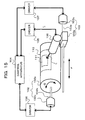
- Fig. 15 shows an optical diffraction structure production apparatus to be used in the embodiment.
- a laser irradiation apparatus 100 for irradiating with an IR laser L as energy beam a drum apparatus 102 for holding a master hologram, and a transportation apparatus 103 are connected to a control apparatus 104 for controlling the operation of the above-mentioned apparatuses through drivers 105, 106, and 107 respectively.
- the drum apparatus 102 is provided with a column type drum 102a and a motor 102c for rotating the drum 102a on the axis 102b in the direction Q.
- Small holes are formed in the entire outer circumferential face of the drum 102a and the air in the inside of the drum 102a is sucked by a suction pump (not shown), so that negative pressure is generated in the inside of the drum 102a to attach a master hologram 110 and a film 111 for hologram formation to the surface of the drum 102a.
- the respective structures of the master hologram 110 and the film 111 for hologram formation will be described later.
- the transportation apparatus 103 is provided with a transportation part 103 and a motor 103c for moving the transportation part 103a in the direction parallel to the axial direction of the drum 102a, that is in the direction shown by the arrow F, on a rail 103b. Since the laser irradiation apparatus 100 is set on the transportation part 103a, along with the transportation of the transportation part 103a, the laser irradiation apparatus 100 can move in parallel to the side face of the drum 102a.
- the laser irradiation apparatus 100 irradiates the master hologram 110 attached to the side face of the drum 102a with IR laser L.
- the irradiation region of the IR laser L in the master hologram 110 can be shifted by the parallel movement of the laser irradiation apparatus 100 by the above-mentioned transportation apparatus 103 and rotation of the drum 102a.
- the control apparatus 104 comprises a computer comprising a CPU and various peripheral circuits such as RAM and ROM necessary for the operation of the CPU and is employed to control the operations of the above-mentioned laser irradiation apparatus 100, drum apparatus 102, and transportation apparatus 103 according to previously installed programs. Accordingly, shift of the irradiation region of the IR laser L with which the master hologram 110 is irradiated by the laser irradiation apparatus 100 is controlled by the control apparatus 104.
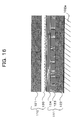
- Fig. 16 shows the state that master hologram 110 and the film 111 for forming hologram to be used in this embodiment are laminated on the outer circumference of the drum 102a.
- the master hologram 110 is provided with a hologram layer 120 in which the interference fringes are formed in concavo-convex form and a base substrate layer 121 of polyethylene terephthalate.
- the master hologram 110 can be produced by a conventionally known method.
- the hologram to be used for the hologram layer 120 may be those which can record hologram information by the concavo-convex form in the material surface and are applicable for a conventional method for copying hologram by using a thermoplastic resin.
- holograms based on the Fresnel hologram, Fourier transform hologram, Fraunhofer hologram; and holograms utilising their principles, such as image hologram, holographic stereogram, and holographic diffraction lattice can be used.
- a diffraction lattice having the concavo-convex patterns evenly formed therein may be used and, in this case, the lattice patterns of the diffraction lattice are transferred to the film 111 for forming hologram.
- the film 111 for forming the hologram is composed by layering a primer layer 123 and a fusible layer 124 on the base substrate layer 122 of polyethylene terephthalate.
- the fusible layer 124 comprises wax, a thermoplastic resin, and a high heat conversion material as a substance for increasing the conversion efficiency from light energy of IR laser to heat energy.
- the thermoplastic resin and wax composing the fusible layer 124 may be those which are solid state at a normal temperature.
- the primer layer 123 functions as a primer for sticking the base substrate layer 122 and the fusible layer 124 to each other.
- Fig. 17 the master hologram 110 and the film 111 for forming hologram are attached to the outer circumference of the drum 102a as described above.
- the master hologram 110 and the film 111 for forming the hologram are layered to each other and irradiated from the base substrate layer 121 side with the IR laser L moving in the direction shown by the arrow C.
- an irradiation region W1 of the fusible layer 124 is heated by the heat of the IR laser L.
- the fusible layer 124 in the range is fused and the interference fringes of the hologram layer 120 in the irradiation region W1 are transferred to the fusible layer 124.
- the IR laser L is shifted to an irradiation region W2.
- Fig. 17 shows the state that the interference fringes in the irradiation region W1 are transferred to the fusible layer 124 and the IR laser is shifted to the irradiation region W2.
- the temperature in the transferred range W1 of the fusible layer 124 decreases without a particular cooling process and the fused fusible layer 124 becomes cured.
- the fusible layer 124 in the range is fused and the interference fringes of the hologram layer 120 in the irradiation region W2 are transferred to the fusible layer 124.
- the interference fringes in the ranges which are irradiated with the IR laser L are successively transferred to the fusible layer 124.
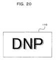
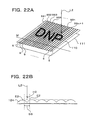
- interference fringes for producing letters "DNP" as hologram images are formed in the hologram layer 120 of the master hologram 110 in the embodiment, as shown in Fig. 20 .
- the object region for copying is the entire master hologram 110.
- the copying method for the optical diffraction structure comprises a first transfer process and a second transfer process.
- First, the first transfer process will be described.
- the master hologram 110 and the film 111 for forming the hologram are layered and set on the drum 102a with the film 111 for forming the hologram being set under.
- the master hologram 110 and the film 111 for forming hologram are attracted to and fixed in the side face of the drum 102a by the negative pressure generated in the inside of the drum 102a.
- the master hologram 110 is irradiated from the laser irradiation apparatus 100 with IR laser L1 in the first transfer process.
- the master hologram 110 is irradiated with the IR laser L1 so as to draw straight scanning lines S1...Sn (hereinafter, in the case that the lines need not be specially distinguished, referred simply to as "scanning lines S") in a lengthwise direction as a constant direction.
- the scanning lines S are drawn by shifting the irradiation region of the IR laser L1.
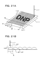
- Fig. 21A shows the state that the scanning lines S1 to Sn are already drawn and the scanning line Sn+1 is being drawn.
- the fusible layer 124 When the fusible layer 124 is irradiated with the IR laser L1, the light energy of the IR laser L1 is converted into heat energy to heat the irradiation region.
- the temperature of the irradiation region reaches the fusing point of the fusible layer 24, the irradiation region is fused and the interference fringes overlaid in the fused part are transferred. Accordingly, as the scanning lines S are drawn by the IR laser L1, that is, the irradiation region is shifted, the interference fringes in the irradiation region of the master hologram 110 are successively transferred to the fusible layer 124 of the film 111 for forming the hologram.
- the line width and the pitches of the scanning lines S are previously set to be 65 ⁇ m and 60 ⁇ m, respectively, in the optical diffraction structure copying apparatus, and the starting position and the finishing position of the respective scanning lines S are controlled based on the program taken in the control apparatus 104.
- the control apparatus 104 judges that the entire body of the master hologram 110 has been scanned by the IR laser L1, the first transfer process is finished.
- the scanning lines S are shown as visible lines for explanation convenience. However, the scanning lines are traces of the irradiation regions of the moving IR laser L1 and no visible line is actually drawn in the master hologram 110.
- Fig. 21B shows a cross-sectional view of the obtained film 111 for forming the hologram on completion of the first transfer process along the line M.
- a cyclic concavo-convex form is formed in the fusible layer 124.
- One rising part corresponds to the line width of one scanning line S.
- the highest part H1 is the centre part of the irradiation region of the IR laser L1.
- the lowest parts E1 are boundary parts of the irradiation region of the IR laser L1.
- the fusible layer 124 in the irradiation region is easily fused and the fusible layer 124 in the boundary parts are relatively hard to be fused. Accordingly, in the fusible layer 124 pressurised from the upper side by the master hologram 110, the part easy to be fused rises easily and the shape shown in Fig. 21B can be formed by drawing a plurality of scanning lines S in parallel.
- the master hologram 110 and the film 111 for forming the hologram may be as they are at the time of finishing the first transfer process.
- the boundary parts of the scanning lines S drawn in the first transfer process are irradiated with IR laser L2 to draw scanning lines SS1...SSn (hereinafter, in the case the lines need not be specially distinguished, referred simply to as "scanning lines SS") shown as dotted lines along with the scanning lines S.
- the scanning lines SS are drawn by shifting the irradiation region of the IR laser L2.
- the energy dose of the IR laser L2 is determined relative to the energy dose of the IR laser L1 and it may be in a range of 0.3 to 1 times as much as that of the IR laser L1. In this embodiment, the energy dose of the IR laser L2 is set so as to adjust the line width of the scanning lines SS to be 35 ⁇ m.
- the scanning lines SS are drawn, that is, with the shift of the irradiation region of the IR laser L2, because of the same reason as the principle described above, the interference fringes in the irradiation region of the master hologram 110 are successively transferred.
- the pitches and the line width of the scanning lines SS are previously set and the starting position and the finishing position of the respective scanning lines SS are controlled based on the program taken in the control apparatus 104.
- the control apparatus 104 judges that all of the boundary parts of the scanning lines S are scanned by the IR laser L2, the second transfer process is finished.
- the scanning lines SS are drawn as visible dotted lines for explanation convenience in Fig. 22A , the scanning lines SS are traces of the irradiation region of the moving IR laser L2 and no visible dotted line is drawn actually on the master hologram 110.
- Fig. 22B shows a cross-sectional view of the obtained film 111 for forming the hologram on completion of the second transfer process along the line M.
- a cyclic concavo-convex form shown with dotted lines is formed in the boundary parts of the scanning lines S.
- One rising part corresponds to the line width of one scanning line SS.
- the highest part H2 is the centre part of the irradiation region of the IR laser L2.
- the lowest parts E2 are boundary parts of the irradiation region of the IR laser L2.
- the highest part H2 is formed in the position of the lower parts E1 generated in the first transfer process, so that the height difference in the surface of the fusible layer 124 caused by the first transfer process can be amended. Accordingly, the surface of the fusible layer 124 of the film 111 for forming the hologram obtained after the second transfer process is provided with improved flatness compared to the surface of the fusible layer 124 of the film 111 for forming the hologram obtained after the first transfer process.
- the method for copying an optical diffraction structure is not limited to the above-mentioned embodiment and can be performed in various embodiments.
- master holograms 110...110 to express a plurality of hologram images or master holograms 110...110 of diffraction lattices may be combined and, according to the copying method as described above, they may be copied to one film 111 for forming the hologram.
- the film 111 for forming the hologram in which all of the master holograms 110...110 are copied is copied to an easily adhesive transparent PET film by the 2P copying method, by using this PET film as the hologram original forme, it is easy to copy the hologram to express a plurality of hologram images.
- other holograms and diffraction lattice patterns can be repeatedly arranged by the method.
- the scanning pitches employed at the initial arrangement are different from the scanning pitches employed at the second arrangement, for example, the scanning pitches of the first arrangement are adjusted to be 80 ⁇ m and the scanning pitches of the second arrangement are adjusted to be 60 ⁇ m
- vertical stripes (moires) are generated by the pitch of 240 ⁇ m which is lowest common multiple of 60 and 80.
- the vertical stripe (moires) formation can be prevented and, therefore, it is not necessary that the scanning pitches of the second arrangement are equal to the scanning pitches of the first arrangement. That is, there is an advantage that the scanning pitches are set freely.
- the energy dose of the IR laser L1 in the first transfer process may be set properly based on the raw materials and the depth of the hologram layer 120 and the fusible layer 124.
- the energy dose of the IR laser L2 may be set higher than that of the IR laser L1.
- the energy doses of the respective IR laser beams L1 and L2 may be adjusted so as to obtain the flatness of the surface of the fusible layer 124 of the finally obtained film 111 for forming hologram.
- the shifting speeds of the IR laser L1 and IR laser L2 may be set properly based on the raw materials of the fusible layer 124 and the depth of the interference fringes in the fusible layer 124 and the hologram layer 120 so as to heat the fusible layer 124 to the fusing point and then spontaneously cool the fusible layer 124 quickly.
- the copying method for obtaining the optical diffraction structure by two time transferring processes in total (the first transfer process and the second transfer process) is explained, and a third transfer process for irradiating the boundary parts of the scanning lines SS of the second transfer process with an IR laser having smaller energy dose than that of the IR laser L2 may be further added.
- transfer processes similar to the second transfer process may be carried out without any limit in the number of times of repeating the processes.
Landscapes
- Physics & Mathematics (AREA)
- Engineering & Computer Science (AREA)
- General Physics & Mathematics (AREA)
- Manufacturing & Machinery (AREA)
- Optics & Photonics (AREA)
- Mechanical Engineering (AREA)
- Diffracting Gratings Or Hologram Optical Elements (AREA)
- Holo Graphy (AREA)
- Shaping Of Tube Ends By Bending Or Straightening (AREA)
Claims (3)
- Verfahren zum Kopieren einer optischen Beugestruktur, wobei das Verfahren umfasst:- Laminieren einer Hologramm-Vorlage (100) für eine optische Beugestruktur mit einem auf eine Schmelzschicht (124) zu kopierenden, auf einem Grundsubstrat (122) ausgebildetem Merkmalsbereich, wobei die Hologramm-Vorlage für die optische Beugestruktur optische Interferenzränder von konkav-konvexer Form aufweist;- Bestrahlen der Hologramm-Vorlage (110) für die laminierte optische Beugestruktur und der Schmelzschicht (124) mit einem Energiestrahl (L, L1, L2) derart, dass ein Bestrahlungsbereich auf einen Anteil des zu kopierenden Merkmalsbereichs beschränkt bleibt, um die Schmelzschicht (124) in dem Bestrahlungsbereich mit der durch den Energiestrahl (L, L1, L2) eingebrachten Wärme zum Schmelzen zu bringen,
wobei eine Bestrahlung mit dem Energiestrahl eine Erhöhung des geschmolzenen Anteils bewirkt, und- sukzessives Übertragen der Interferenzränder auf die Schmelzschicht (124) durch Verschieben des Bestrahlungsbereichs in den zu kopierenden Merkmalsbereich,wobei der Schritt des Übertragens umfasst:- einen ersten Übertragungsvorgang des sukzessiven Übertragens der Interferenzränder auf die Schmelzschicht (124) durch Verschieben des Bestrahlungsbereichs des Energiestrahls (L1) längs eines vorgegebenen Pfades, um erste Abtastlinien (S) zu ziehen, und- einen zweiten Übertragungsvorgang des sukzessiven Übertragens der Interferenzränder in eine Grenzfläche (E1) an der weniger erhabenen Kante jeder ersten Abtastlinie (S), die in dem auf die Schmelzschicht (124) zu kopierenden Merkmalsbereich durch Bestrahlen der Grenzflächen (E1) mit dem Energiestrahl (L2) gezogen wird und Verschieben des Bestrahlungsbereichs des Energiestrahls (L2) längs der ersten Abtastlinien (S), um zweite Abtastlinien (SS) zu ziehen. - Verfahren nach Anspruch 1, wobei eine Energiedosis des Energiestrahls (L2) in dem zweiten Übertragungsvorgang gleich oder geringer als eine Energiedosis des Energiestrahls (L1) in dem ersten Übertragungsvorgang ist.
- Verfahren nach Anspruch 1, wobei eine Energiedosis des Energiestrahls (L2) in dem zweiten Übertragungsvorgang im Bereich von 0,3 bis zu dem Einfachen der Energiedosis des Energiestrahls (L1) in dem ersten Übertragungsvorgang liegt.
Priority Applications (1)
| Application Number | Priority Date | Filing Date | Title |
|---|---|---|---|
| EP07075288A EP1806635A3 (de) | 2003-09-17 | 2004-09-17 | Verfahren zur Herstellung feiner Konkav-Konvex-Muster, Verfahren zur Herstellung optischer Diffraktionsstrukturen und Verfahren zum Kopieren optischer Diffraktionsstrukturen |
Applications Claiming Priority (6)
| Application Number | Priority Date | Filing Date | Title |
|---|---|---|---|
| JP2003324608 | 2003-09-17 | ||
| JP2003324608 | 2003-09-17 | ||
| JP2003333170A JP4318996B2 (ja) | 2003-09-25 | 2003-09-25 | 光回折構造の製造方法 |
| JP2003333170 | 2003-09-25 | ||
| JP2003334750A JP4056957B2 (ja) | 2003-09-26 | 2003-09-26 | 光回折構造の複製方法 |
| JP2003334750 | 2003-09-26 |
Related Child Applications (2)
| Application Number | Title | Priority Date | Filing Date |
|---|---|---|---|
| EP07075288A Division EP1806635A3 (de) | 2003-09-17 | 2004-09-17 | Verfahren zur Herstellung feiner Konkav-Konvex-Muster, Verfahren zur Herstellung optischer Diffraktionsstrukturen und Verfahren zum Kopieren optischer Diffraktionsstrukturen |
| EP07075288.6 Division-Into | 2007-04-17 |
Publications (3)
| Publication Number | Publication Date |
|---|---|
| EP1519249A2 EP1519249A2 (de) | 2005-03-30 |
| EP1519249A3 EP1519249A3 (de) | 2006-06-28 |
| EP1519249B1 true EP1519249B1 (de) | 2012-07-11 |
Family
ID=34198765
Family Applications (2)
| Application Number | Title | Priority Date | Filing Date |
|---|---|---|---|
| EP07075288A Withdrawn EP1806635A3 (de) | 2003-09-17 | 2004-09-17 | Verfahren zur Herstellung feiner Konkav-Konvex-Muster, Verfahren zur Herstellung optischer Diffraktionsstrukturen und Verfahren zum Kopieren optischer Diffraktionsstrukturen |
| EP04255662A Expired - Lifetime EP1519249B1 (de) | 2003-09-17 | 2004-09-17 | Verfahren zum Kopieren von optischen Beugungstrukturen |
Family Applications Before (1)
| Application Number | Title | Priority Date | Filing Date |
|---|---|---|---|
| EP07075288A Withdrawn EP1806635A3 (de) | 2003-09-17 | 2004-09-17 | Verfahren zur Herstellung feiner Konkav-Konvex-Muster, Verfahren zur Herstellung optischer Diffraktionsstrukturen und Verfahren zum Kopieren optischer Diffraktionsstrukturen |
Country Status (2)
| Country | Link |
|---|---|
| US (2) | US7245406B2 (de) |
| EP (2) | EP1806635A3 (de) |
Families Citing this family (33)
| Publication number | Priority date | Publication date | Assignee | Title |
|---|---|---|---|---|
| US7245406B2 (en) * | 2003-09-17 | 2007-07-17 | Dai Nippon Printing Co., Ltd. | Method for forming fine concavo-convex patterns, method for producing optical diffraction structure, and method for copying optical diffraction structure |
| JP4826142B2 (ja) * | 2005-06-03 | 2011-11-30 | 大日本印刷株式会社 | 熱転写シートの製造方法及び熱転写方法 |
| US20070023976A1 (en) * | 2005-07-26 | 2007-02-01 | Asml Netherlands B.V. | Imprint lithography |
| DE102007042385A1 (de) * | 2007-09-04 | 2009-03-05 | Bundesdruckerei Gmbh | Verfahren und Vorrichtung zur individuellen holografischen Trommelbelichtung |
| DE102007042386A1 (de) * | 2007-09-04 | 2009-03-05 | Bundesdruckerei Gmbh | Verfahren und Vorrichtung zur individuellen farbigen holografischen Belichtung |
| EP2081192A1 (de) * | 2008-01-15 | 2009-07-22 | Sony DADC Austria AG | Verfahren zur Herstellung eines optischen Datenträgers |
| EP2588898A4 (de) * | 2010-07-01 | 2014-06-11 | Nanocomp Oy Ltd | Optisches übertragungselement, beleuchtungsanordnung und herstellungsverfahren |
| JP2012256021A (ja) * | 2011-05-17 | 2012-12-27 | Sony Corp | 体積型ホログラムおよびその製造方法ならびに回折光の波長スペクトラムの偏移方法 |
| WO2014086715A1 (de) * | 2012-12-04 | 2014-06-12 | Sectago Gmbh | Sicherheitseinrichtung |
| CN105339179B (zh) * | 2013-02-12 | 2018-06-22 | 赛克达戈有限公司 | 安全装置 |
| KR20140141815A (ko) * | 2013-05-31 | 2014-12-11 | 삼성전자주식회사 | 전자기기용 케이스 및 이의 표면 처리방법 |
| US10207531B2 (en) * | 2013-12-02 | 2019-02-19 | SECTAG GmbH | Security device |
| JP6609402B2 (ja) * | 2014-06-19 | 2019-11-20 | デクセリアルズ株式会社 | 光学フィルム及びその製造方法 |
| JP6221983B2 (ja) * | 2014-07-29 | 2017-11-01 | 株式会社デンソー | 輻射ヒータ装置 |
| US11211625B2 (en) | 2016-04-21 | 2021-12-28 | Fuelcell Energy, Inc. | Molten carbonate fuel cell anode exhaust post-processing for carbon dioxide |
| CN116435559A (zh) | 2016-04-29 | 2023-07-14 | 燃料电池能有限公司 | 甲烷化阳极废气以提高二氧化碳捕获 |
| GB2552551A (en) | 2016-07-29 | 2018-01-31 | Metamaterial Tech Inc | Metamaterial optical filter and method for producing the same |
| KR102064297B1 (ko) * | 2017-02-16 | 2020-01-09 | 삼성에스디아이 주식회사 | 감광성 수지 조성물, 이를 이용한 블랙 화소 격벽층 및 디스플레이 장치 |
| FI127799B (en) | 2017-06-02 | 2019-02-28 | Dispelix Oy | Process for producing a diffraction grating |
| JP7069168B2 (ja) * | 2017-07-20 | 2022-05-17 | 三井化学東セロ株式会社 | 電子装置の製造方法 |
| JP2021504736A (ja) * | 2017-11-21 | 2021-02-15 | アプライド マテリアルズ インコーポレイテッドApplied Materials,Incorporated | 導波結合器の製造方法 |
| KR102438014B1 (ko) | 2017-11-29 | 2022-08-31 | 어플라이드 머티어리얼스, 인코포레이티드 | 도파관 결합기들의 방향성 식각 제조 방법 |
| GB2574884A (en) * | 2018-06-22 | 2019-12-25 | Metamaterial Tech Inc | Spatially varying volume holographic gratings |
| CN109143437B (zh) * | 2018-10-12 | 2021-03-02 | 宁波源禄光电有限公司 | 一种机械切削-离子束刻蚀制备光栅方法 |
| KR20230070334A (ko) * | 2018-10-22 | 2023-05-22 | 데쿠세리아루즈 가부시키가이샤 | 원판, 원판의 제조 방법 및 전사물의 제조 방법 |
| WO2020112810A1 (en) | 2018-11-30 | 2020-06-04 | Exxonmobil Research And Engineering Company | Flow field baffle for molten carbonate fuel cell cathode |
| AU2019386065A1 (en) | 2018-11-30 | 2021-06-10 | ExxonMobil Technology and Engineering Company | Cathode collector structures for molten carbonate fuel cell |
| WO2020112895A1 (en) | 2018-11-30 | 2020-06-04 | Exxonmobil Research And Engineering Company | Reforming catalyst pattern for fuel cell operated with enhanced co2 utilization |
| DE102019110587A1 (de) * | 2019-04-24 | 2020-10-29 | HELLA GmbH & Co. KGaA | Vorrichtung zur Herstellung eines Replik-Hologramms, Replik-Hologramm sowie Beleuchtungsvorrichtung für ein Fahrzeug |
| EP4066300A1 (de) | 2019-11-26 | 2022-10-05 | ExxonMobil Technology and Engineering Company | Brennstoffzellenmodul und systeme damit |
| KR20250141258A (ko) | 2019-11-26 | 2025-09-26 | 엑손모빌 테크놀로지 앤드 엔지니어링 컴퍼니 | 병렬 유동을 위한 외부 매니폴드를 갖는 연료 전지 어셈블리 |
| CN115427347B (zh) | 2020-03-11 | 2024-01-02 | 燃料电池能有限公司 | 用于碳捕获的蒸汽甲烷重整单元 |
| EP4454872A1 (de) * | 2023-04-27 | 2024-10-30 | Essilor International | Verfahren zum bedrucken von ophthalmischen laminaten und resistzusammensetzung dafür |
Family Cites Families (27)
| Publication number | Priority date | Publication date | Assignee | Title |
|---|---|---|---|---|
| US4064205A (en) | 1974-07-02 | 1977-12-20 | Logetronics, Inc. | Method for making a printing plate from a porous substrate |
| JPS5565525A (en) * | 1978-11-13 | 1980-05-17 | Furukawa Kinzoku Kogyo Kk | Embossing of synthetic resin foam |
| JPS5999475A (ja) | 1982-11-29 | 1984-06-08 | Dainippon Printing Co Ltd | 回折格子付ホログラムの製造方法 |
| JPH0685103B2 (ja) | 1984-05-31 | 1994-10-26 | 大日本印刷株式会社 | ホログラムの複製方法 |
| CH664030A5 (de) | 1984-07-06 | 1988-01-29 | Landis & Gyr Ag | Verfahren zur erzeugung eines makroskopischen flaechenmusters mit einer mikroskopischen struktur, insbesondere einer beugungsoptisch wirksamen struktur. |
| US5164227A (en) * | 1987-06-19 | 1992-11-17 | Van Leer Metallized Products (Usa) Limited | Method for embossing a coated sheet with a diffraction or holographic pattern |
| ATE69407T1 (de) * | 1988-03-03 | 1991-11-15 | Landis & Gyr Betriebs Ag | Dokument. |
| JP2789599B2 (ja) | 1988-04-01 | 1998-08-20 | 凸版印刷株式会社 | ホログラム面付型の作製方法 |
| JP2570402B2 (ja) | 1988-09-30 | 1997-01-08 | 日本ビクター株式会社 | 光学式情報記録媒体成型装置 |
| US5232817A (en) * | 1990-12-21 | 1993-08-03 | Konica Corporation | Thermal transfer image receiving material and method for preparing therefrom a proof for printing |
| US5672410A (en) * | 1992-05-11 | 1997-09-30 | Avery Dennison Corporation | Embossed metallic leafing pigments |
| JPH0685103A (ja) | 1992-08-31 | 1994-03-25 | Kyocera Corp | 回路基板及び回路基板の電極形成方法 |
| JP3376022B2 (ja) | 1993-05-27 | 2003-02-10 | 大日本印刷株式会社 | ホログラム原版の作成方法および作成装置 |
| US6088161A (en) * | 1993-08-06 | 2000-07-11 | The Commonwealth Of Australia Commonwealth Scientific And Industrial Research Organization | Diffractive device having a surface relief structure which generates two or more diffraction images and includes a series of tracks |
| EP0665117A1 (de) * | 1994-01-31 | 1995-08-02 | Agfa-Gevaert N.V. | Thermisches Farbstoffübertragungsbild mit verbesserter Lichtechtheit |
| JP3703608B2 (ja) | 1997-06-30 | 2005-10-05 | 大日本印刷株式会社 | 計算機ホログラムおよびその作成方法 |
| CA2244324A1 (en) | 1997-08-04 | 1999-02-04 | Hsm Holographic Systems Munchen Gmbh | A method and an apparatus for fabricating a surface structure, particularly a holographic surface structure, on a substrate |
| DE19746268A1 (de) * | 1997-10-20 | 1999-04-22 | Giesecke & Devrient Gmbh | Verfahren und Vorrichtung zur Herstellung eines Folienmaterials |
| JP2000221312A (ja) * | 1999-01-28 | 2000-08-11 | Idemitsu Petrochem Co Ltd | 再帰反射性シート |
| JP4363727B2 (ja) | 1999-12-02 | 2009-11-11 | 晏夫 黒崎 | プラスチック成形加工方法 |
| JP2001328354A (ja) * | 2000-05-19 | 2001-11-27 | Fuji Photo Film Co Ltd | 熱転写シートおよび熱転写記録方法 |
| US6616867B2 (en) * | 2001-02-07 | 2003-09-09 | Imation Corp. | Multi-generation stampers |
| US20040150135A1 (en) * | 2002-06-26 | 2004-08-05 | Michael Hennessey | Method of melt-forming optical disk substrates |
| JP2005005245A (ja) * | 2002-11-08 | 2005-01-06 | Fuji Photo Film Co Ltd | 転写素材の転写方法、形状転写方法及び転写装置 |
| EP1627261B1 (de) * | 2003-04-10 | 2015-12-09 | Ronald R. Erickson | Eingebetteter informationsträger für optische daten |
| US7245406B2 (en) * | 2003-09-17 | 2007-07-17 | Dai Nippon Printing Co., Ltd. | Method for forming fine concavo-convex patterns, method for producing optical diffraction structure, and method for copying optical diffraction structure |
| JP2005231231A (ja) * | 2004-02-20 | 2005-09-02 | Konica Minolta Medical & Graphic Inc | 印刷版材料 |
-
2004
- 2004-09-16 US US10/942,296 patent/US7245406B2/en not_active Expired - Lifetime
- 2004-09-17 EP EP07075288A patent/EP1806635A3/de not_active Withdrawn
- 2004-09-17 EP EP04255662A patent/EP1519249B1/de not_active Expired - Lifetime
-
2007
- 2007-06-18 US US11/764,266 patent/US7955785B2/en not_active Expired - Fee Related
Also Published As
| Publication number | Publication date |
|---|---|
| EP1519249A3 (de) | 2006-06-28 |
| US7245406B2 (en) | 2007-07-17 |
| EP1519249A2 (de) | 2005-03-30 |
| US20070243475A1 (en) | 2007-10-18 |
| US7955785B2 (en) | 2011-06-07 |
| US20050057789A1 (en) | 2005-03-17 |
| EP1806635A3 (de) | 2011-03-09 |
| EP1806635A2 (de) | 2007-07-11 |
Similar Documents
| Publication | Publication Date | Title |
|---|---|---|
| EP1519249B1 (de) | Verfahren zum Kopieren von optischen Beugungstrukturen | |
| JP4635006B2 (ja) | シリンダ形プラットフォームおよびラスタ走査される放射線ビームを使用して光学的微細構造体を形成するためのシステムおよび方法 | |
| JP2007507725A (ja) | シリンダ形プラットフォームおよびラスタ走査される放射線ビームを使用して光学的微細構造体を形成するためのシステムおよび方法 | |
| JP2007507364A (ja) | 外層の間に挟み込まれた放射線感応層を結像処理することによって微細構造体を形成するためのシステムおよび方法並びにそれにより形成された微細構造体 | |
| JP5703600B2 (ja) | インプリント用モールド、アライメント方法、インプリント方法、およびインプリント装置 | |
| WO1994004948A1 (en) | Apparatus for providing autostereoscopic and dynamic images and method of manufacturing same | |
| CN100384616C (zh) | 在底物上制造标记的设备和方法 | |
| US20070003876A1 (en) | Microstructure and method for producing microstructures | |
| JP2005103991A (ja) | 複製版の製造方法 | |
| EP1974241A1 (de) | Optisch variable sicherheitsvorrichtung | |
| CN100386654C (zh) | 微结构及其微结构产生的工艺 | |
| JP2005535483A (ja) | レーザー支援複製プロセス | |
| JP4056957B2 (ja) | 光回折構造の複製方法 | |
| JP4318996B2 (ja) | 光回折構造の製造方法 | |
| US20040121246A1 (en) | Lithography process to reduce seam lines in an array of microelements produced from a sub-mask and a sub-mask for use thereof | |
| JPS58144877A (ja) | ホログラムの複製方法 | |
| JP2014151446A (ja) | モアレ模様装飾体、モアレ模様装飾体の製造方法及びモアレ模様装飾体を用いた偽造防止部材 | |
| JP2004042475A (ja) | マイクロレンズアレイシート用ロールスタンパの製造方法 | |
| JP2015092599A (ja) | インプリント用モールド、アライメント方法、インプリント方法、およびインプリント装置 | |
| JPS58144878A (ja) | ホログラムの複製方法 | |
| JPH04151188A (ja) | レリーフパターンの複製方法 | |
| JP6197900B2 (ja) | インプリント用モールド、アライメント方法、インプリント方法、およびインプリント装置 | |
| JP2006335006A (ja) | 熱転写シートの製造方法及び熱転写方法 | |
| JP2007212575A (ja) | 光回折素子、光線走査方法、光線走査装置及び画像形成装置 | |
| JPH0368986A (ja) | エンボスロールの作成方法 |
Legal Events
| Date | Code | Title | Description |
|---|---|---|---|
| PUAI | Public reference made under article 153(3) epc to a published international application that has entered the european phase |
Free format text: ORIGINAL CODE: 0009012 |
|
| AK | Designated contracting states |
Kind code of ref document: A2 Designated state(s): AT BE BG CH CY CZ DE DK EE ES FI FR GB GR HU IE IT LI LU MC NL PL PT RO SE SI SK TR |
|
| AX | Request for extension of the european patent |
Extension state: AL HR LT LV MK |
|
| PUAL | Search report despatched |
Free format text: ORIGINAL CODE: 0009013 |
|
| AK | Designated contracting states |
Kind code of ref document: A3 Designated state(s): AT BE BG CH CY CZ DE DK EE ES FI FR GB GR HU IE IT LI LU MC NL PL PT RO SE SI SK TR |
|
| AX | Request for extension of the european patent |
Extension state: AL HR LT LV MK |
|
| 17P | Request for examination filed |
Effective date: 20060912 |
|
| 17Q | First examination report despatched |
Effective date: 20061013 |
|
| AKX | Designation fees paid |
Designated state(s): DE FR GB |
|
| GRAP | Despatch of communication of intention to grant a patent |
Free format text: ORIGINAL CODE: EPIDOSNIGR1 |
|
| RTI1 | Title (correction) |
Free format text: METHOD FOR COPYING OPTICAL DIFFRACTION STRUCTURES |
|
| RIN1 | Information on inventor provided before grant (corrected) |
Inventor name: FUNADA, HIROSHIDAI NIPPON PRINTING CO. LTD. Inventor name: MATSUYAMA, TETSUYADAI NIPPON PRINTING CO. LTD. Inventor name: MIZUKAMI, FUMIHIKODAI NIPPON PRINTING CO. LTD. |
|
| RAP1 | Party data changed (applicant data changed or rights of an application transferred) |
Owner name: DAI NIPPON PRINTING CO., LTD. |
|
| GRAS | Grant fee paid |
Free format text: ORIGINAL CODE: EPIDOSNIGR3 |
|
| GRAA | (expected) grant |
Free format text: ORIGINAL CODE: 0009210 |
|
| AK | Designated contracting states |
Kind code of ref document: B1 Designated state(s): DE FR GB |
|
| REG | Reference to a national code |
Ref country code: GB Ref legal event code: FG4D |
|
| REG | Reference to a national code |
Ref country code: DE Ref legal event code: R096 Ref document number: 602004038487 Country of ref document: DE Effective date: 20120906 |
|
| PLBE | No opposition filed within time limit |
Free format text: ORIGINAL CODE: 0009261 |
|
| STAA | Information on the status of an ep patent application or granted ep patent |
Free format text: STATUS: NO OPPOSITION FILED WITHIN TIME LIMIT |
|
| 26N | No opposition filed |
Effective date: 20130412 |
|
| REG | Reference to a national code |
Ref country code: DE Ref legal event code: R097 Ref document number: 602004038487 Country of ref document: DE Effective date: 20130412 |
|
| REG | Reference to a national code |
Ref country code: FR Ref legal event code: PLFP Year of fee payment: 13 |
|
| REG | Reference to a national code |
Ref country code: FR Ref legal event code: PLFP Year of fee payment: 14 |
|
| REG | Reference to a national code |
Ref country code: FR Ref legal event code: PLFP Year of fee payment: 15 |
|
| PGFP | Annual fee paid to national office [announced via postgrant information from national office to epo] |
Ref country code: FR Payment date: 20200914 Year of fee payment: 17 Ref country code: GB Payment date: 20200922 Year of fee payment: 17 Ref country code: DE Payment date: 20200925 Year of fee payment: 17 |
|
| REG | Reference to a national code |
Ref country code: DE Ref legal event code: R119 Ref document number: 602004038487 Country of ref document: DE |
|
| GBPC | Gb: european patent ceased through non-payment of renewal fee |
Effective date: 20210917 |
|
| PG25 | Lapsed in a contracting state [announced via postgrant information from national office to epo] |
Ref country code: GB Free format text: LAPSE BECAUSE OF NON-PAYMENT OF DUE FEES Effective date: 20210917 Ref country code: FR Free format text: LAPSE BECAUSE OF NON-PAYMENT OF DUE FEES Effective date: 20210930 Ref country code: DE Free format text: LAPSE BECAUSE OF NON-PAYMENT OF DUE FEES Effective date: 20220401 |