EP1515342A1 - Demodulator sowie diesen enthaltenes Datenaufzeichnungsgerät - Google Patents
Demodulator sowie diesen enthaltenes Datenaufzeichnungsgerät Download PDFInfo
- Publication number
- EP1515342A1 EP1515342A1 EP04104234A EP04104234A EP1515342A1 EP 1515342 A1 EP1515342 A1 EP 1515342A1 EP 04104234 A EP04104234 A EP 04104234A EP 04104234 A EP04104234 A EP 04104234A EP 1515342 A1 EP1515342 A1 EP 1515342A1
- Authority
- EP
- European Patent Office
- Prior art keywords
- signal
- synchronization signal
- bit
- bit synchronization
- value
- Prior art date
- Legal status (The legal status is an assumption and is not a legal conclusion. Google has not performed a legal analysis and makes no representation as to the accuracy of the status listed.)
- Granted
Links
Images


Classifications
-
- H—ELECTRICITY
- H02—GENERATION; CONVERSION OR DISTRIBUTION OF ELECTRIC POWER
- H02J—ELECTRIC POWER NETWORKS; CIRCUIT ARRANGEMENTS OR SYSTEMS FOR SUPPLYING OR DISTRIBUTING ELECTRIC POWER; SYSTEMS FOR STORING ELECTRIC ENERGY
- H02J7/00—Circuit arrangements for charging or discharging batteries or for supplying loads from batteries
- H02J7/60—Circuit arrangements for charging or discharging batteries or for supplying loads from batteries including safety or protection arrangements
- H02J7/64—Circuit arrangements for charging or discharging batteries or for supplying loads from batteries including safety or protection arrangements against overvoltage
-
- G—PHYSICS
- G11—INFORMATION STORAGE
- G11B—INFORMATION STORAGE BASED ON RELATIVE MOVEMENT BETWEEN RECORD CARRIER AND TRANSDUCER
- G11B27/00—Editing; Indexing; Addressing; Timing or synchronising; Monitoring; Measuring tape travel
- G11B27/10—Indexing; Addressing; Timing or synchronising; Measuring tape travel
- G11B27/19—Indexing; Addressing; Timing or synchronising; Measuring tape travel by using information detectable on the record carrier
- G11B27/24—Indexing; Addressing; Timing or synchronising; Measuring tape travel by using information detectable on the record carrier by sensing features on the record carrier other than the transducing track ; sensing signals or marks recorded by another method than the main recording
-
- G—PHYSICS
- G11—INFORMATION STORAGE
- G11B—INFORMATION STORAGE BASED ON RELATIVE MOVEMENT BETWEEN RECORD CARRIER AND TRANSDUCER
- G11B20/00—Signal processing not specific to the method of recording or reproducing; Circuits therefor
- G11B20/10—Digital recording or reproducing
- G11B20/10009—Improvement or modification of read or write signals
-
- G—PHYSICS
- G11—INFORMATION STORAGE
- G11B—INFORMATION STORAGE BASED ON RELATIVE MOVEMENT BETWEEN RECORD CARRIER AND TRANSDUCER
- G11B20/00—Signal processing not specific to the method of recording or reproducing; Circuits therefor
- G11B20/10—Digital recording or reproducing
- G11B20/14—Digital recording or reproducing using self-clocking codes
- G11B20/1403—Digital recording or reproducing using self-clocking codes characterised by the use of two levels
-
- G—PHYSICS
- G11—INFORMATION STORAGE
- G11B—INFORMATION STORAGE BASED ON RELATIVE MOVEMENT BETWEEN RECORD CARRIER AND TRANSDUCER
- G11B7/00—Recording or reproducing by optical means, e.g. recording using a thermal beam of optical radiation by modifying optical properties or the physical structure, reproducing using an optical beam at lower power by sensing optical properties; Record carriers therefor
- G11B7/004—Recording, reproducing or erasing methods; Read, write or erase circuits therefor
- G11B7/005—Reproducing
- G11B7/0053—Reproducing non-user data, e.g. wobbled address, prepits, BCA
-
- H—ELECTRICITY
- H01—ELECTRIC ELEMENTS
- H01M—PROCESSES OR MEANS, e.g. BATTERIES, FOR THE DIRECT CONVERSION OF CHEMICAL ENERGY INTO ELECTRICAL ENERGY
- H01M10/00—Secondary cells; Manufacture thereof
- H01M10/42—Methods or arrangements for servicing or maintenance of secondary cells or secondary half-cells
- H01M10/44—Methods for charging or discharging
- H01M10/441—Methods for charging or discharging for several batteries or cells simultaneously or sequentially
-
- H—ELECTRICITY
- H02—GENERATION; CONVERSION OR DISTRIBUTION OF ELECTRIC POWER
- H02J—ELECTRIC POWER NETWORKS; CIRCUIT ARRANGEMENTS OR SYSTEMS FOR SUPPLYING OR DISTRIBUTING ELECTRIC POWER; SYSTEMS FOR STORING ELECTRIC ENERGY
- H02J7/00—Circuit arrangements for charging or discharging batteries or for supplying loads from batteries
- H02J7/50—Circuit arrangements for charging or discharging batteries or for supplying loads from batteries acting upon multiple batteries simultaneously or sequentially
- H02J7/52—Circuit arrangements for charging or discharging batteries or for supplying loads from batteries acting upon multiple batteries simultaneously or sequentially for charge balancing, e.g. equalisation of charge between batteries
- H02J7/54—Passive balancing, e.g. using resistors or parallel MOSFETs
-
- H—ELECTRICITY
- H02—GENERATION; CONVERSION OR DISTRIBUTION OF ELECTRIC POWER
- H02J—ELECTRIC POWER NETWORKS; CIRCUIT ARRANGEMENTS OR SYSTEMS FOR SUPPLYING OR DISTRIBUTING ELECTRIC POWER; SYSTEMS FOR STORING ELECTRIC ENERGY
- H02J7/00—Circuit arrangements for charging or discharging batteries or for supplying loads from batteries
- H02J7/60—Circuit arrangements for charging or discharging batteries or for supplying loads from batteries including safety or protection arrangements
- H02J7/61—Circuit arrangements for charging or discharging batteries or for supplying loads from batteries including safety or protection arrangements against overcharge
-
- H—ELECTRICITY
- H02—GENERATION; CONVERSION OR DISTRIBUTION OF ELECTRIC POWER
- H02J—ELECTRIC POWER NETWORKS; CIRCUIT ARRANGEMENTS OR SYSTEMS FOR SUPPLYING OR DISTRIBUTING ELECTRIC POWER; SYSTEMS FOR STORING ELECTRIC ENERGY
- H02J7/00—Circuit arrangements for charging or discharging batteries or for supplying loads from batteries
- H02J7/60—Circuit arrangements for charging or discharging batteries or for supplying loads from batteries including safety or protection arrangements
- H02J7/63—Circuit arrangements for charging or discharging batteries or for supplying loads from batteries including safety or protection arrangements against overdischarge
-
- G—PHYSICS
- G11—INFORMATION STORAGE
- G11B—INFORMATION STORAGE BASED ON RELATIVE MOVEMENT BETWEEN RECORD CARRIER AND TRANSDUCER
- G11B2220/00—Record carriers by type
- G11B2220/20—Disc-shaped record carriers
- G11B2220/21—Disc-shaped record carriers characterised in that the disc is of read-only, rewritable, or recordable type
- G11B2220/215—Recordable discs
- G11B2220/216—Rewritable discs
-
- G—PHYSICS
- G11—INFORMATION STORAGE
- G11B—INFORMATION STORAGE BASED ON RELATIVE MOVEMENT BETWEEN RECORD CARRIER AND TRANSDUCER
- G11B2220/00—Record carriers by type
- G11B2220/20—Disc-shaped record carriers
- G11B2220/25—Disc-shaped record carriers characterised in that the disc is based on a specific recording technology
- G11B2220/2537—Optical discs
- G11B2220/2562—DVDs [digital versatile discs]; Digital video discs; MMCDs; HDCDs
-
- Y—GENERAL TAGGING OF NEW TECHNOLOGICAL DEVELOPMENTS; GENERAL TAGGING OF CROSS-SECTIONAL TECHNOLOGIES SPANNING OVER SEVERAL SECTIONS OF THE IPC; TECHNICAL SUBJECTS COVERED BY FORMER USPC CROSS-REFERENCE ART COLLECTIONS [XRACs] AND DIGESTS
- Y02—TECHNOLOGIES OR APPLICATIONS FOR MITIGATION OR ADAPTATION AGAINST CLIMATE CHANGE
- Y02E—REDUCTION OF GREENHOUSE GAS [GHG] EMISSIONS, RELATED TO ENERGY GENERATION, TRANSMISSION OR DISTRIBUTION
- Y02E60/00—Enabling technologies; Technologies with a potential or indirect contribution to GHG emissions mitigation
- Y02E60/10—Energy storage using batteries
Definitions
- the present invention pertains to a demodulator for a phase modulated signal and a data recorder containing said demodulator.
- the present invention pertains to a demodulator for demodulating the wobble signal of an optical disk and a data recorder for said optical disk.
- the recording surface of a recordable optical disk contains a pre-formed guide groove in the shape of a spiral to ensure that the laser beam can correctly follow the recording track during writing.
- the edges of the guide groove describe a periodic undulation or wobble.
- the laser beam is irradiated on the edges, the reflected light is converted into an electronic signal, so that a periodic signal (wobble signal) corresponding to the wobble is obtained.
- the write signal may be used as the control signal.
- the optical disk is rotated at a constant linear velocity, it is used to generate the clock signal for write processing.
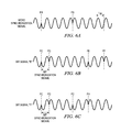
- the wobble signal of the DVD+RW format will be explained below with reference to the waveform diagram shown in FIG. 6.
- the wobble signal of the DVD+RW format is a signal in which the carrier component is phase-modulated to correspond to the address information known as ADIP (address in pre-groove).
- 93 wobble periods (93Tw) form a data wobble unit
- 52 data wobble units form one ADIP word.
- the bit synchronization signal for determining the starting point is inserted at the head of each data wobble unit. As shown in FIGS. 6(B) and (C), the bit synchronization signal is characterized by two phase change points (PC, PD) separated by one wobble period (1Tw).
- bit synchronization signal After the bit synchronization signal, a bit signal having different signal pattern corresponding to the bit value is inserted.
- the "0" bit signal is characterized by phase change point PE, which is six wobble periods (6Tw) from the initial phase change point PC of the bit synchronization signal, and by phase change point PF, which is two wobble periods (2Tw) from said phase change point PE.
- the "1" bit signal is characterized by phase change point PG, which is four wobble periods (4Tw) from the initial phase change point PC of the bit synchronization signal, and by phase change point PH, which is two wobble periods (2Tw) from said phase change point PG.
- the remaining periods of the data wobble unit (85Tw) is composed of a signal pattern with a single phase that does not contain a phase change point.
- the word synchronization signal is inserted in place of said bit synchronization signal and bit signal in the head data wobble unit in the 1ADIP word.
- the word synchronization signal is characterized by two phase change points (PA, PB) separated by 4 wobble periods (4Tw).
- the synchronization detection method is typically used to demodulate said phase modulated signal, wherein the phase modulated signal and its carrier component are multiplied. That is, the sinusoidal signal synchronized to the carrier component of the phase-modulated signal is reproduced and multiplied by the phase-modulated signal. Then, the product is low pass-filtered, and the positive/negative sign of the result is determined.
- Another method of demodulating the phase modulated signal is the method described in Patent Reference 1.
- the integration value of the phase modulated signal is compared with a threshold value. That is, a timing signal synchronized to the carrier component of the phase modulated signal is generated, and the integration value is computed for each full-period and half-period of the phase modulated signal.
- the modulated signal is demodulated to determine its value ("0" or "1").
- Patent Reference 1 Japanese Kokai Patent Application No. 2001-209937
- the value of the demodulation signal is judged by comparing the results obtained by multiplication, integration, etc. of phase modulated signal with a fixed threshold value. Consequently, when noise is superimposed on the phase modulated signal, the waveform collapses, and errors may easily take place in the judgment, which is undesirable.
- the purpose of the present invention is to solve the aforementioned problems of the conventional methods by providing a demodulator for phase modulated signals that can suppress an increase in the demodulation errors due to superimposed noise.
- Another purpose of the present invention is to provide a data recorder that can reliably write data with few errors to the recording medium through the incorporation of said demodulator.
- the demodulator is used to demodulate a phase modulated signal containing a bit synchronization signal that is inserted periodically and a bit signal that is inserted synchronously with said bit synchronization signal and that has a signal pattern corresponding to the bit value
- the demodulator is comprised of the following means: a carrier reproduction means that reproduces the carrier component of said phase modulated signal, an integration value computation means that computes the integration value over one period of said phase modulated signal or the integration values over plural sequential periods synchronously with said reproduced carrier component, a bit synchronization signal detection means that detects said bit synchronization signal inserted in said phase modulated signal, a bit signal characteristic quantity computation means that computes for each said bit value the characteristic quantity of said bit signal corresponding to the sum obtained after assigning prescribed signs to said integration values, respectively, during the periods where a change in phase of said bit synchronization signal in the signal range of said bit signal
- Said bit synchronization signal detection means may have a bit synchronization signal characteristic quantity computation means that computes the characteristic quantity of said bit synchronization signal corresponding to the sum obtained after assigning the prescribed signs to said integration values, respectively, during the periods where a change in phase of said bit synchronization signal in the signal range of said bit synchronization signal obtained by insertion in said phase modulated signal should take place, a threshold setting means that sets the threshold corresponding to the peak value and average value of said computed characteristic quantity of bit synchronization signal, and a first bit synchronization signal judgment means that compares said computed characteristic quantity of bit synchronization signal with said set threshold, and determines whether the signal of said signal range is said bit synchronization signal on the basis of said comparison result.
- said demodulator described may have a word synchronization signal detection means, which detects the word synchronization signal inserted periodically in said phase modulated signal in place of said bit synchronization signal.
- Said word synchronization signal detection means may contain a synchronization signal characteristic quantity computation means that computes the characteristic quantity of said word synchronization signal corresponding to the sum obtained after assigning the prescribed signs to said integration values, respectively, during the periods where a change in phase of said word synchronization signal should take place in the signal range of said word synchronization signal that can be inserted in place of said detected bit synchronization signal, and a first word synchronization signal judgment means that compares said computed characteristic quantity of word synchronization signal and said computed characteristic quantity of bit synchronization signal, and determines whether the signal of the signal range is said word synchronization signal on the basis of the result of said comparison.
- said carrier reproduction means may have a delay signal generating means that generates plural delay signals for establishing plural delays corresponding to the integer multiple of the period of said carrier component in said phase modulated signal, and an adder means that adds the plural delay signals generated by said delay signal generating means.
- the second invention for realizing said purpose provides a data recorder which contains a demodulator, which is used to demodulate a phase modulated signal pre-recorded on a recording medium and containing a bit synchronization signal that is inserted periodically and a bit signal that is inserted synchronously with said bit synchronization signal and that has a signal pattern corresponding to the bit value, wherein the data recorder uses the demodulation result of said demodulator to write data to said recording medium.
- Said demodulator is comprised of the following means: a carrier reproduction means that reproduces the carrier component of said phase modulated signal, an integration value computation means that computes the integration value over one period of said phase modulated signal or the integration values of plural sequential periods synchronously with said reproduced carrier component, a bit synchronization signal detection means that detects said bit synchronization signal inserted in said phase modulated signal, a bit signal characteristic quantity computation means that computes for each said bit value the characteristic quantity of said bit signal corresponding to the sum obtained after assigning prescribed signs to said integration values, respectively, during the periods where a change in phase of said bit synchronization signal should take place in the signal range of said bit signal obtained by insertion synchronously with said detected bit synchronization signal, and a bit value judging means that compares the characteristic quantities of said computed bit values, and determines the bit value of said bit signal on the basis of the comparison result.
- the demodulator of the present invention makes it possible to suppress increases in the demodulation error when the waveform of the phase modulated signal collapses due to the superimposition of noise in the signal.
- FIG. 1 is a block diagram illustrating an example of constitution of the data recording/reproduction device pertaining to an embodiment of the present invention.
- the data recording/reproduction device shown as example in FIG. 1 has the following parts: optical pickup 2, analog front end part 3, clock reproduction part 4, read data decoding part 5, wobble demodulator 6, wobble decoding part 7, write data encoding part 8, write clock generating part 9, write pulse generating part 10, laser driving part 11, interface part 12, servo-controller 13, actuator driving part 14, rotary motor driver 15, and disk motor 16.
- wobble demodulator 6 as an embodiment of the demodulator of the present invention.
- optical pickup 2 when data written in optical disk 1 is read, a laser beam for data read and for generating control signal is irradiated on the recording surface of optical disk 1, and the light reflected from the recording surface is converted into an electronic signal. Also, when data is written in optical disk 1, a laser beam for writing to the recording surface of optical disk 1 is irradiated to write the data, and at the same time, the laser beam for generating the control signal is irradiated and the reflected light is converted into an electronic signal.
- analog front end part 3 the electronic signal converted from the reflected light in optical pickup 2 undergoes digitization, wave-shaping, A/D conversion, and other signal processes to reproduce the read bit row corresponding to the channel bits on the recording track of optical disk 1. Also, various control signals are generated by said signal processing.
- control signals generated by analog front end part 3 include the wobble signal which corresponds to the wobble structure of the optical disk, the tracking error signal, which indicates the tracking error when the data recording track of the optical disk is tracked, the focusing error signal, which is used to maintain a constant focal distance between optical disk 1 and optical pickup 2, etc.
- clock reproduction part 4 reproduces the read clock signal as the reference of timing during the read processing.
- Read data decoding part 5 performs the prescribed decoding process for the read bit row output from analog front end part 3 and reproduces the read data synchronously with the read clock signal reproduced by the clock reproduction part.
- the reproduced read data is transferred via interface part 12 to the computer or other host device.
- wobble reproduction part 6 reproduces wobble clock signal CKw. Also, it performs demodulation of the wobble signal synchronously with said wobble clock signal CKw.
- wobble demodulator 6 The detailed constitution of wobble demodulator 6 will be explained below with reference to FIGS. 2-4.
- Wobble decoding part 7 performs the prescribed decoding processing for the signal that has been demodulated by wobble demodulator 6.
- Write data encoding part 8 performs the prescribed encoding treatment for the write data sent from the computer or other host device via interface part 12 synchronously with the write clock signal (to be explained below), and generates a write pulse row corresponding to the channel bit on the recording track of optical disk 1.
- Write clock generating part 9 multiplies the wobble clock signal CKw reproduced from the wobble signal in wobble reproduction part 6 by a prescribed multiplier ratio to generate the write clock signal as a timing reference for the write process.
- the write pulse row output from write data encoding part 8 is input to write pulse generating part 10 and processed corresponding to the type of disk to implement a write instruction from a controller (not shown in the figure). In this way, an appropriate write pulse signal corresponding to the type of optical disk is generated and is output to laser driving part 11.
- Laser driving part 11 generates a signal for driving the laser source of optical pickup 2 corresponding to the write pulse signal output from write pulse generating part 10, and generates a laser beam for writing data.
- Interface part 12 communicates with the host device (not shown in the figure) and retrieves write data and read data on the basis of ATAPI (AT attachment packet interface) or another interface format.
- ATAPI AT attachment packet interface
- servo-controller 13 Based on the tracking error signal, focus error signal, and other control signals output from analog front end part 3, servo-controller 13 generates signals for controlling the drive signals output from actuator drive part 14 and rotary motor driver 15, so that the laser beam of optical pickup 2 is irradiated at the assigned position on optical disk 1.
- servo-controller 13 may be a DSP (digital signal processor) or another processor.
- Actuator drive part 14 generates a signal for driving the actuator (not shown in the figure) that drives optical pickup 2 to move in accordance with to the control signal from servo-controller 13.
- Rotary motor driver 15 generates a signal for driving disk motor 16 corresponding to the control signal from servo-controller 13.
- Disk motor 16 drives optical disk 1 to rotate with a certain torque that is generated in accordance with the drive signal supplied from rotary motor driver 15.
- FIG. 2 is a block diagram illustrating an example constitution of pre-processor 61 of wobble demodulator 6.
- This pre-processor 61 is a unit that performs sampling rate conversion, offset removal, gain control, and other processes on the wobble signal output from analog front end part 3.
- Pre-processor 61 shown as an example in FIG. 2 has sampling rate converter 601, offset detection part 602, offset removal part 603, and gain controller 604.
- Sampling rate converter 601 converts the sampling rate of the wobble signal, which has been sampled at a lower rate than that of the write clock signal in analog front end part 3, into the same rate as the write clock signal.
- the bit rate of the channel rate is about 26.16 Mbps in the case of X1-speed write operation, and is over 200 Mbps in the case of X8-speed write operation.
- the analog/digital conversion rate in analog front end part 3 is set to about 100 Mbps, e.g. and X2 sampling rate conversion is performed in sampling rate converter 601. In this way, the analog/digital conversion speed is suppressed, so that the analog/digital converter can be simplified.
- the wobble signal after the rate conversion is performed by said sampling rate converter 601 is output to offset detection part 602 synchronously with the write clock signal of write clock signal generating part 9 that has the same frequency as that of the channel bit.
- Offset detection part 602 detects the low-frequency offset component in the wobble signal that has undergone rate conversion by sampling rate converter 601.
- offset detection part 602 may be realized with an IIR (infinite impulse response) filter or other filter circuit.
- IIR infinite impulse response
- filter circuit By setting the coefficients of the coefficient multiplication part of the filter circuit to an appropriate value, such as a power of 2 or its reciprocal, or a multiple of a power of 2 or its reciprocal, etc., it is possible to replace the multiplication operation in the coefficient multiplication part with a simpler operation, such as a bit shift, addition/subtraction, etc.
- Offset removal part 603 removes the offset component detected by offset detection part 602 from the wobble signal that has undergone rate conversion by sampling rate converter 601.
- the wobble signal, from which the offset component has been removed by offset detection part 603, is input to gain controller 604, which amplifies it; the gain is controlled such that the amplitude of the output signal is constant. Also, when the amplitude of the input wobble signal exceeds a prescribed level due to presence of scratches on the recording surface of the optical disk or for some other reason, the amplitude of the output signal will be limited to a prescribed upper limit level.
- gain controller 604 By setting an appropriate gain value of gain controller 604, such as a power of 2 or its reciprocal, or a multiple of a power of 2 or its reciprocal, etc., it is possible to replace the multiplication processing of gain controller 604 with a simpler operation, such as bit shift, addition/subtraction, etc.
- FIG. 3 is a block diagram illustrating an example constitution of demodulation processor 62 of wobble demodulator 6.
- Demodulation processor 62 demodulates wobble signal Sout, which has been subject to offset removal, and other processes in pre-processor 61, and outputs bit synchronization signal Bsync, word synchronization signal Wsync, and bit signal Bdat.
- wobble signal Sout demodulated by demodulation processor 62 is the phase demodulated signal ADIP shown in FIG. 6. Also, period Tw of wobble signal Sout is 32 times the period T of the channel bit.
- Demodulation processor 62 shown as an example in FIG. 3 includes adder 606, subtractors 610, 620, 627, 630, flip-flops 607-609, 618, 619, 625, 626, 628, 629, peak value computation unit 611, average value computation unit 612, threshold setting part 613, first bit synchronization signal judgment part 614, second bit synchronization signal judgment part 615, first word synchronization judgment part 621, second word synchronization signal judgment part 622, bit value judgment part 631, AND-gates 616, 623, bit synchronization signal interpolator 617, word synchronization signal interpolator 624, and timing controller 632.
- the unit containing adder 606, flip-flop 607 and flip-flop 608 is an implementation of the integration value computation means of the present invention.
- the unit containing flip-flop 609 and subtractor 610 is an implementation of the bit synchronization signal characteristic quantity calculation means of the present invention.
- the unit containing peak value computation unit 611, average value computation unit 612, and threshold setting part 613 is an implementation of the threshold setting means of the present invention.
- First bit synchronization signal judgment part 614 is an implementation of the first bit synchronization signal judgment means of the present invention.
- Second bit synchronization signal judgment part 615 is an implementation of the second bit synchronization signal judgment means of the present invention.
- Bit synchronization signal interpolator 617 is an implementation of the bit synchronization signal interpolation means of the present invention.
- the unit containing flip-flops 618, 619 and subtractor 620 is an implementation of the word synchronization signal characteristic quantity computation means of the present invention.
- First word synchronization signal judgment part 621 is an implementation of the first word synchronization signal judgment means of the present invention.
- Second word synchronization signal judgment part 622 is an implementation of the second word synchronization signal judgment means of the present invention.
- Word synchronization signal interpolator 624 is an implementation of the word synchronization signal interpolation means of the present invention.
- the unit containing flip-flops 625, 626, 628, 629 and subtractors 627, 630 is an implementation of the bit signal characteristic quantity computation means of the present invention.
- Bit value judgment part 631 is an implementation of the bit value judgment means of the present invention.
- Adder 606 adds wobble signal Sout output from pre-processor 61 and signal S1 held in flip-flop 607.
- Flip-flop 607 holds the output signal of adder 606 synchronously with the write clock signal generated by write clock generating part 9. Also, it resets the value of hold signal S1 to zero synchronously with latch pulse signal LP1 output at each wobble period Tw from timing controller 632 (to be explained below).
- flip-flop 607 outputs as signal S1 the result of sequential integration of wobble signals Sout input synchronously with the write clock signal, and the integration value is reset to zero at each wobble period Tw.
- Flip-flop 608 holds signal S1 from flip-flop 607 synchronously with latch pulse signal LP1.
- flip-flop 608 sequentially outputs integration value S2 of 1 period (1Tw) of wobble signal Sout.
- Flip-flop 609 holds integration value S2 output from flip-flop 608 synchronously with latch pulse LP1.
- Subtractor 610 subtracts integration value S3 held in flip-flop 609 from integration value S2 held in flip-flop 608. That is, signal S4 output from subtractor 610 is obtained in two consecutive wobble periods by inverting the sign of integration value S3 of the first period and adding it to integration value S2 of the second period.
- the bit synchronization signal is characterized by the separation of two phase change points (PC, PD) by one wobble period.
- wobble signal Sout in the vicinity of first phase change point PC is negative in sign
- wobble signal Sout in the vicinity of second phase change point PD is positive in sign
- integration value S2 of flip-flop 608 is the integration value over one wobble period held around the phase change point of the wobble signal.
- the integration value of the first period is negative, while the integration value of the second period is positive. Consequently, when said integration value of the bit synchronization signal is input to subtractor 610, its output signal S4 has the maximum positive value.
- output signal S4 of subtractor 610 is computed as follows: in the signal range (2 wobble periods) of the bit synchronization signal obtained by inserting in the wobble signal, prescribed sign operations are performed for integration value S2 in the periods where a phase change should take place as the bit synchronization signal (the first period and the second period of said 2 wobble periods), respectively, (sign inversion for integration value S3 in the first period, and non-inversion as the sign operation for integration value S2 of the second period), and the sum is computed.
- the computation result has the maximum positive value when a pattern in agreement with the aforementioned characteristic features of the bit synchronization signal appears in the signal pattern of the wobble signal.
- output signal S4 of subtractor 610 has the property that its value becomes larger for signal patterns with characteristic features similar to the bit synchronization signal, and it is a characteristic quantity of the bit synchronization signal.
- Peak value computation unit 611 computes the peak value of output signal S4 of subtractor 610.
- peak value computation unit 611 can be realized with an IIR filter or another filter circuit. Also, by setting the values of the coefficients of the coefficient multiplication part of the filter circuit to appropriate values, such as a power of 2 or its reciprocal, or a multiple of a power of 2 or its reciprocal, etc., it is possible to replace the multiplication operation of the coefficient multiplication part with a simpler operation, such as a bit shift, addition/subtraction, etc.
- Average value computation unit 612 computes the average value of output signal S4 of subtractor 610.
- average value computation unit 612 may also be realized with an IIR filter or another filter circuit. Also, by setting the values of the coefficients in the coefficient multiplication part of the filter circuit to appropriate values, it is possible to replace the multiplication operation in the coefficient multiplication part with a simpler operation, such as a bit shift, addition/subtraction, etc.
- Threshold setting part 613 sets threshold S7, which is related to peak value S5 computed by peak value computation unit 611 and to the average value S6 computed by average value computation unit 612.
- the difference between peak value S5 and average value S6 may be found and multiplied by a prescribed coefficient to determine the value for threshold S7.
- the value of the coefficient may be set to "1/2," "1/4" or another reciprocal of a power of 2. In this way, it is possible to compute the threshold by means of a simple bit shift of the difference between peak value S5 and average value S6.
- the coefficient value may be set to "3/4," “7/8,” or another value obtained by subtracting a reciprocal of a power of 2 from “1.”
- the threshold can be computed with a simple subtraction of the value obtained by multiplying the reciprocal of a power of 2 from the difference between peak value S5 and average value S6 (that is, the value obtained by a bit shift of said difference).
- First bit synchronization signal judgment part 614 compares threshold S7 output from threshold setting part 613 and signal S4 output from subtractor 610, and on the basis of the comparison result, determines whether the signal of the signal range corresponding to integration values S2 and S3 that become the computing elements of said signal S4 is a bit synchronization signal.
- signal S4 as the characteristic quantity of the bit synchronization signal is larger than threshold S7, it is determined that the signal of this signal range is a bit synchronization signal, and a "1" is output. On the other hand, if signal S4 is smaller than threshold S7, a "0" is output.
- second bit synchronization signal judgment part 615 determines whether the signal in this signal range is the bit synchronization signal. If it is determined that it is the bit synchronization signal, a "1" is output. On the other hand, if it is determined that it is not the bit synchronization signal, a "0" is output.
- the second bit synchronization signal judgment part 615 determines that the signal in this signal range is a bit synchronization signal. That is, when the run length of the negative signal in the first half-period and the run length of the positive signal in the second period reach prescribed lengths, respectively, the signal in this signal range is evaluated as a bit synchronization signal.
- AND-gate 616 outputs a "1" when both the judgment results of first bit synchronization signal judgment part 614 and second bit synchronization signal judgment part 615 are “1,” and it outputs a "0" otherwise.
- AND-gate 616 outputs a "1" when the bit synchronization signal is detected from wobble signal Sout, and it outputs a "0" otherwise.
- bit synchronization signal interpolator 617 predicts the insertion point of the bit synchronization signal in wobble signal Sout, and interpolates a "1" at the predicted insertion point when a "1" signal is not output from AND-gate 616 at the predicted insertion point.
- bit synchronization signal interpolator 617 outputs a signal indicating that said interpolation of the bit synchronization signal is invalid.
- a controller (not shown in the figure) for the data recording/reproduction device determines that synchronization between the actual bit synchronization signal contained in the wobble signal and the detected bit synchronization signal is off, and a prescribed treatment is performed to recover the synchronization between the aforementioned two signals.
- the signal obtained after interpolation by said bit synchronization signal interpolator 617 is output as bit synchronization signal Bsync demodulated from the wobble signal to wobble demodulator 7.
- Flip-flop 618 holds integration value S2 output from flip-flop 608 synchronously with latch pulse LP2 generated by the timing controller, and outputs integration value S8.
- Flip-flop 619 holds integration value S8 output from flip-flop 618 synchronously with latch pulse LP2, and outputs integration value S9.
- timing controller 632 controls the timing of latch pulse LP2 such that integration values S2 of the periods containing phase change points PA and PB (FIG. 6) of the word synchronization signal predicted on the basis of bit synchronization signal Bsync are held in flip-flops 619 and 618, respectively.
- Subtractor 620 subtracts integration value S9 held in flip-flop 619 from integration value S8 held in flip-flop 618, and outputs the difference as signal S10.
- signal S10 output from subtractor 620 results from inverting the sign of integration value S9 of the period of phase change point PA and adding it to integration value S8 of the period of phase change point PB.
- the word synchronization signal is characterized by the fact that it has phase change point PA at the same time as phase change point PC of the bit synchronization signal, and it has phase change point PB by 4 wobble periods from said phase change point PA.
- wobble signal Sout in the vicinity of phase change point PA is negative in sign
- wobble signal Sout in the vicinity of phase change point PB is positive in sign
- the integration value over the period containing phase change point PA will be negative and the integration value over the period containing phase change point PB will be positive, so that if said integration values of the word synchronization signal are input to subtractor 620, the output signal S10 will have the maximum positive value.
- output signal S10 of subtractor 620 is determined in the following operation: in the signal range (5 wobble periods containing predicted phase change points PA and PB) obtained by insertion in wobble signal Sout in place of the detected bit synchronization signal, the prescribed sign assignment operations are performed on the integration values S2 during the periods where a phase change of the word synchronization signal takes place (the initial period and the last period from said 5 wobble periods) (sign of the integration value S9 of the initial period is inverted, the sign of the integration value S8 of the last period is not inverted), and their sum is computed as the output signal S10. Then, when a pattern having characteristic features in agreement with those of the word synchronization signal appears in the signal pattern of the wobble signal, the operation results in the maximum positive value.
- output signal S10 of subtractor 620 has the property that its value becomes larger with respect to a signal pattern similar to the characteristic features of the word synchronization signal, and this is the characteristic quantity of the word synchronization signal.
- First word synchronization signal judgment part 621 compares the characteristic quantity of the word synchronization signal output as signal S10 from subtractor 620 with the characteristic quantity of the bit synchronization signal output as signal S4 from subtractor 610, and on the basis of the comparison result, determines whether the signal of the signal range corresponding to integration values S8 and S9 as the computing elements of said signal S10 is a word synchronization signal.
- characteristic quantity S10 of the word synchronization signal is larger than characteristic quantity S4 of the bit synchronization signal, it is determined that the signal in the signal range is a word synchronization signal, and a "1" is output, and when signal S10 is less than signal S4, a "0" is output.
- second word synchronization signal judgment part 622 determines whether the signal of said signal range is a word synchronization signal. If it is judged to be a word synchronization signal, a "1" is output. If it is judged not to be a word synchronization signal, a "0" is output.
- said second word synchronization signal judgment part 622 determines that the signal of this signal range is a word synchronization signal. That is, when the run length of the negative signal in the initial period and the run length of the positive signal in the last period reach prescribed lengths, respectively, it is determined that the signal of this signal range is a word synchronization signal.
- AND-gate 623 outputs a "1" when both the judgment results of first word synchronization signal judgment part 621 and second word synchronization signal judgment part 622 are "1,” and it outputs a "0" otherwise.
- AND-gate 623 outputs a "1" when a word synchronization signal is detected from wobble signal Sout, and a "0" otherwise.
- word synchronization signal interpolator 624 predicts the insertion point of the word synchronization signal in wobble signal Sout, and when a "1" is not output from AND-gate 623 at the predicted insertion point, a "1" is interpolated at the predicted insertion point.
- word synchronization signal interpolator 624 outputs a signal that indicates that the interpolation of the word synchronization signal is invalid.
- the controller (not shown in the figure) of the data recording/reproduction device determines that the synchronization between the actual word synchronization signal contained in the wobble signal and the detected word synchronization signal is off, and a prescribed process is performed to recover the synchronization between the two word synchronization signals.
- the signal obtained by interpolation processing in word synchronization signal interpolator 624 is output as word synchronization signal Wsync demodulated from the wobble signal to wobble demodulator 7.
- Flip-flop 625 holds integration value S2 output from flip-flop 608 synchronously with latch pulse LP3 generated by the timing controller, and outputs it as integration value S11.
- Flip-flop 626 holds integration value S11 output from flip-flop 625 synchronously with latch pulse LP3, and outputs it as integration value S12.
- timing controller 632 controls timing controller 632 such that integration value S2 over the periods containing phase change points PG and PH (FIG. 6(C)) of the bit signal of "1" predicted on the basis of bit synchronization signal Bsync are held in flip-flops 626 and 625, respectively.
- Subtractor 627 subtracts integration value S12 held in flip-flop 626 from integration value S11 held in flip-flop 625, and the difference is output as signal S13.
- signal S13 output from subtractor 627 is obtained by inverting the sign of integration value S12 over the period with phase change point PG and adding it to integration value S11 over the period with phase change point PH.
- the bit signal "1" is characterized by the fact that it has phase change point PG at 4 wobble periods from phase change point PC of the bit synchronization signal, and it has phase change point PH at 2 wobble periods from said phase change point PG.
- wobble signal Sout in the vicinity of phase change point PG is negative in sign
- wobble signal Sout in the vicinity of phase change point PH is positive in sign
- output signal S 13 of subtractor 627 is computed as follows: in the signal range (3 wobble periods containing predicted phase change points PG and PH) of the bit signal "1" obtained by insertion in the wobble signal Sout synchronously with the detected bit synchronization signal, prescribed sign operations are performed on integration value S2 during the periods where a phase change of the bit signal "1" should take place (the first period and the last period of said 3 wobble periods), respectively, (sign inversion for integration value S12 in the initial period, and non-inversion as the sign operation for integration value S11 of the last period), and the sum is computed.
- the computation result is the maximum positive value when a pattern in agreement with the aforementioned characteristic features of the bit signal "1" appears in the signal pattern of the wobble signal.
- output signal S13 of subtractor 627 has the property that its value is larger for the signal pattern similar in characteristic features to the bit signal "1," and it is a characteristic quantity of the bit signal "1.”
- Flip-flop 628 holds integration value S2 output from flip-flop 608 synchronously with latch pulse LP4 generated by the timing controller, and outputs it as integration value S 14.
- Flip-flop 629 holds integration value S14 output from flip-flop 628 synchronously with latch pulse LP4, and outputs it as integration value S15.
- timing controller 632 controls timing controller 632 such that integration value S2 over the periods containing phase change points PE and PF (FIG. 6(B)) of the bit signal "0" predicted on the basis of bit synchronization signal Bsync is held in flip-flops 629 and 628.
- Subtractor 630 subtracts integration value S15 held in flip-flop 629 from integration value S14 held in flip-flop 628, and the result of subtraction is output as signal S16.
- signal S16 output from subtractor 630 is obtained by means of sign inversion of integration value S15 over the period of phase change point PE and adding the result to integration value S14 over the period of phase change point PF.
- the bit signal "0" is characterized by the fact that it contains phase change point PE that is 6 wobble periods from phase change point PC of the bit synchronization signal, and at the same time, it contains phase change point PF that is 2 wobble periods from said phase change point PE.
- wobble signal Sout in the vicinity of phase change point PE has a negative sign
- wobble signal Sout in the vicinity of phase change point PF has a positive sign
- output signal S16 of subtractor 630 is determined in the following way: in the signal range (3 wobble periods containing predicted phase change points PE and PF) obtained by insertion in wobble signal Sout synchronously with the detected bit synchronization signal, the prescribed sign operations are performed on the integration values S2 for the periods where a phase change takes place as the bit signal "0" (the initial period and the last period of said 3 wobble periods) (sign inversion is performed for integration value S15 of the initial period, and non-inversion sign operation is performed for integration value S14 of the last period), and their sum is computed. Then, when a pattern having characteristic features that agree with those of the bit signal "0" appears in the signal pattern of the wobble signal, the result will be the maximum positive value.
- output signal S16 of subtractor 630 has the property that its value becomes larger with respect to the signal pattern similar to the characteristic features of the bit signal "0," and it is a characteristic quantity of the bit signal "0.”
- Bit value judgment part 631 compares the characteristic quantity of the bit signal "1" output as signal S13 from subtractor 627 with the characteristic quantity of the bit signal "0” output as signal S16 from subtractor 630, and on the basis of the comparison result, it determines whether the value of the bit signal inserted synchronously with the detected bit synchronization signal is “1" or "0.” When it is determined that the value of the bit signal is "1,” a “1” is output, and if it is determined that the value of the bit signal is "0,” a "0" is output.
- the output signal of bit value judgment part 631 is output as bit signal Bdat demodulated from the wobble signal to wobble decoding part 7.
- timing controller 632 On the basis of wobble clock signal CKw reproduced with wobble clock reproduction part 63 (to be explained below) and bit synchronization signal Bsync output from bit synchronization signal interpolator 617, timing controller 632 generates said latch pulses LP1-LP4.
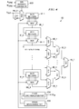
- FIG. 4 is a block diagram illustrating an example of the constitution of wobble clock reproduction part 63 in wobble reproduction part 6.
- Wobble clock reproduction part 63 reproduces the carrier component of wobble signal Sout output from pre-processor 61, and outputs the result as wobble clock signal CKw.
- Wobble clock reproduction part 63 shown as an example in FIG. 4 has sign inverter INV1, selector MU_0-MU_8, shift registers SF_1-SF_8, adders AD_1-AD_7, sign inversion controller 633, phase synchronization part 634, and period measurement part 635.
- the unit containing shift registers SF_1-SF_8 is an implementation of the delay signal generating means of the present invention.
- the unit containing adders AD_1-AD_7 is an implementation of the adder means of the present invention.
- Period measurement part 635 is an implementation of the period measurement means of the present invention.
- the unit containing selection part MU_0, sign inverter INV1, and sign inversion controller 633 is an implementation of the sign inversion means of the present invention.
- Sign inverter INV1 inverts the sign of wobble signal Sout output from pre-processor 61.
- Selection part MU_0 selects either wobble signal Sout or the output signal of sign inverter INV1 according to the control of sign inversion controller 633.
- sign inversion controller 633 predicts the phase change points (PC, PD) of the bit synchronization signal and the phase change points (PA, PB) of the word synchronization signal, and switches the selection of the signal in selection part MU_0 at the predicted phase change point.
- Shift register SF_i (i represents an integer of 1-8) has a circuit composed of plural flip-flops connected in series and holding the signal synchronized to the write clock signal of write clock generating part 9, and the wobble signal output from selection part MU_i-1 is input to the initial stage of said series-connected circuit.
- the wobble signal input to the initial stage of the series-connected circuit is sequentially shifted as it passes through the various stages.
- the number of stages in the series-connected circuit is selected such that the delay of the wobble signal output from the fmal stage with respect to the wobble signal input to the initial stage is longer than wobble period Tw.
- wobble period Tw is 32 times the period T of the write clock signal. Consequently, the number of stages in the series-connected circuit is set to at least 32. In this example, the number of stages in the series-connected circuit is 36.
- the hold signal is output to selection part MU_i.
- delay signals having 8 different delays are output from the 28 th to 36 th stages of the flip-flops to selection part MU_i.
- Selection part MU_i selects and outputs a delay signal corresponding to the measurement result of period measurement part 635 from the delay signals output from said 8 stages of the flip-flops of shift register SF_i.
- the output of adder AD_7 is the sum of all of the output signals from selection part MU_1-MU_8.
- Phase synchronization part 634 generates wobble clock signal CKw synchronously with the signal output from adder AD_7.
- Period measurement part 635 measures the period of the signal output from adder AD_7. Then, when a deviation in the measurement period takes place with respect to the delay time of the wobble signal propagating from the input of shift register SF_i to the output of selection part MU_i, by means of switching the selection of the signal in selection part MU_i, the delay time will be adjusted to correct for this deviation.
- the write operation in the optical disk of the present invention will be explained below as an operation of the data recording/reproduction device having the constitution shown in FIGS. 1-4 above.
- the laser beam for control signal generation is irradiated on optical disk 1, and the reflected light is converted by optical pickup 2 into an electronic signal.
- Analog front end part 3 performs A/D conversion, wave shaping, and other processes on the electronic signal to generate the tracking error signal, focusing error signal, wobble signal, and other control signals.
- servo-controller 13 controls the actuators of disk motor 16 and optical pickup 2, and guides the laser beam of optical pickup 2 to the target write position on optical disk 1.
- Pre-processor 61 of wobble demodulator 6 performs sampling rate conversion, offset removal, gain control, and other pretreatment processes on said wobble signal output from analog front end part 3, and the resulting signal is output as wobble signal Sout to wobble clock reproduction part 63 and demodulation processing part 62.
- Wobble signal Sout input to wobble clock reproduction part 63 performs sign inversion according to the control of sign inversion controller 633.
- sign inversion controller 633 predicts the phase change points (PA, PB, PC, PD) that can be generated in wobble signal Sout, and inverts the sign of wobble signal Sout at the predicted phase change point. For example, the sign of wobble signal Sout is inverted in the 2 wobble periods (bit synchronization signal) from phase change point PC to PD, and in the 4 wobble periods (word synchronization signal) from phase change point PA to PB.
- the wobble signal with a more uniform phase by means of said sign operation is then input to the series-connected 8-stage delay unit with each delay unit composed of shift register SF_i and selection part MCT_i. It then passes from the initial to the final stage of the delay units.
- the carrier components in the delay signals output from the delay units have the same phase. Consequently, in the signal output from adder AD_7 as a result of addition of the 8 delay signals, the amplitude of the carrier component is increased by about 8 times, and the out-phase noise component is attenuated.
- phase synchronization part 634 which generates wobble clock signal CKw locked to the phase of said signal.
- wobble clock signal CKw is produced, which is synchronized with the carrier component of the wobble signal.
- period measurement part 635 measures the period of the signal having the carrier component enhanced, and monitors deviation in the prediction period with respect to the propagation delay of each delay unit. When the deviation exceeds a prescribed range, by switching the selection of the signal in selection part MU_i, the delay of each delay unit is adjusted and the deviation is corrected.
- wobble signal Sout input to demodulation processing part 62 is integrated in adder 606 and flip-flop 607, and its integration value S2 is held in flip-flop 608 for each wobble period synchronously with said wobble clock signal CKw.
- Said integration value S2 is sequentially input to flip-flop 609 and subtractor 610, and the integration value of the first period of the two adjacent wobble periods is subtracted from the integration value of the second period to compute characteristic quantity S4 of the bit synchronization signal.
- peak value computation unit 611 the peak value and average value of said characteristic quantity S4 is calculated with an IIR filter, etc., and appropriate threshold S7 is set corresponding to the computed peak value and average value. For example, a prescribed coefficient is multiplied by the difference between the peak value and average value, and the obtained value is used to set threshold S7.
- first bit synchronization signal judgment part 614 compares characteristic quantity S4 with threshold S7, and on the basis of the result of the comparison, it is determined whether the signal of the signal range corresponding to the integration value of the computing element of characteristic quantity S4 is the bit synchronization signal.
- second bit synchronization signal judgment part 615 is based on the sign of the signal with respect to the signal determined to be the bit synchronization signal in first bit synchronization signal judgment part 614. That is, the signal in the signal range is determined to be the bit synchronization signal when a prescribed number of consecutive negative signals appear in the first period in the signal range of 2 wobble periods judged to be the bit synchronization signal (containing phase change point PC), and a prescribed number of consecutive positive signals appear in the second period (containing phase change point PD).
- first bit synchronization signal judgment part 614 and second bit synchronization signal judgment part 615 judge the bit synchronization signal, the final judgment is made that the signal of the signal range is the bit synchronization signal, and a "1," indicating the bit synchronization signal, is output from AND-gate 616.
- bit synchronization signal interpolator 617 interpolates the bit synchronization signal ("1" signal) in the output signal of AND-gate 616, and the result is output as bit synchronization signal Bsync of the demodulation result.
- the insertion point of the bit synchronization signal in wobble signal Sout is predicted, and when a "1" is not output from AND-gate 616 at the predicted insertion point, a "1" is interpolated at the predicted insertion point.
- bit synchronization signal interpolator 617 When the bit synchronization signal is not detected consecutively for a prescribed number of cycles at the predicted insertion point, bit synchronization signal interpolator 617 outputs a signal that indicates that the interpolation of the bit synchronization signal is invalid. As a result, a process for recovering synchronization between the actual bit synchronization signal and the detected bit synchronization signal is executed by a controller (not shown in the figure) of the data recording/reproduction device.
- bit synchronization signal Bsync when bit synchronization signal Bsync is demodulated, it is possible to predict the phase change points (PA, PB) of the word synchronization signal and the phase change points (PE, PF, PG, PH) of the bit signal obtained by insertion in the wobble signal on the basis of the timing.
- Flip-flops 618, 619 and subtractor 620 hold the integration values of predicted phase change points PA and PB from the integration values sequentially output from flip-flop 608 at timing of latch pulse LP2, and the integration value of phase change point PA is subtracted from the held integration value of said phase change point PB.
- characteristic quantity S10 of the word synchronization signal is calculated.
- first word synchronization signal judgment part 621 compares characteristic quantity S10 of the word synchronization signal and characteristic quantity S4 of the bit synchronization signal, and on the basis of the comparison result, determines whether the signal of the signal range corresponding to the integration value of the computing element of said signal S10 is the word synchronization signal.
- the determination of the word synchronization signal is performed on the basis of the result of comparison of the characteristic quantities of the bit synchronization signal and the word synchronization signal. Consequently, the judgment can be performed with greater precision than the judgment method that uses only the characteristic quantity of the word synchronization signal (for example, the judgment method based on the threshold as the characteristic quantity, etc.).
- second word synchronization signal judgment part 622 performs its judgment on the basis of the sign of the signal for the signal judged to be the word synchronization signal in said first word synchronization signal judgment part 621. That is, when a prescribed number of consecutive negative signals appear during the initial period (the period containing phase change point PA) of the signal range of 5 wobble periods judged to be the word synchronization signal, and a prescribed number of consecutive positive signals appear during the last period (the period containing phase change point PB), the signal in the signal range is judged to be the word synchronization signal.
- first word synchronization signal judgment part 621 and second word synchronization signal judgment part 622 judge the word synchronization signal, the final judgment is made that the signal of the signal range is the word synchronization signal, and a "1," indicating the word synchronization signal, is output from AND-gate 623.
- word synchronization signal interpolator 624 interpolates the word synchronization signal ("1" signal) in the output signal of AND-gate 623, and the result is output as word synchronization signal Wsync of the demodulation result.
- the insertion point of the word synchronization signal in wobble signal Sout is predicted, and when a "1" is not output from AND-gate 623 at the predicted insertion point, a "1" is interpolated at the predicted insertion point.
- word synchronization signal interpolator 624 When the word synchronization signal is not detected consecutively for a prescribed number of cycles at the predicted insertion point, word synchronization signal interpolator 624 outputs a signal that indicates that the interpolation of the word synchronization signal is invalid. As a result, a process for recovering the synchronization between the actual word synchronization signal and the detected word synchronization signal is executed by a controller (not shown in the figure) of the data recording/reproduction device.
- Flip-flops 625, 626 and subtractor 627 hold the integration values of predicted phase change points PG and PH from the integration values sequentially output from flip-flop 608 at the timing of latch pulse LP3, and the integration value of phase change point PG is subtracted from the held integration value of said phase change point PH. As a result, characteristic quantity S13 of the bit signal "1" is calculated.
- flip-flops 628, 629 and subtractor 630 hold the integration values of predicted phase change points PE and PF from the integration values sequentially output from flip-flop 608 at the timing of latch pulse LP4, and the integration value of phase change point PE is subtracted from the held integration value of said phase change point PF.
- characteristic quantity S16 of the bit signal of "0" is calculated.
- bit value judgment part 631 compares characteristic quantity S13 of the bit signal "1” and characteristic quantity S16 of the bit signal "0,” and, on the basis of the comparison result, determines whether the value of the bit signal inserted synchronously with the detected bit synchronization signal is "1" or "0.”
- the judgment of the bit value is performed on the basis of the result of comparison of the characteristic quantities of the bit signals "1" and "0.” Consequently, the judgment can be performed with greater precision than the judgment method that uses the characteristic quantity of only one (for example, the judgment method based on the threshold as the characteristic quantity, etc.).
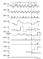
- FIG. 5 is a waveform diagram illustrating an example of the waveforms of the various portions of demodulation processing part 62 when the bit signal "0" is input.
- FIG. 5(A) shows wobble signal Sout
- FIG. 5(B) shows wobble clock signal CKw
- FIG. 5(C) shows latch pulse LP1
- FIG. 5(D) shows integration value S2
- FIG. 5(E) shows characteristic quantity S4 of the bit synchronization signal
- FIG. 5(G) shows latch pulse LP3
- FIG. 5(H) shows latch pulse LP4
- FIG. 5(I) shows the characteristic quantity S16 of the bit signal of "0”
- FIG. 5(J) shows characteristic quantity S13 of the bit signal of "1”
- FIG. 5(K) shows demodulated bit signal Bdat.
- FIG. 5(F) shows the difference value obtained by subtracting the integration value of the former period from the integration value of the latter period.
- This difference value is the maximum positive value with respect to the signal pattern of the bit signal having the phase change points separated from each other by 2 wobble periods (PE and PF, or PG and PH).
- wobble signal Sout contains the signal pattern of the bit synchronization signal characterized with two phase change points (PC, PD) separated from each other by 1 wobble period in periods T1 and T2. Consequently, characteristic feature S4 of the bit synchronization signal exceeds threshold S7 (FIG. 5(E)) in period T4 when the result of subtraction of the integration value of period T1 from the integration value of period T2 is output.
- threshold S7 FIG. 5(E)
- timing controller 632 outputs latch pulse LP3 at times t1 and t2 such that integration values S2 of periods T5 and T7 are held in flip-flops 626 and 625, respectively (FIG. 5(G)).
- timing controller 632 outputs latch pulse LP4 at times t2 and t3 so that integration values S2 of periods T7 and T9 are held in flip-flops 629 and 628, respectively (FIG. 5(H)).
- characteristic quantity S13 the difference between the integration values held in flip-flops 626 and 625 according to latch pulse LP3, and characteristic quantity S16, the difference between the integration values held in flip-flops 629 and 628 according to latch pulse LP4, are compared at time t3 when both values are determined, as shown in FIGS. 5(I) and (J), characteristic quantity S16 is larger than characteristic quantity S13. Consequently, bit value judgment part 631 determines that the value of the bit signal inserted synchronously with the bit synchronization signal in periods T1 and T2 is "0,” and bit signal Bdat of "0" is output (FIG. 5(K)).
- wobble demodulator 6 while wobble clock signal CKw is reproduced from the wobble signal output from analog front end part 3, bit synchronization signal Bsync, word synchronization signal Wsync and bit signal Bdat are demodulated.
- Write clock generating part 9 multiplies reproduced wobble clock signal CKw by a prescribed multiplier to generate the write clock signal. Also, wobble demodulator 7 performs the prescribed demodulation treatment for the demodulation signal of wobble demodulator 6, and the address information of optical disk 1 is reproduced.
- write data encoding part 8 performs the prescribed encoding processing for the write data supplied from a host device (not shown in the figure) and generates a write pulse row. Then, the write pulse row is output to write pulse generating part 10 at a timing corresponding to the address information reproduced by wobble demodulator 7.
- Write pulse generating part 10 performs the prescribed processing, which matches the characteristics of the disk as the object to be written to, for the input write pulse row to generate a write pulse signal, which is output to laser drive part 11.
- Laser drive part 11 drives the laser light source of optical pickup 2 corresponding to the write pulse signal to generate a laser beam for writing.
- the laser beam is irradiated corresponding to the write data supplied from the host device (not shown in the figure) at the target write site on optical disk 1, and a data write operation is carried out.
- the judgment of the bit value is performed on the basis of the result of comparison of the characteristic quantities of the bit signals "1' and "0.” Consequently, compared with the conventional method, in which the integration value of the wobble signal is compared with a fixed threshold, it is possible to reduce the risk of misjudging the bit value due to variations in the signal, etc., and it is possible to demodulate the bit signal with greater precision.
- characteristic quantity S4 of the bit synchronization signal is computed by performing prescribed sign operations on the integration values S2, respectively, during the periods where a phase change of the bit synchronization signal should take place in the signal range of the bit synchronization signal obtained by insertion in the wobble signal and finding the sum.
- the threshold for judging the bit synchronization signal can be set corresponding to the peak value and average value of the characteristic quantity of the bit synchronization signal computed as described above. Then, on the basis of comparison between the computed characteristic quantity of the bit synchronization signal and the set threshold, it is determined whether the signal of the signal range is a bit synchronization signal.
- the threshold for judging the bit synchronization signal is adjusted to track the bit synchronization signal and is kept at an appropriate value. Consequently, even when the amplitude of the wobble signal varies significantly, it is still possible to demodulate the bit synchronization signal with greater precision.
- output signal S10 of word synchronization signal is determined by the following operation: in the signal range of the word synchronization signal obtained by insertion in place of detected bit synchronization signal Bsync, prescribed sign operations are performed on integration values S2 in the periods where a phase change as word synchronization signal should take place, respectively, and the results are summed to obtain said characteristic quantity. On the basis of the comparison between said computed characteristic quantity S10 of the word synchronization signal and characteristic quantity S4 of the bit synchronization signal, it is determined whether the signal of the signal range is the word synchronization signal.
- the word synchronization signal is determined. Consequently, compared with the conventional method of comparing the integration value of the wobble signal and the fixed threshold, it is possible to reduce the risk of misjudging the bit value due to variations in the signal, etc., and it is possible to demodulate the word synchronization signal with greater precision.
- bit synchronization signal and word synchronization signal are determined for the periods in which a phase change takes place, and a final determination of the bit synchronization signal and word synchronization signal is made on the basis of whether a signal having a prescribed sign appears for a prescribed number of consecutive cycles.
- a delay signal made up of multiple delays corresponding to an integer multiple of the periods of the carrier component is added to the wobble signal. Consequently, even when a large amount of noise is superimposed on the wobble signal, it is still possible to attenuate the noise component, to extract the carrier component, and to reproduce wobble clock signal CKw synchronized to it.
- the present invention is not limited to the aforementioned embodiment, and various improvements can be performed.
- the aforementioned embodiment pertains to a type of data recording/reproduction device for optical disks.
- the present invention is not limited in this way. It may also be applied to data recording/reproduction devices using recording media other than optical disks (such as photomagnetic tapes, photomagnetic disks, etc.). Also, the present invention may also be applied to the data recorders with a data reproduction function.
- the demodulator of the present invention is used in the wobble demodulating part in the data recording/reproduction device of an optical disk.
- it may also be applied to communication devices, and various other devices and systems that demodulate phase modulated signals.
- 1 represents optical disk
- 2 represents optical pickup
- 3 represents analog front end part
- 4 represents clock reproduction part
- 5 represents read data decoder
- 6 represents wobble demodulator
- 7 represents wobble decoder
- 8 represents write data encoder
- 9 represents write clock generator
- 10 represents write pulse generator
- 12 represents interface part
- 13 represents servo-controller
- 14 represents actuator driver
- 15 represents rotary motor driver
- 16 represents disk motor
- 601 represents sampling rate converter
- 602 represents offset detector
- 603 represents offset removal part
- 604 represents gain controller
- 606 represents adder
- 610, 620, 627, 630 represent subtractors
- 607-609, 618, 619, 625, 626, 628, 629 represent flip-flops
- 611 represents peak value computation unit
- 612 represents average value computation unit
- 613 represents threshold setting part
- 614 represents first bit synchronization signal judgment part
- 615 represents second bit synchronization signal judgment part
- 621 represents first word synchronization
Landscapes
- Engineering & Computer Science (AREA)
- Signal Processing (AREA)
- Power Engineering (AREA)
- Manufacturing & Machinery (AREA)
- Chemical & Material Sciences (AREA)
- Chemical Kinetics & Catalysis (AREA)
- Electrochemistry (AREA)
- General Chemical & Material Sciences (AREA)
- Optical Recording Or Reproduction (AREA)
- Signal Processing For Digital Recording And Reproducing (AREA)
- Digital Transmission Methods That Use Modulated Carrier Waves (AREA)
- Charge And Discharge Circuits For Batteries Or The Like (AREA)
Applications Claiming Priority (2)
| Application Number | Priority Date | Filing Date | Title |
|---|---|---|---|
| JP2003317495 | 2003-09-09 | ||
| JP2003317495A JP3958269B2 (ja) | 2003-09-09 | 2003-09-09 | 復調装置およびこれを有するデータ記録装置 |
Publications (2)
| Publication Number | Publication Date |
|---|---|
| EP1515342A1 true EP1515342A1 (de) | 2005-03-16 |
| EP1515342B1 EP1515342B1 (de) | 2017-10-25 |
Family
ID=34131981
Family Applications (1)
| Application Number | Title | Priority Date | Filing Date |
|---|---|---|---|
| EP04104234.2A Expired - Lifetime EP1515342B1 (de) | 2003-09-09 | 2004-09-02 | Demodulator und datenwiedergabegerät |
Country Status (4)
| Country | Link |
|---|---|
| US (1) | US20050083797A1 (de) |
| EP (1) | EP1515342B1 (de) |
| JP (1) | JP3958269B2 (de) |
| KR (1) | KR20050026360A (de) |
Families Citing this family (32)
| Publication number | Priority date | Publication date | Assignee | Title |
|---|---|---|---|---|
| JP4142656B2 (ja) * | 2005-02-23 | 2008-09-03 | 富士通株式会社 | 光ディスクのwap復調方法及び復調装置 |
| KR100669434B1 (ko) | 2005-04-07 | 2007-01-15 | 삼성에스디아이 주식회사 | 이차 전지 모듈 제어방법 |
| KR100801852B1 (ko) * | 2005-04-21 | 2008-02-11 | 주식회사 엘지화학 | 배터리 팩 보호 장치 및 방법 |
| KR100717789B1 (ko) | 2005-07-29 | 2007-05-11 | 삼성에스디아이 주식회사 | 이차 전지 모듈의 전지 잔존용량 산출방법 |
| KR100740097B1 (ko) | 2005-10-20 | 2007-07-16 | 삼성에스디아이 주식회사 | 배터리의 soc 추정 방법 및 이를 이용한 배터리 관리시스템 |
| KR100739054B1 (ko) | 2005-10-20 | 2007-07-12 | 삼성에스디아이 주식회사 | 배터리 관리 시스템 및 배터리의 셀 전압 측정방법 |
| DE102006003834B4 (de) * | 2006-01-26 | 2012-02-16 | Infineon Technologies Ag | Vorrichtung und Verfahren zum Erfassen eines Frequenzversatzes |
| KR100825208B1 (ko) * | 2006-02-20 | 2008-04-25 | 주식회사 엘지화학 | 높은 효율성으로 작동되는 하이브리드형 전지팩 |
| JP2008010096A (ja) * | 2006-06-30 | 2008-01-17 | Toshiba Corp | 光ディスク装置および光ディスク判別方法 |
| CN1921366B (zh) * | 2006-09-25 | 2010-07-21 | 华为技术有限公司 | 一种编码符号对数似然比的实现方法和装置 |
| KR100796668B1 (ko) | 2006-09-26 | 2008-01-22 | 삼성에스디아이 주식회사 | 배터리 관리 시스템 및 그의 구동 방법 |
| KR100859688B1 (ko) | 2006-10-12 | 2008-09-23 | 삼성에스디아이 주식회사 | 배터리 관리 시스템 및 그의 구동 방법 |
| KR100814884B1 (ko) | 2006-10-16 | 2008-03-20 | 삼성에스디아이 주식회사 | 배터리 관리 시스템 및 그 구동방법 |
| KR100839381B1 (ko) | 2006-11-01 | 2008-06-20 | 삼성에스디아이 주식회사 | 배터리 관리 시스템 및 그 구동방법 |
| KR100882913B1 (ko) | 2007-03-19 | 2009-02-10 | 삼성에스디아이 주식회사 | 배터리 팩 |
| WO2009066908A2 (en) * | 2007-11-21 | 2009-05-28 | Dani Co., Ltd. | Portable charge/discharge apparatuses |
| JP5286809B2 (ja) * | 2008-02-05 | 2013-09-11 | ミツミ電機株式会社 | 半導体集積回路 |
| KR101081078B1 (ko) | 2008-11-14 | 2011-11-07 | 주식회사 엘지화학 | 센스 저항 파괴를 감지하여 배터리 팩을 보호하는 장치 및 방법 |
| KR100989061B1 (ko) * | 2009-04-20 | 2010-10-25 | 배트로닉스(주) | 군용 배터리팩 |
| US9159355B1 (en) * | 2010-01-21 | 2015-10-13 | Marvell International Ltd. | DVD-RAM header or land/groove detection |
| KR101312124B1 (ko) * | 2011-12-30 | 2013-09-26 | 넥스콘 테크놀러지 주식회사 | 배터리 관리 시스템의 단락 감지 장치 및 방법 |
| JP6530586B2 (ja) * | 2013-12-06 | 2019-06-12 | ミツミ電機株式会社 | 2次保護ic、2次保護icの制御方法、保護モジュール、及び電池パック |
| CN104810878B (zh) | 2014-01-28 | 2017-05-10 | 广东欧珀移动通信有限公司 | 过压过流保护电路和移动终端 |
| US10658852B2 (en) | 2017-01-05 | 2020-05-19 | Samsung Sdi Co., Ltd. | Battery pack and protection method of the battery pack |
| KR20180090145A (ko) | 2017-02-02 | 2018-08-10 | 삼성에스디아이 주식회사 | 배터리 팩, 배터리 관리 시스템 및 그 방법 |
| KR102232116B1 (ko) | 2017-06-13 | 2021-03-25 | 주식회사 엘지화학 | 밸런싱 저항을 이용한 과전압 방지 시스템 |
| WO2019173622A1 (en) | 2018-03-07 | 2019-09-12 | Anokiwave, Inc. | Phased array with low-latency control interface |
| US11205858B1 (en) | 2018-10-16 | 2021-12-21 | Anokiwave, Inc. | Element-level self-calculation of phased array vectors using direct calculation |
| US10985819B1 (en) * | 2018-10-16 | 2021-04-20 | Anokiwave, Inc. | Element-level self-calculation of phased array vectors using interpolation |
| KR102663798B1 (ko) | 2019-06-25 | 2024-05-03 | 주식회사 엘지에너지솔루션 | 배터리 시스템 |
| KR102652768B1 (ko) * | 2021-03-29 | 2024-04-01 | 엘에스일렉트릭(주) | 배터리 보호 장치 및 그 배터리 보호 장치의 제어 방법 |
| US20240291288A1 (en) * | 2021-07-17 | 2024-08-29 | Wright Energy Storage Technologies, Inc. | Automatic high-power electrical energy energy storage systems and management methods |
Citations (4)
| Publication number | Priority date | Publication date | Assignee | Title |
|---|---|---|---|---|
| US4453260A (en) * | 1982-06-15 | 1984-06-05 | Tokyo Shibaura Denki Kabushiki Kaisha | Synchronizing circuit for detecting and interpolating sync signals contained in digital signal |
| JP2001209937A (ja) * | 2000-01-27 | 2001-08-03 | Ricoh Co Ltd | 復調装置及び情報記録再生装置 |
| US6345018B1 (en) * | 1999-08-04 | 2002-02-05 | Ricoh Company, Ltd. | Demodulation circuit for demodulating wobbling signal |
| US6538982B1 (en) | 1999-01-25 | 2003-03-25 | Koninklijke Philips Electronics | Record carrier and apparatus for scanning the record carrier |
Family Cites Families (5)
| Publication number | Priority date | Publication date | Assignee | Title |
|---|---|---|---|---|
| JP3984426B2 (ja) * | 2001-03-13 | 2007-10-03 | パイオニア株式会社 | 情報再生装置、信号処理装置、情報再生方法および光学式記録媒体 |
| JP4121264B2 (ja) * | 2001-10-16 | 2008-07-23 | コーニンクレッカ フィリップス エレクトロニクス エヌ ヴィ | ディスクドライブ装置及びウォブル情報検出方法 |
| JP3566690B2 (ja) * | 2001-12-07 | 2004-09-15 | 株式会社リコー | ウォブル信号検出回路及び光ディスク装置 |
| JP2004318939A (ja) * | 2003-04-14 | 2004-11-11 | Victor Co Of Japan Ltd | 光記録媒体のウォブル情報検出方法及びウォブル情報検出装置 |
| TWI267827B (en) * | 2003-08-28 | 2006-12-01 | Mediatek Inc | Detector for detecting information carried by a signal having a sawtooth-like shape |
-
2003
- 2003-09-09 JP JP2003317495A patent/JP3958269B2/ja not_active Expired - Fee Related
-
2004
- 2004-09-02 EP EP04104234.2A patent/EP1515342B1/de not_active Expired - Lifetime
- 2004-09-08 KR KR1020040071815A patent/KR20050026360A/ko not_active Withdrawn
- 2004-09-09 US US10/938,257 patent/US20050083797A1/en not_active Abandoned
Patent Citations (4)
| Publication number | Priority date | Publication date | Assignee | Title |
|---|---|---|---|---|
| US4453260A (en) * | 1982-06-15 | 1984-06-05 | Tokyo Shibaura Denki Kabushiki Kaisha | Synchronizing circuit for detecting and interpolating sync signals contained in digital signal |
| US6538982B1 (en) | 1999-01-25 | 2003-03-25 | Koninklijke Philips Electronics | Record carrier and apparatus for scanning the record carrier |
| US6345018B1 (en) * | 1999-08-04 | 2002-02-05 | Ricoh Company, Ltd. | Demodulation circuit for demodulating wobbling signal |
| JP2001209937A (ja) * | 2000-01-27 | 2001-08-03 | Ricoh Co Ltd | 復調装置及び情報記録再生装置 |
Non-Patent Citations (2)
| Title |
|---|
| PATENT ABSTRACTS OF JAPAN vol. 2000, no. 25 12 April 2001 (2001-04-12) * |
| VLERKEN VAN J J L M ET AL: "Format detection for DVD+ReWritable 4.7 GB", INTERNATIONAL CONFERENCE ON CONSUMER ELECTRONICS. 2000 DIGEST OF TECHNICAL PAPERS. ICCE. JUNE 13-15, 2000, NEW YORK, NY : IEEE, US, 13 June 2000 (2000-06-13), pages 162 - 163, XP002197293, ISBN: 0-7803-6302-7 * |
Also Published As
| Publication number | Publication date |
|---|---|
| JP2005085392A (ja) | 2005-03-31 |
| KR20050026360A (ko) | 2005-03-15 |
| US20050083797A1 (en) | 2005-04-21 |
| JP3958269B2 (ja) | 2007-08-15 |
| EP1515342B1 (de) | 2017-10-25 |
Similar Documents
| Publication | Publication Date | Title |
|---|---|---|
| EP1515342B1 (de) | Demodulator und datenwiedergabegerät | |
| US5517476A (en) | Digital signal reproducing apparatus using a viterbi decoder | |
| JP3456592B2 (ja) | 光デイスク装置 | |
| JP3450922B2 (ja) | ディジタル信号再生装置 | |
| JPH06295540A (ja) | ディジタル信号検出回路 | |
| KR20030001520A (ko) | 어드레스 정보를 디스크 매체에 기록하는 방법 및 장치 | |
| US7852729B2 (en) | Optical disc apparatus with adjustable constraint length PRML | |
| WO2005024822A1 (ja) | 再生信号処理装置、及び再生信号処理方法 | |
| JP4053854B2 (ja) | 復調回路、光ディスク装置及び半導体集積回路 | |
| JP2001101807A (ja) | 光ディスク及び光ディスク再生装置 | |
| JP2004134009A (ja) | ウォブル復調装置および方法 | |
| CN101223600A (zh) | 数字信号再生装置 | |
| KR100960983B1 (ko) | 워블신호의 신호처리방법, 광디스크의 기록과 재생방법,광디스크장치, 프로그램, 및 기록매체 | |
| JP2004055079A (ja) | 記録媒体判別装置およびその方法 | |
| JP3927549B2 (ja) | トラッキング誤差検出装置 | |
| WO2006100981A1 (ja) | 情報記録媒体、情報再生装置、情報再生方法 | |
| CN101276632B (zh) | 解调电路及光盘装置 | |
| JP2942696B2 (ja) | 光ディスクからのデータ再生システム | |
| JP4186761B2 (ja) | 信号検出装置およびディスク装置 | |
| JP4545656B2 (ja) | アドレス復調回路及び光ディスク装置 | |
| JP2004178770A (ja) | 光ディスク装置 | |
| JP4343924B2 (ja) | トラッキング誤差検出装置 | |
| JPH0721615A (ja) | 光デイスク装置 | |
| JPH056619A (ja) | デジタルデータ記録および再生装置 | |
| JP2005339711A (ja) | 波形等化方法・情報再生方法・情報再生装置 |
Legal Events
| Date | Code | Title | Description |
|---|---|---|---|
| PUAI | Public reference made under article 153(3) epc to a published international application that has entered the european phase |
Free format text: ORIGINAL CODE: 0009012 |
|
| AK | Designated contracting states |
Kind code of ref document: A1 Designated state(s): AT BE BG CH CY CZ DE DK EE ES FI FR GB GR HU IE IT LI LU MC NL PL PT RO SE SI SK TR |
|
| AX | Request for extension of the european patent |
Extension state: AL HR LT LV MK |
|
| 17P | Request for examination filed |
Effective date: 20050916 |
|
| AKX | Designation fees paid |
Designated state(s): DE FR GB |
|
| REG | Reference to a national code |
Ref country code: DE Ref legal event code: R079 Ref document number: 602004051940 Country of ref document: DE Free format text: PREVIOUS MAIN CLASS: G11B0027240000 Ipc: G11B0020140000 |
|
| GRAP | Despatch of communication of intention to grant a patent |
Free format text: ORIGINAL CODE: EPIDOSNIGR1 |
|
| RIC1 | Information provided on ipc code assigned before grant |
Ipc: G11B 7/005 20060101ALI20170309BHEP Ipc: G11B 20/14 20060101AFI20170309BHEP Ipc: G11B 27/24 20060101ALI20170309BHEP Ipc: G11B 20/10 20060101ALI20170309BHEP |
|
| INTG | Intention to grant announced |
Effective date: 20170404 |
|
| GRAS | Grant fee paid |
Free format text: ORIGINAL CODE: EPIDOSNIGR3 |
|
| GRAJ | Information related to disapproval of communication of intention to grant by the applicant or resumption of examination proceedings by the epo deleted |
Free format text: ORIGINAL CODE: EPIDOSDIGR1 |
|
| GRAL | Information related to payment of fee for publishing/printing deleted |
Free format text: ORIGINAL CODE: EPIDOSDIGR3 |
|
| GRAR | Information related to intention to grant a patent recorded |
Free format text: ORIGINAL CODE: EPIDOSNIGR71 |
|
| GRAA | (expected) grant |
Free format text: ORIGINAL CODE: 0009210 |
|
| INTC | Intention to grant announced (deleted) | ||
| INTG | Intention to grant announced |
Effective date: 20170907 |
|
| AK | Designated contracting states |
Kind code of ref document: B1 Designated state(s): DE FR GB |
|
| REG | Reference to a national code |
Ref country code: GB Ref legal event code: FG4D |
|
| REG | Reference to a national code |
Ref country code: DE Ref legal event code: R096 Ref document number: 602004051940 Country of ref document: DE |
|
| REG | Reference to a national code |
Ref country code: DE Ref legal event code: R097 Ref document number: 602004051940 Country of ref document: DE |
|
| REG | Reference to a national code |
Ref country code: FR Ref legal event code: PLFP Year of fee payment: 15 |
|
| PLBE | No opposition filed within time limit |
Free format text: ORIGINAL CODE: 0009261 |
|
| STAA | Information on the status of an ep patent application or granted ep patent |
Free format text: STATUS: NO OPPOSITION FILED WITHIN TIME LIMIT |
|
| 26N | No opposition filed |
Effective date: 20180726 |
|
| PGFP | Annual fee paid to national office [announced via postgrant information from national office to epo] |
Ref country code: DE Payment date: 20190813 Year of fee payment: 16 Ref country code: FR Payment date: 20190819 Year of fee payment: 16 |
|
| PGFP | Annual fee paid to national office [announced via postgrant information from national office to epo] |
Ref country code: GB Payment date: 20190827 Year of fee payment: 16 |
|
| REG | Reference to a national code |
Ref country code: DE Ref legal event code: R119 Ref document number: 602004051940 Country of ref document: DE |
|
| GBPC | Gb: european patent ceased through non-payment of renewal fee |
Effective date: 20200902 |
|
| PG25 | Lapsed in a contracting state [announced via postgrant information from national office to epo] |
Ref country code: FR Free format text: LAPSE BECAUSE OF NON-PAYMENT OF DUE FEES Effective date: 20200930 Ref country code: DE Free format text: LAPSE BECAUSE OF NON-PAYMENT OF DUE FEES Effective date: 20210401 |
|
| PG25 | Lapsed in a contracting state [announced via postgrant information from national office to epo] |
Ref country code: GB Free format text: LAPSE BECAUSE OF NON-PAYMENT OF DUE FEES Effective date: 20200902 |