EP1511367B1 - Herstellung einer Leiterplatte - Google Patents
Herstellung einer Leiterplatte Download PDFInfo
- Publication number
- EP1511367B1 EP1511367B1 EP04254904A EP04254904A EP1511367B1 EP 1511367 B1 EP1511367 B1 EP 1511367B1 EP 04254904 A EP04254904 A EP 04254904A EP 04254904 A EP04254904 A EP 04254904A EP 1511367 B1 EP1511367 B1 EP 1511367B1
- Authority
- EP
- European Patent Office
- Prior art keywords
- metal
- substrate
- laser beam
- hole
- less portion
- Prior art date
- Legal status (The legal status is an assumption and is not a legal conclusion. Google has not performed a legal analysis and makes no representation as to the accuracy of the status listed.)
- Expired - Lifetime
Links
Images

Classifications
-
- H—ELECTRICITY
- H05—ELECTRIC TECHNIQUES NOT OTHERWISE PROVIDED FOR
- H05K—PRINTED CIRCUITS; CASINGS OR CONSTRUCTIONAL DETAILS OF ELECTRIC APPARATUS; MANUFACTURE OF ASSEMBLAGES OF ELECTRICAL COMPONENTS
- H05K3/00—Apparatus or processes for manufacturing printed circuits
- H05K3/22—Secondary treatment of printed circuits
-
- H—ELECTRICITY
- H05—ELECTRIC TECHNIQUES NOT OTHERWISE PROVIDED FOR
- H05K—PRINTED CIRCUITS; CASINGS OR CONSTRUCTIONAL DETAILS OF ELECTRIC APPARATUS; MANUFACTURE OF ASSEMBLAGES OF ELECTRICAL COMPONENTS
- H05K3/00—Apparatus or processes for manufacturing printed circuits
- H05K3/40—Forming printed elements for providing electric connections to or between printed circuits
- H05K3/42—Plated through-holes or plated via connections
- H05K3/423—Plated through-holes or plated via connections characterised by electroplating method
-
- H—ELECTRICITY
- H05—ELECTRIC TECHNIQUES NOT OTHERWISE PROVIDED FOR
- H05K—PRINTED CIRCUITS; CASINGS OR CONSTRUCTIONAL DETAILS OF ELECTRIC APPARATUS; MANUFACTURE OF ASSEMBLAGES OF ELECTRICAL COMPONENTS
- H05K3/00—Apparatus or processes for manufacturing printed circuits
- H05K3/46—Manufacturing multilayer circuits
-
- H—ELECTRICITY
- H05—ELECTRIC TECHNIQUES NOT OTHERWISE PROVIDED FOR
- H05K—PRINTED CIRCUITS; CASINGS OR CONSTRUCTIONAL DETAILS OF ELECTRIC APPARATUS; MANUFACTURE OF ASSEMBLAGES OF ELECTRICAL COMPONENTS
- H05K2201/00—Indexing scheme relating to printed circuits covered by H05K1/00
- H05K2201/09—Shape and layout
- H05K2201/09209—Shape and layout details of conductors
- H05K2201/095—Conductive through-holes or vias
- H05K2201/09536—Buried plated through-holes, i.e. plated through-holes formed in a core before lamination
-
- H—ELECTRICITY
- H05—ELECTRIC TECHNIQUES NOT OTHERWISE PROVIDED FOR
- H05K—PRINTED CIRCUITS; CASINGS OR CONSTRUCTIONAL DETAILS OF ELECTRIC APPARATUS; MANUFACTURE OF ASSEMBLAGES OF ELECTRICAL COMPONENTS
- H05K2201/00—Indexing scheme relating to printed circuits covered by H05K1/00
- H05K2201/09—Shape and layout
- H05K2201/09209—Shape and layout details of conductors
- H05K2201/095—Conductive through-holes or vias
- H05K2201/09563—Metal filled via
-
- H—ELECTRICITY
- H05—ELECTRIC TECHNIQUES NOT OTHERWISE PROVIDED FOR
- H05K—PRINTED CIRCUITS; CASINGS OR CONSTRUCTIONAL DETAILS OF ELECTRIC APPARATUS; MANUFACTURE OF ASSEMBLAGES OF ELECTRICAL COMPONENTS
- H05K2201/00—Indexing scheme relating to printed circuits covered by H05K1/00
- H05K2201/09—Shape and layout
- H05K2201/09209—Shape and layout details of conductors
- H05K2201/095—Conductive through-holes or vias
- H05K2201/096—Vertically aligned vias, holes or stacked vias
-
- H—ELECTRICITY
- H05—ELECTRIC TECHNIQUES NOT OTHERWISE PROVIDED FOR
- H05K—PRINTED CIRCUITS; CASINGS OR CONSTRUCTIONAL DETAILS OF ELECTRIC APPARATUS; MANUFACTURE OF ASSEMBLAGES OF ELECTRICAL COMPONENTS
- H05K2201/00—Indexing scheme relating to printed circuits covered by H05K1/00
- H05K2201/09—Shape and layout
- H05K2201/09209—Shape and layout details of conductors
- H05K2201/09654—Shape and layout details of conductors covering at least two types of conductors provided for in H05K2201/09218 - H05K2201/095
- H05K2201/09745—Recess in conductor, e.g. in pad or in metallic substrate
-
- H—ELECTRICITY
- H05—ELECTRIC TECHNIQUES NOT OTHERWISE PROVIDED FOR
- H05K—PRINTED CIRCUITS; CASINGS OR CONSTRUCTIONAL DETAILS OF ELECTRIC APPARATUS; MANUFACTURE OF ASSEMBLAGES OF ELECTRICAL COMPONENTS
- H05K2201/00—Indexing scheme relating to printed circuits covered by H05K1/00
- H05K2201/10—Details of components or other objects attached to or integrated in a printed circuit board
- H05K2201/10227—Other objects, e.g. metallic pieces
- H05K2201/1025—Metallic discs
-
- H—ELECTRICITY
- H05—ELECTRIC TECHNIQUES NOT OTHERWISE PROVIDED FOR
- H05K—PRINTED CIRCUITS; CASINGS OR CONSTRUCTIONAL DETAILS OF ELECTRIC APPARATUS; MANUFACTURE OF ASSEMBLAGES OF ELECTRICAL COMPONENTS
- H05K2203/00—Indexing scheme relating to apparatus or processes for manufacturing printed circuits covered by H05K3/00
- H05K2203/10—Using electric, magnetic and electromagnetic fields; Using laser light
- H05K2203/107—Using laser light
-
- H—ELECTRICITY
- H05—ELECTRIC TECHNIQUES NOT OTHERWISE PROVIDED FOR
- H05K—PRINTED CIRCUITS; CASINGS OR CONSTRUCTIONAL DETAILS OF ELECTRIC APPARATUS; MANUFACTURE OF ASSEMBLAGES OF ELECTRICAL COMPONENTS
- H05K2203/00—Indexing scheme relating to apparatus or processes for manufacturing printed circuits covered by H05K3/00
- H05K2203/12—Using specific substances
- H05K2203/128—Molten metals, e.g. casting thereof, or melting by heating and excluding molten solder
-
- H—ELECTRICITY
- H05—ELECTRIC TECHNIQUES NOT OTHERWISE PROVIDED FOR
- H05K—PRINTED CIRCUITS; CASINGS OR CONSTRUCTIONAL DETAILS OF ELECTRIC APPARATUS; MANUFACTURE OF ASSEMBLAGES OF ELECTRICAL COMPONENTS
- H05K3/00—Apparatus or processes for manufacturing printed circuits
- H05K3/10—Apparatus or processes for manufacturing printed circuits in which conductive material is applied to the insulating support in such a manner as to form the desired conductive pattern
- H05K3/102—Apparatus or processes for manufacturing printed circuits in which conductive material is applied to the insulating support in such a manner as to form the desired conductive pattern by bonding of conductive powder, i.e. metallic powder
-
- H—ELECTRICITY
- H05—ELECTRIC TECHNIQUES NOT OTHERWISE PROVIDED FOR
- H05K—PRINTED CIRCUITS; CASINGS OR CONSTRUCTIONAL DETAILS OF ELECTRIC APPARATUS; MANUFACTURE OF ASSEMBLAGES OF ELECTRICAL COMPONENTS
- H05K3/00—Apparatus or processes for manufacturing printed circuits
- H05K3/46—Manufacturing multilayer circuits
- H05K3/4602—Manufacturing multilayer circuits characterized by a special circuit board as base or central core whereon additional circuit layers are built or additional circuit boards are laminated
Definitions
- the present invention relates to a process for manufacturing a wiring board having a via and, more specifically, to a method for forming a via penetrating a substrate made of an insulation material while filling metal, by plating in a through-hole formed in the substrate, so that a plated metallic layer of a predetermined thickness is formed on the surface of the substrate.
- a multi-layer wiring substrate shown in Fig. 6 is used in an electronic part such as a semiconductor device.
- wiring patterns 102, 102, ... formed on opposite surfaces of a core substrate 100 of an insulation material such as a ceramic, a resin or others are electrically connected to wiring patterns 122, 122, ... formed in insulation layers 120, 120, ... made of an insulation material such as a resin or others by vias 104, 104, ... formed to penetrate the core substrate 100 and vias 124, 124, ... formed in the insulation layers 120, 120, ....
- a method for manufacturing such a core substrate 100 is disclosed, for example, in Japanese Unexamined Patent Publication (Kokai) No. 2002-16357 (paragraphs [0034] to [0047], Figs. 2 and 3 ).
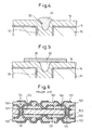
- a thick metallic layer 110 is formed on all surfaces of the core substrate 100, including an inner wall surface of a through-hole 106 bored in the core substrate 100 by a drill or others, by electrolytic plating in which a metallic layer 108 formed by electrolytic plating is used as a power supply layer (see Figs. 7(a) and 7(b) ).
- the through-hole 106 in which the metallic layers 108 and 110 are formed on the inner wall surface, is filled with resin 112, so that dome-like portions 112a are formed at opposite openings of the through-hole 106 (see Fig. 7(c) ). Then, the metallic layer 110 is subjected to the etching while using the dome-like portion 112a as a mask and is thinned to be a thin metallic layer 110a (see Fig. 7(d) ).
- the dome-like portion 112a is removed by the grinding or others so that an exposed surface of the resin 112 is flush with the surface of the thin metallic layer 110a (see Fig. 7(e) ), and thereafter, a metallic layer 114 is formed on the thin metallic layer 110a and the exposed surface of the resin layer 112 by the electroless plating, whereby the via 104 penetrating the core substrate 100 is obtained ( Fig. 7(f) ).
- the wiring patterns 102, 102, ... of a desired shape are formed by patterning a multi-metallic layer consisting of the metallic layer 108, the thin metallic layer 110a and the metallic layer 114 (see Fig. 7(g) ) to result in the core substrate 100 shown in Fig. 6 .
- the wiring patterns 102 are formed on opposite ends of the vias 104, 104, ... to facilitate the degree of freedom in the design of the wiring pattern 102.
- the via 104 of the core substrate 100 is formed of metal and resin, the electric properties thereof being largely different from each other, an improvement in electrical characteristics, such as impedance, is limited.
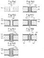
- a seed layer 204 of metal is formed on a surface of the substrate 200 including an inner wall surface of the through-hole 202 by electroless plating as shown in Fig. 8(b) .
- electrolytic plating is carried out while using the seed layer 204 as a power supply layer, to form a plated metallic layer 206 on the seed layer 204 as shown in Fig. 8(c) .
- the through-hole 202 is filled with metal to complete the via as shown in Fig. 8(d) , and the plated metallic layer 206 of a predetermined thickness is formed on the surface of the substrate 200.
- the plated metallic layer 206 is patterned to form a desired wiring pattern on each of the opposite surfaces of the substrate 200.
- a wiring substrate having the via, both of which ends are connected to the wiring patterns, is obtained.
- a void 208 may possibly be generated in the via or dimples 210 and 210 may possibly be formed in the plated metallic layer 206 at positions corresponding to the center of the openings of the through-hole 202.
- dimples 210 and 210 are smaller than a thickness of the plated metallic layers 206 formed on the respective surfaces of the substrate 200, it is possible to remove the dimples 210 and 210 by removing the plated metallic layer 206 by etching or other methods.
- the dimples 210 and 210 are not completely removable even if the plated metallic layer 206 is removed by etching or other methods.
- a number of vias must be formed, in general, in the core substrate 100, and it is extremely difficult to optimize the plating condition for all the through-holes 202 formed in the substrate 200. Accordingly, there may be some vias having the dimple 210 or the seam 212 among the plurality of vias formed in the substrate 200.
- a wiring pad having a diameter larger than that of the through-hole 202 is provided on each of the opposite end surfaces of the via to ensure the electric connection between the both.
- the provision of the wiring pad having the larger diameter on each of the opposite end surfaces of the respective via is problematic in that the degree of freedom is reduced in the design of wiring pattern formed in the substrate, and a high-density arrangement of the wiring pattern becomes difficult.
- JP 0 3050888 discloses the filling of a conductor via by meting a conductor ball with a laser beam.
- an object of the present invention is to provide a process for manufacturing a wiring board, having a via, particularly obtained by filling metal by plating in a through-hole formed in a substrate of insulation material, which via is non-problematic even if a wiring pattern is formed directly on the end surface therof.
- the inventor of the present invention has attained the object on the basis of an idea that, when the via is formed by filling metal by plating in the through-hole formed in the substrate made of an insulation material, it is effective to fill metal in a metal-less portion of a plated metallic layer corresponding to the opening of the through-hole, such as a dimple or a seam, in which no metal is filled.
- the inventor has become aware of that it is possible to fill the metal-less portion with molten metal obtained by emitting a YAG laser beam to a plurality of points in the plated metallic later in the vicinity of the peripheral edge of the opening having the metal-less portion, and has reached the present invention.
- a process for manufacturing a wiring board comprising a substrate made of an insulation material and having first and second surfaces, first and second conductor patters formed on the first and second surfaces, respectively, and a via conductor penetrating the substrate to electrically connect the first conductor pattern with the second conductor pattern; the process comprising the following steps of: forming the substrate with a through-hole penetrating thereto and defining openings at the first and second surfaces, respectively; plating the substrate with a metal so that a metal layer having a predetermined thickness is formed on the respective first and second surfaces of the substrate and the through-hole is substantially filled with the metal to be the via; irradiating a laser beam, as a plurality of spots, around a metal-vacant portion of the plated metal, such as a dimple or seam, at discontinuous positions corresponding to the openings of the through-hole such that the laser beam is not emitted at a point between successive ones of the discontinuous positions, so that a part of the plated
- a process for manufacturing a wiring board comprising a substrate made of an insulation material and having first and second surfaces, first and second conductor patterns formed on the first and second surfaces, respectively, and a via conductor penetrating the substrate to electrically connect the first conductor pattern with the second conductor pattern; the process comprising the following steps of: forming the substrate with a through-hole to penetrate the substrate from the first surface to the second surface; plating the substrate with a metal so that a metal layer having a predetermined thickness is formed on the respective first and second surfaces of the substrate and the through-hole is substantially filled with the metal to be the via; covering with a metal foil or metal powder a metal-less portion of the plated metal, such as a dimple or seam, at positions corresponding to the openings of the through-hole; irradiating a laser beam, as a plurality of spots, onto the metal foil or metal powder, at discontinuous positions such that the laser beam is not irradiated onto a point between successive ones
- the laser beam is sequentially emitted along the peripheral edge of the metal-less portion to melt part of the plated metal layer in the vicinity of the peripheral edge of the metal-less portion, which molten metal is filled in the metal-less portion such as a dimple or a seam, formed in the plated metallic layer corresponding to the opening of the through-hole.
- the metal-less portion once filled with the molten metal is molten again, whereby it is possible to homegenize the plated metallic layer corresponding to the opening of the through-hole.
- the metal-vacant portion such as a dimple or a seam
- the metal-less portion is formed in the plated metallic layer at a position corresponding to the opening of the through-hole formed in the substrate of insulation material, it is possible to fill the metal-less portion with molten metal which is part of the plated metal layer in the vicinity of the peripheral edge of the metal-less portion by the spot-like emission of the laser beam onto a plurality of points thereof.
- a through-hole 12 formed in a substrate 10 of insulation material such as resin is filled with metal such as copper by plating.
- the filling of the metal in the through-hole 12 by plating is carried out in the same manner as shown in Fig. 8 .
- a seed layer 14 consisting of metal such as copper is formed on the surface of the substrate 10 including the inner wall surface of the through-hole 12 formed in the substrate 10 of insulation material such as resin by electroless plating and, thereafter, a plated metallic layer 16 having a predetermined thickness is formed on the seed layer 14 while filling the through-hole 12, with metal such as copper, by the electrolytic plating wherein the seed layer 14 is used as a power supply layer.
- a dimple 20 which is a recess of a metal-less portion in the plated metallic layer 16 at a position in correspondence to the opening of the through-hole 12. This dimple 20 is deep and would be left on an end surface of a via even if the plated metallic layer 16 is removed by etching or other methods.
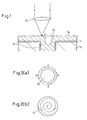
- a YAG laser beam focused by a lens 22 is emitted as a "spot" onto the plated metallic layer 16 forming the proximity of the peripheral edge of the dimple 20 to melt part of the plated metallic layer 16.
- the molten metal flows in the direction indicated by an arrow A to fill the dimple 20.
- the "spot-like” emission means a laser beam emission to be irradiated on to a very small area. Accordingly, it is necessary to repeat the "spot-like" emission of the YAG laser beam a plurality of times so that the dimple 20 is sufficiently filled with molten metal. At that time, if the "spot-like" emission of the YAG laser beam is repeated at the same point, this point is deeply excavated. To avoid such a trouble, the "spot-like" emission of the YAG laser beam is carried out to a plurality of different points in the vicinity of the peripheral edge of the dimple 20.
- the spot-like emission of the YAG laser beam is preferably carried out in the order of point a to point b, to point c, and to point d.
- the dimple 20 is filled with metal.
- a degree at which the dimple 20 is filled with metal is such that the dimple 20 is not necessarily completely filled with the metal but disappears after the plated metallic layer 16 has been removed by the etching or others.
- the spot-like emission of the YAG laser beam may be sequentially carried out along a spiral path, for example, shown in Fig. 2(b) , starting from the proximity of the peripheral edge of the opening of the through-hole 12 and going inward of the opening, whereby a portion of the dimple 20 which has been once filled with the metal is molten again to homogenize the plated metallic layer 16 in correspondence with the opening of the through-hole 12.
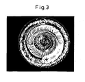
- Fig. 3 illustrates a state of the opening obtained by the spot-like emission of the YAG laser beam along the spiral path starting from the proximity of the peripheral edge of the opening of the through-hole 12 and going inward of the opening.
- a diameter of the opening of the through-hole 12 is 193 ⁇ m and the number of the spot-like emission of the YAG laser beam is 579 times.
- the plated metallic layer 16 is removed by the etching or others to result in the via, penetrating the substrate 10, having flat opposite end surfaces.
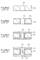
- the dimple 20 formed in the plated metallic layer 16 at a position corresponding to the opening of the through-hole 12 is covered with metallic powder 24 of the same kind as that forming the plated metallic layer 16.
- the YAG laser beam is spot-likely emitted to a plurality of positions of the metallic powder 24 to melt at least part of the metallic powder 24 and fill the same in the dimple 20.
- non-molten metallic powder 24 is removed if necessary, and the plated metallic layer 16 is removed by etching or other methods, whereby the via having a flat end surface is obtainable.
- the YAG laser beam is emitted onto a plurality of portions of the metallic foil 26 to melt at least part thereof and fill the dimple 20 with the molten metal.
- YAG laser beam has been used as a laser beam in the description with reference to Figs. 1 to 5
- an excimer laser beam may be used in place of the YAG laser beam, if it would be preferable to use a laser beam having a different wavelength.
- the emission of YAG laser is carried out automatically in accordance with a program regarding the design for the individual wiring board.
Landscapes
- Engineering & Computer Science (AREA)
- Manufacturing & Machinery (AREA)
- Microelectronics & Electronic Packaging (AREA)
- Printing Elements For Providing Electric Connections Between Printed Circuits (AREA)
- Production Of Multi-Layered Print Wiring Board (AREA)
- Manufacturing Of Printed Wiring (AREA)
Claims (6)
- Verfahren zum Herstellen einer Leiterplatte, aufweisend ein Substrat (10) aus einem Isolationsmaterial und aufweisend eine erste und eine zweite Oberfläche, ein erstes und ein zweites Leitermuster, die auf der ersten bzw. der zweiten Oberfläche ausgebildet sind, sowie eine Durchkontaktierung, die das Substrat durchdringt, um das erste Leitermuster mit dem zweiten Leitermuster elektrisch zu verbinden; wobei das Verfahren die folgenden Schritte aufweist:Bilden des Substrats (10), wobei ein Durchgangsloch (12) es durchdringt und Öffnungen an der ersten bzw. der zweiten Oberfläche definiert;Metallisieren des Substrats (10) mit einem Metall, so dass eine Metallschicht (16) mit einer vorbestimmten Dicke auf der jeweiligen ersten und zweiten Oberfläche des Substrats (10) ausgebildet wird und das Durchgangsloch (12) im Wesentlichen mit dem Metall, welches die Durchkontaktierung bilden wird, gefüllt wird;gekennzeichnet durch ein Emittieren eines Laserstrahls als eine Vielzahl von Punkten um einen metallfreien Bereich (20) des aufmetallisierten Metalls (16) herum, und zwar an nicht zusammenhängenden Positionen entsprechend einer der Öffnungen des Durchgangslochs (12), so dass der Laserstrahl an einem Punkt zwischen aufeinanderfolgenden der nicht zusammenhängenden Positionen nicht emittiert wird, so dass ein Teil des aufmetallisierten Metalls schmilzt, um den metallfreien Bereich (20) mit dem geschmolzenen Metall zu füllen.
- Verfahren nach Anspruch 1, bei dem der Laserstrahl periodisch entlang einer kreisförmigen Umfangskante einer Aussparung des metallfreien Bereichs eingestrahlt wird.
- Verfahren nach Anspruch 1, bei dem der Laserstrahl periodisch entlang eines spiralförmigen Pfads nach innen von einer Umfangskante einer Aussparung des metallfreien Bereichs aus eingestrahlt wird.
- Verfahren zum Herstellen einer Leiterplatte, aufweisend ein Substrat (10) aus einem Isolationsmaterial und aufweisend eine erste und eine zweite Oberfläche, ein erstes und ein zweites Leitermuster, die auf der ersten bzw. der zweiten Oberfläche ausgebildet sind, sowie eine Durchkontaktierung, die das Substrat (10) durchdringt, um das erste Leitermuster mit dem zweiten Leitermuster elektrisch zu verbinden; wobei das Verfahren die folgenden Schritte aufweist:Bilden des Substrats (10) mit einem Durchgangsloch (12), um das Substrat von der ersten Oberfläche zu der zweiten Oberfläche zu durchdringen;Metallisieren des Substrats mit einem Metall, so dass eine Metallschicht (16) mit einer vorbestimmten Dicke auf der jeweiligen ersten und zweiten Oberfläche des Substrats ausgebildet wird und das Durchgangsloch (12) im Wesentlichen mit dem Metall, welches die Durchkontaktierung bilden wird, gefüllt wird;Bedecken eines metallfreien Bereichs des aufmetallisierten Metalls (16), wie etwa einer Vertiefung (20) oder Fuge, mit einer Metallfolie oder einem Metallpulver (26; 24) an Positionen, die den Öffnungen des Durchgangslochs entsprechen;gekennzeichnet durch ein Einstrahlen eines Laserstrahls als eine Vielzahl von Punkten auf die Metallfolie (26) oder das Metallpulver (24) an nicht zusammenhängenden Positionen, so dass der Laserstrahl nicht an einem Punkt zwischen aufeinanderfolgenden der nicht zusammenhängenden Positionen eingestrahlt wird, so dass zumindest ein Teil der Metallfolie oder -pulvers schmilzt, um den metallfreien Bereich mit geschmolzenem Metall zu füllen.
- Verfahren nach Anspruch 4, bei dem der Laserstrahl periodisch entlang einer kreisförmigen Umfangskante des metallfreien Bereichs eingestrahlt wird.
- Verfahren nach Anspruch 4, bei dem der Laserstrahl periodisch entlang eines spiralförmigen Pfads nach innen von einer Umfangskante des metallfreien Bereichs aus eingestrahlt wird.
Applications Claiming Priority (2)
| Application Number | Priority Date | Filing Date | Title |
|---|---|---|---|
| JP2003299706 | 2003-08-25 | ||
| JP2003299706A JP4280583B2 (ja) | 2003-08-25 | 2003-08-25 | ヴィアの形成方法 |
Publications (3)
| Publication Number | Publication Date |
|---|---|
| EP1511367A2 EP1511367A2 (de) | 2005-03-02 |
| EP1511367A3 EP1511367A3 (de) | 2005-12-21 |
| EP1511367B1 true EP1511367B1 (de) | 2011-07-06 |
Family
ID=34101150
Family Applications (1)
| Application Number | Title | Priority Date | Filing Date |
|---|---|---|---|
| EP04254904A Expired - Lifetime EP1511367B1 (de) | 2003-08-25 | 2004-08-16 | Herstellung einer Leiterplatte |
Country Status (6)
| Country | Link |
|---|---|
| US (1) | US7205230B2 (de) |
| EP (1) | EP1511367B1 (de) |
| JP (1) | JP4280583B2 (de) |
| KR (1) | KR20050022324A (de) |
| CN (1) | CN100505989C (de) |
| TW (1) | TW200513159A (de) |
Families Citing this family (20)
| Publication number | Priority date | Publication date | Assignee | Title |
|---|---|---|---|---|
| JP4516320B2 (ja) * | 2004-01-08 | 2010-08-04 | シチズン電子株式会社 | Led基板 |
| US8308053B2 (en) | 2005-08-31 | 2012-11-13 | Micron Technology, Inc. | Microfeature workpieces having alloyed conductive structures, and associated methods |
| KR100753423B1 (ko) * | 2006-06-30 | 2007-08-30 | 주식회사 하이닉스반도체 | 비아패턴 형성방법 |
| KR100968977B1 (ko) * | 2008-10-17 | 2010-07-14 | 삼성전기주식회사 | 무수축 세라믹 기판 및 무수축 세라믹 기판의 제조 방법 |
| WO2011062037A1 (ja) * | 2009-11-20 | 2011-05-26 | イビデン株式会社 | プリント配線板及びプリント配線板の製造方法 |
| CN102215641B (zh) * | 2011-05-04 | 2012-11-07 | 深圳市博敏电子有限公司 | 一种带盘中孔的高密度印制板的加工工艺 |
| JP2015029027A (ja) * | 2013-07-31 | 2015-02-12 | イビデン株式会社 | プリント配線板 |
| US9053972B1 (en) | 2013-11-21 | 2015-06-09 | Freescale Semiconductor, Inc. | Pillar bump formed using spot-laser |
| US9474162B2 (en) | 2014-01-10 | 2016-10-18 | Freescale Semiocnductor, Inc. | Circuit substrate and method of manufacturing same |
| JP7009362B2 (ja) * | 2015-10-30 | 2022-01-25 | シューラット テクノロジーズ,インク. | 付加製造システム及び方法 |
| US10478311B2 (en) | 2017-08-14 | 2019-11-19 | Globus Medical, Inc. | Medical devices including titanium surface treatment |
| CN109673112B (zh) * | 2017-10-13 | 2021-08-20 | 鹏鼎控股(深圳)股份有限公司 | 柔性电路板以及柔性电路板的制作方法 |
| US10212828B1 (en) | 2017-11-27 | 2019-02-19 | International Business Machines Corporation | Via stub elimination by disrupting plating |
| JP7063095B2 (ja) * | 2018-05-07 | 2022-05-09 | 住友電気工業株式会社 | プリント配線板及びプリント配線板の製造方法 |
| US20190357364A1 (en) * | 2018-05-17 | 2019-11-21 | At&S Austria Technologie & Systemtechnik Aktiengesellschaft | Component Carrier With Only Partially Filled Thermal Through-Hole |
| KR102799625B1 (ko) | 2018-11-16 | 2025-04-23 | 삼성디스플레이 주식회사 | 표시 장치 및 이의 제조 방법 |
| CN110545620A (zh) * | 2019-08-06 | 2019-12-06 | 宁波华远电子科技有限公司 | 一种线路板通孔的填孔工艺 |
| WO2021049624A1 (ja) * | 2019-09-13 | 2021-03-18 | 株式会社ゼファー | 回路成型部品及び電子機器 |
| US12162074B2 (en) | 2020-11-25 | 2024-12-10 | Lawrence Livermore National Security, Llc | System and method for large-area pulsed laser melting of metallic powder in a laser powder bed fusion application |
| CN115484746A (zh) * | 2021-05-31 | 2022-12-16 | 宏启胜精密电子(秦皇岛)有限公司 | 电路板及其制造方法 |
Family Cites Families (13)
| Publication number | Priority date | Publication date | Assignee | Title |
|---|---|---|---|---|
| US4920070A (en) * | 1987-02-19 | 1990-04-24 | Fujitsu Limited | Method for forming wirings for a semiconductor device by filling very narrow via holes |
| US5110759A (en) * | 1988-12-20 | 1992-05-05 | Fujitsu Limited | Conductive plug forming method using laser planarization |
| JPH0350888A (ja) | 1989-07-19 | 1991-03-05 | Fujitsu Ltd | 導体ビアの修復方法 |
| US5380678A (en) * | 1991-03-12 | 1995-01-10 | Yu; Chang | Bilayer barrier metal method for obtaining 100% step-coverage in contact vias without junction degradation |
| US5340947A (en) | 1992-06-22 | 1994-08-23 | Cirqon Technologies Corporation | Ceramic substrates with highly conductive metal vias |
| US5454928A (en) | 1994-01-14 | 1995-10-03 | Watkins Johnson Company | Process for forming solid conductive vias in substrates |
| WO2001091924A1 (en) * | 2000-06-01 | 2001-12-06 | Board Of Regents, The University Of Texas System | Direct selective laser sintering of metals |
| JP2002016357A (ja) | 2000-06-30 | 2002-01-18 | Shinko Electric Ind Co Ltd | 多層配線基板の製造方法及び半導体装置 |
| JP4582938B2 (ja) | 2001-02-28 | 2010-11-17 | 京セラ株式会社 | 絶縁シートの製造方法および配線基板の製造方法 |
| JP2002270718A (ja) * | 2001-03-07 | 2002-09-20 | Seiko Epson Corp | 配線基板及びその製造方法、半導体装置及びその製造方法、回路基板並びに電子機器 |
| US6504111B2 (en) | 2001-05-29 | 2003-01-07 | International Business Machines Corporation | Solid via layer to layer interconnect |
| JP3807312B2 (ja) | 2002-01-18 | 2006-08-09 | 富士通株式会社 | プリント基板とその製造方法 |
| US6835657B2 (en) * | 2002-12-02 | 2004-12-28 | Applied Materials, Inc. | Method for recrystallizing metal in features of a semiconductor chip |
-
2003
- 2003-08-25 JP JP2003299706A patent/JP4280583B2/ja not_active Expired - Fee Related
-
2004
- 2004-08-10 US US10/914,227 patent/US7205230B2/en not_active Expired - Fee Related
- 2004-08-11 TW TW093124033A patent/TW200513159A/zh unknown
- 2004-08-16 EP EP04254904A patent/EP1511367B1/de not_active Expired - Lifetime
- 2004-08-20 KR KR1020040065730A patent/KR20050022324A/ko not_active Withdrawn
- 2004-08-24 CN CNB200410056988XA patent/CN100505989C/zh not_active Expired - Fee Related
Also Published As
| Publication number | Publication date |
|---|---|
| EP1511367A2 (de) | 2005-03-02 |
| TW200513159A (en) | 2005-04-01 |
| US7205230B2 (en) | 2007-04-17 |
| US20050048770A1 (en) | 2005-03-03 |
| EP1511367A3 (de) | 2005-12-21 |
| JP4280583B2 (ja) | 2009-06-17 |
| KR20050022324A (ko) | 2005-03-07 |
| CN100505989C (zh) | 2009-06-24 |
| CN1592553A (zh) | 2005-03-09 |
| JP2005072235A (ja) | 2005-03-17 |
Similar Documents
| Publication | Publication Date | Title |
|---|---|---|
| EP1511367B1 (de) | Herstellung einer Leiterplatte | |
| KR100682808B1 (ko) | 다층 회로 기판의 제조 방법 | |
| US7606038B2 (en) | Method for producing a printed circuit board with a heat radiating structure and a printed circuit board with a heat radiating structure | |
| KR100213857B1 (ko) | 반도체장치의 제조방법 및 반도체장치의 패키지 | |
| JPH10322027A (ja) | プリント配線板及びその製造方法 | |
| KR100751984B1 (ko) | 전자 부품의 제조 방법 및 전자 부품 | |
| JP2014232862A (ja) | 印刷回路基板 | |
| JP2004146836A (ja) | 回路基板及びその製造方法 | |
| US6730859B2 (en) | Substrate for mounting electronic parts thereon and method of manufacturing same | |
| JP2001053188A (ja) | 多層配線基板の製造方法 | |
| KR20050072678A (ko) | 다층 배선 기판 및 이의 제조 방법 | |
| JP2006100789A (ja) | 電気配線構造の製作方法 | |
| JP3838800B2 (ja) | 多層プリント配線板製造方法 | |
| US7935895B2 (en) | Structuring and circuitizing printed circuit board through-holes | |
| JP3583279B2 (ja) | 穴あけ加工方法 | |
| JP2000200975A (ja) | 多層配線基板の製造方法 | |
| EP1494516A2 (de) | Leiterplatte und Verfahren zu deren Herstellung | |
| US20060128143A1 (en) | Production method for electronic component and electronic component | |
| JP2002198653A (ja) | プリント配線板及びその製造方法 | |
| JP2000299563A (ja) | プリント配線板におけるビアホール形成方法 | |
| JPH11509991A (ja) | 恒久的接続のために電気回路の上に隆起した金属接点を作成する方法 | |
| JPH11154789A (ja) | 多層電子部品搭載用基板及びその製造方法 | |
| JP2020161730A (ja) | 配線基板 | |
| JP2004055633A (ja) | 配線基板の製造方法 |
Legal Events
| Date | Code | Title | Description |
|---|---|---|---|
| PUAI | Public reference made under article 153(3) epc to a published international application that has entered the european phase |
Free format text: ORIGINAL CODE: 0009012 |
|
| AK | Designated contracting states |
Kind code of ref document: A2 Designated state(s): AT BE BG CH CY CZ DE DK EE ES FI FR GB GR HU IE IT LI LU MC NL PL PT RO SE SI SK TR |
|
| AX | Request for extension of the european patent |
Extension state: AL HR LT LV MK |
|
| PUAL | Search report despatched |
Free format text: ORIGINAL CODE: 0009013 |
|
| AK | Designated contracting states |
Kind code of ref document: A3 Designated state(s): AT BE BG CH CY CZ DE DK EE ES FI FR GB GR HU IE IT LI LU MC NL PL PT RO SE SI SK TR |
|
| AX | Request for extension of the european patent |
Extension state: AL HR LT LV MK |
|
| 17P | Request for examination filed |
Effective date: 20060324 |
|
| AKX | Designation fees paid |
Designated state(s): DE FR GB |
|
| 17Q | First examination report despatched |
Effective date: 20100323 |
|
| GRAP | Despatch of communication of intention to grant a patent |
Free format text: ORIGINAL CODE: EPIDOSNIGR1 |
|
| GRAS | Grant fee paid |
Free format text: ORIGINAL CODE: EPIDOSNIGR3 |
|
| GRAA | (expected) grant |
Free format text: ORIGINAL CODE: 0009210 |
|
| AK | Designated contracting states |
Kind code of ref document: B1 Designated state(s): DE FR GB |
|
| REG | Reference to a national code |
Ref country code: GB Ref legal event code: FG4D |
|
| REG | Reference to a national code |
Ref country code: DE Ref legal event code: R096 Ref document number: 602004033352 Country of ref document: DE Effective date: 20110901 |
|
| PLBE | No opposition filed within time limit |
Free format text: ORIGINAL CODE: 0009261 |
|
| STAA | Information on the status of an ep patent application or granted ep patent |
Free format text: STATUS: NO OPPOSITION FILED WITHIN TIME LIMIT |
|
| 26N | No opposition filed |
Effective date: 20120411 |
|
| REG | Reference to a national code |
Ref country code: DE Ref legal event code: R097 Ref document number: 602004033352 Country of ref document: DE Effective date: 20120411 |
|
| PGFP | Annual fee paid to national office [announced via postgrant information from national office to epo] |
Ref country code: DE Payment date: 20130814 Year of fee payment: 10 |
|
| PGFP | Annual fee paid to national office [announced via postgrant information from national office to epo] |
Ref country code: GB Payment date: 20130814 Year of fee payment: 10 Ref country code: FR Payment date: 20130808 Year of fee payment: 10 |
|
| REG | Reference to a national code |
Ref country code: DE Ref legal event code: R119 Ref document number: 602004033352 Country of ref document: DE |
|
| GBPC | Gb: european patent ceased through non-payment of renewal fee |
Effective date: 20140816 |
|
| REG | Reference to a national code |
Ref country code: DE Ref legal event code: R119 Ref document number: 602004033352 Country of ref document: DE Effective date: 20150303 |
|
| REG | Reference to a national code |
Ref country code: FR Ref legal event code: ST Effective date: 20150430 |
|
| PG25 | Lapsed in a contracting state [announced via postgrant information from national office to epo] |
Ref country code: GB Free format text: LAPSE BECAUSE OF NON-PAYMENT OF DUE FEES Effective date: 20140816 Ref country code: DE Free format text: LAPSE BECAUSE OF NON-PAYMENT OF DUE FEES Effective date: 20150303 |
|
| PG25 | Lapsed in a contracting state [announced via postgrant information from national office to epo] |
Ref country code: FR Free format text: LAPSE BECAUSE OF NON-PAYMENT OF DUE FEES Effective date: 20140901 |