EP1511075B1 - Trägersubstrat für elektronisches Bauteil und dessen Herstellungsverfahren - Google Patents
Trägersubstrat für elektronisches Bauteil und dessen Herstellungsverfahren Download PDFInfo
- Publication number
- EP1511075B1 EP1511075B1 EP04020299.6A EP04020299A EP1511075B1 EP 1511075 B1 EP1511075 B1 EP 1511075B1 EP 04020299 A EP04020299 A EP 04020299A EP 1511075 B1 EP1511075 B1 EP 1511075B1
- Authority
- EP
- European Patent Office
- Prior art keywords
- electronic part
- metal
- ceramic substrate
- mounting substrate
- substrate
- Prior art date
- Legal status (The legal status is an assumption and is not a legal conclusion. Google has not performed a legal analysis and makes no representation as to the accuracy of the status listed.)
- Expired - Lifetime
Links
Images


Classifications
-
- H—ELECTRICITY
- H10—SEMICONDUCTOR DEVICES; ELECTRIC SOLID-STATE DEVICES NOT OTHERWISE PROVIDED FOR
- H10W—GENERIC PACKAGES, INTERCONNECTIONS, CONNECTORS OR OTHER CONSTRUCTIONAL DETAILS OF DEVICES COVERED BY CLASS H10
- H10W40/00—Arrangements for thermal protection or thermal control
- H10W40/20—Arrangements for cooling
- H10W40/25—Arrangements for cooling characterised by their materials
- H10W40/255—Arrangements for cooling characterised by their materials having a laminate or multilayered structure, e.g. direct bond copper [DBC] ceramic substrates
-
- H—ELECTRICITY
- H05—ELECTRIC TECHNIQUES NOT OTHERWISE PROVIDED FOR
- H05K—PRINTED CIRCUITS; CASINGS OR CONSTRUCTIONAL DETAILS OF ELECTRIC APPARATUS; MANUFACTURE OF ASSEMBLAGES OF ELECTRICAL COMPONENTS
- H05K3/00—Apparatus or processes for manufacturing printed circuits
- H05K3/10—Apparatus or processes for manufacturing printed circuits in which conductive material is applied to the insulating support in such a manner as to form the desired conductive pattern
- H05K3/101—Apparatus or processes for manufacturing printed circuits in which conductive material is applied to the insulating support in such a manner as to form the desired conductive pattern by casting or moulding of conductive material
-
- H—ELECTRICITY
- H10—SEMICONDUCTOR DEVICES; ELECTRIC SOLID-STATE DEVICES NOT OTHERWISE PROVIDED FOR
- H10W—GENERIC PACKAGES, INTERCONNECTIONS, CONNECTORS OR OTHER CONSTRUCTIONAL DETAILS OF DEVICES COVERED BY CLASS H10
- H10W70/00—Package substrates; Interposers; Redistribution layers [RDL]
- H10W70/01—Manufacture or treatment
- H10W70/02—Manufacture or treatment of conductive package substrates serving as an interconnection, e.g. of metal plates
-
- H—ELECTRICITY
- H10—SEMICONDUCTOR DEVICES; ELECTRIC SOLID-STATE DEVICES NOT OTHERWISE PROVIDED FOR
- H10W—GENERIC PACKAGES, INTERCONNECTIONS, CONNECTORS OR OTHER CONSTRUCTIONAL DETAILS OF DEVICES COVERED BY CLASS H10
- H10W90/00—Package configurations
-
- H—ELECTRICITY
- H05—ELECTRIC TECHNIQUES NOT OTHERWISE PROVIDED FOR
- H05K—PRINTED CIRCUITS; CASINGS OR CONSTRUCTIONAL DETAILS OF ELECTRIC APPARATUS; MANUFACTURE OF ASSEMBLAGES OF ELECTRICAL COMPONENTS
- H05K1/00—Printed circuits
- H05K1/02—Details
- H05K1/03—Use of materials for the substrate
- H05K1/0306—Inorganic insulating substrates, e.g. ceramic, glass
-
- H—ELECTRICITY
- H05—ELECTRIC TECHNIQUES NOT OTHERWISE PROVIDED FOR
- H05K—PRINTED CIRCUITS; CASINGS OR CONSTRUCTIONAL DETAILS OF ELECTRIC APPARATUS; MANUFACTURE OF ASSEMBLAGES OF ELECTRICAL COMPONENTS
- H05K1/00—Printed circuits
- H05K1/02—Details
- H05K1/03—Use of materials for the substrate
- H05K1/05—Insulated conductive substrates, e.g. insulated metal substrate
- H05K1/053—Insulated conductive substrates, e.g. insulated metal substrate the metal substrate being covered by an inorganic insulating layer
-
- H—ELECTRICITY
- H05—ELECTRIC TECHNIQUES NOT OTHERWISE PROVIDED FOR
- H05K—PRINTED CIRCUITS; CASINGS OR CONSTRUCTIONAL DETAILS OF ELECTRIC APPARATUS; MANUFACTURE OF ASSEMBLAGES OF ELECTRICAL COMPONENTS
- H05K2203/00—Indexing scheme relating to apparatus or processes for manufacturing printed circuits covered by H05K3/00
- H05K2203/12—Using specific substances
- H05K2203/128—Molten metals, e.g. casting thereof, or melting by heating and excluding molten solder
-
- H—ELECTRICITY
- H10—SEMICONDUCTOR DEVICES; ELECTRIC SOLID-STATE DEVICES NOT OTHERWISE PROVIDED FOR
- H10W—GENERIC PACKAGES, INTERCONNECTIONS, CONNECTORS OR OTHER CONSTRUCTIONAL DETAILS OF DEVICES COVERED BY CLASS H10
- H10W72/00—Interconnections or connectors in packages
- H10W72/071—Connecting or disconnecting
- H10W72/0711—Apparatus therefor
- H10W72/07178—Means for aligning
-
- H—ELECTRICITY
- H10—SEMICONDUCTOR DEVICES; ELECTRIC SOLID-STATE DEVICES NOT OTHERWISE PROVIDED FOR
- H10W—GENERIC PACKAGES, INTERCONNECTIONS, CONNECTORS OR OTHER CONSTRUCTIONAL DETAILS OF DEVICES COVERED BY CLASS H10
- H10W72/00—Interconnections or connectors in packages
- H10W72/071—Connecting or disconnecting
- H10W72/073—Connecting or disconnecting of die-attach connectors
- H10W72/07331—Connecting techniques
- H10W72/07336—Soldering or alloying
-
- H—ELECTRICITY
- H10—SEMICONDUCTOR DEVICES; ELECTRIC SOLID-STATE DEVICES NOT OTHERWISE PROVIDED FOR
- H10W—GENERIC PACKAGES, INTERCONNECTIONS, CONNECTORS OR OTHER CONSTRUCTIONAL DETAILS OF DEVICES COVERED BY CLASS H10
- H10W72/00—Interconnections or connectors in packages
- H10W72/50—Bond wires
- H10W72/531—Shapes of wire connectors
- H10W72/5363—Shapes of wire connectors the connected ends being wedge-shaped
-
- H—ELECTRICITY
- H10—SEMICONDUCTOR DEVICES; ELECTRIC SOLID-STATE DEVICES NOT OTHERWISE PROVIDED FOR
- H10W—GENERIC PACKAGES, INTERCONNECTIONS, CONNECTORS OR OTHER CONSTRUCTIONAL DETAILS OF DEVICES COVERED BY CLASS H10
- H10W72/00—Interconnections or connectors in packages
- H10W72/50—Bond wires
- H10W72/551—Materials of bond wires
- H10W72/552—Materials of bond wires comprising metals or metalloids, e.g. silver
- H10W72/5524—Materials of bond wires comprising metals or metalloids, e.g. silver comprising aluminium [Al]
-
- H—ELECTRICITY
- H10—SEMICONDUCTOR DEVICES; ELECTRIC SOLID-STATE DEVICES NOT OTHERWISE PROVIDED FOR
- H10W—GENERIC PACKAGES, INTERCONNECTIONS, CONNECTORS OR OTHER CONSTRUCTIONAL DETAILS OF DEVICES COVERED BY CLASS H10
- H10W90/00—Package configurations
- H10W90/701—Package configurations characterised by the relative positions of pads or connectors relative to package parts
- H10W90/731—Package configurations characterised by the relative positions of pads or connectors relative to package parts of die-attach connectors
- H10W90/734—Package configurations characterised by the relative positions of pads or connectors relative to package parts of die-attach connectors between a chip and a stacked insulating package substrate, interposer or RDL
-
- H—ELECTRICITY
- H10—SEMICONDUCTOR DEVICES; ELECTRIC SOLID-STATE DEVICES NOT OTHERWISE PROVIDED FOR
- H10W—GENERIC PACKAGES, INTERCONNECTIONS, CONNECTORS OR OTHER CONSTRUCTIONAL DETAILS OF DEVICES COVERED BY CLASS H10
- H10W90/00—Package configurations
- H10W90/701—Package configurations characterised by the relative positions of pads or connectors relative to package parts
- H10W90/751—Package configurations characterised by the relative positions of pads or connectors relative to package parts of bond wires
- H10W90/753—Package configurations characterised by the relative positions of pads or connectors relative to package parts of bond wires between laterally-adjacent chips
-
- H—ELECTRICITY
- H10—SEMICONDUCTOR DEVICES; ELECTRIC SOLID-STATE DEVICES NOT OTHERWISE PROVIDED FOR
- H10W—GENERIC PACKAGES, INTERCONNECTIONS, CONNECTORS OR OTHER CONSTRUCTIONAL DETAILS OF DEVICES COVERED BY CLASS H10
- H10W90/00—Package configurations
- H10W90/701—Package configurations characterised by the relative positions of pads or connectors relative to package parts
- H10W90/751—Package configurations characterised by the relative positions of pads or connectors relative to package parts of bond wires
- H10W90/754—Package configurations characterised by the relative positions of pads or connectors relative to package parts of bond wires between a chip and a stacked insulating package substrate, interposer or RDL
-
- H—ELECTRICITY
- H10—SEMICONDUCTOR DEVICES; ELECTRIC SOLID-STATE DEVICES NOT OTHERWISE PROVIDED FOR
- H10W—GENERIC PACKAGES, INTERCONNECTIONS, CONNECTORS OR OTHER CONSTRUCTIONAL DETAILS OF DEVICES COVERED BY CLASS H10
- H10W90/00—Package configurations
- H10W90/701—Package configurations characterised by the relative positions of pads or connectors relative to package parts
- H10W90/791—Package configurations characterised by the relative positions of pads or connectors relative to package parts of direct-bonded pads
- H10W90/794—Package configurations characterised by the relative positions of pads or connectors relative to package parts of direct-bonded pads between a chip and a stacked insulating package substrate, interposer or RDL
-
- Y—GENERAL TAGGING OF NEW TECHNOLOGICAL DEVELOPMENTS; GENERAL TAGGING OF CROSS-SECTIONAL TECHNOLOGIES SPANNING OVER SEVERAL SECTIONS OF THE IPC; TECHNICAL SUBJECTS COVERED BY FORMER USPC CROSS-REFERENCE ART COLLECTIONS [XRACs] AND DIGESTS
- Y10—TECHNICAL SUBJECTS COVERED BY FORMER USPC
- Y10T—TECHNICAL SUBJECTS COVERED BY FORMER US CLASSIFICATION
- Y10T29/00—Metal working
- Y10T29/49—Method of mechanical manufacture
- Y10T29/49002—Electrical device making
- Y10T29/49117—Conductor or circuit manufacturing
- Y10T29/49124—On flat or curved insulated base, e.g., printed circuit, etc.
- Y10T29/49126—Assembling bases
-
- Y—GENERAL TAGGING OF NEW TECHNOLOGICAL DEVELOPMENTS; GENERAL TAGGING OF CROSS-SECTIONAL TECHNOLOGIES SPANNING OVER SEVERAL SECTIONS OF THE IPC; TECHNICAL SUBJECTS COVERED BY FORMER USPC CROSS-REFERENCE ART COLLECTIONS [XRACs] AND DIGESTS
- Y10—TECHNICAL SUBJECTS COVERED BY FORMER USPC
- Y10T—TECHNICAL SUBJECTS COVERED BY FORMER US CLASSIFICATION
- Y10T29/00—Metal working
- Y10T29/49—Method of mechanical manufacture
- Y10T29/49002—Electrical device making
- Y10T29/49117—Conductor or circuit manufacturing
- Y10T29/49124—On flat or curved insulated base, e.g., printed circuit, etc.
- Y10T29/4913—Assembling to base an electrical component, e.g., capacitor, etc.
- Y10T29/49146—Assembling to base an electrical component, e.g., capacitor, etc. with encapsulating, e.g., potting, etc.
-
- Y—GENERAL TAGGING OF NEW TECHNOLOGICAL DEVELOPMENTS; GENERAL TAGGING OF CROSS-SECTIONAL TECHNOLOGIES SPANNING OVER SEVERAL SECTIONS OF THE IPC; TECHNICAL SUBJECTS COVERED BY FORMER USPC CROSS-REFERENCE ART COLLECTIONS [XRACs] AND DIGESTS
- Y10—TECHNICAL SUBJECTS COVERED BY FORMER USPC
- Y10T—TECHNICAL SUBJECTS COVERED BY FORMER US CLASSIFICATION
- Y10T29/00—Metal working
- Y10T29/49—Method of mechanical manufacture
- Y10T29/49002—Electrical device making
- Y10T29/49117—Conductor or circuit manufacturing
- Y10T29/49124—On flat or curved insulated base, e.g., printed circuit, etc.
- Y10T29/49155—Manufacturing circuit on or in base
Definitions
- EP 0 676 800 A2 relates to a metal/ ceramic bonding (MBC) substrate comprising a ceramic substrate, heat-dissipating fins bonded to one side of said ceramic substrate; a metal plate, one side of which is bonded to the other side of said ceramic substrate and further disclosing that MBC components can be used as substrates for mounting large-power electronic elements.
- MBC metal/ ceramic bonding
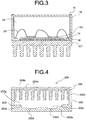
- the electronic parts 16 By thus bonding the electronic parts 16 directly to the circuit forming metal plate 14 of aluminum or an aluminum alloy without using any solders, it is possible to enhance thermal conductivity to improve heat sink characteristics. In addition, it is difficult to produce voids which are easily produced when a solder is used, and the thermal conductivity of aluminum or an aluminum alloy is higher than that of solders, so that it is possible to improve heat sink characteristics and reliability. In addition, it is not required to use any high-temperature solders which are difficult to be lead-free solders, so that the electronic part mounting substrate can be lead-free. Moreover, it is not required to plate the circuit forming metal plate 14 in order to improve solder wettability. Furthermore, the electronic parts 16 may be any electronic parts, such as semiconductor chips, resistor chips and capacitor chips, unless they are reacted with a molten metal to produce any alloys or compounds.
- the bonding interface between the SiC chip 508 and the aluminum circuit plate 506, the bonding interface between the aluminum circuit plate 506 and the ceramic substrate 504, and the bonding interface between the ceramic substrate 504 and the aluminum base plate 502 were examined by an ultrasonic detector. Then, no bonding failure was detected, and no crack was observed on the ceramic substrate 504.
Landscapes
- Engineering & Computer Science (AREA)
- Manufacturing & Machinery (AREA)
- Microelectronics & Electronic Packaging (AREA)
- Cooling Or The Like Of Semiconductors Or Solid State Devices (AREA)
- Structure Of Printed Boards (AREA)
Claims (12)
- Verfahren zum Erzeugen eines Trägersubstrats mit einem elektronischen Bauteil, bei dem ein Metallelement (12, 121, 302, 402, 502) an eine Seite eines Keramiksubstrats (10, 304, 404, 504) gebonded wird und eine Seite einer Metallscheibe (14, 306, 406, 506) an die andere Seite des Keramiksubstrats (10, 304, 404, 504) gebonded wird, wobei ein elektronisches Bauteil (16, 161, 308, 408, 508) an die andere Seite der Metallscheibe (14, 306, 406, 506) montiert wird, wobei das Verfahren die Schritte umfasst, dass:ein Keramiksubstrat (10, 304, 404, 504) und ein elektronisches Bauteil (16, 161, 308, 408, 508) in einer Form (100, 200, 400, 500) so angeordnet werden, dass das Keramiksubstrat (10, 304, 404, 504) von dem elektronischen Bauteil (16, 161, 308, 408, 508) beabstandet ist;geschmolzenes Metall in die Form (100, 200, 400, 500) so injiziert wird, dass das geschmolzene Metall beide Seiten des Keramiksubstrats (10, 304, 404, 504) und das elektronische Bauteil (16, 161, 308, 408, 508) kontaktiert;die Form (100, 200, 400, 500) gekühlt wird, um das geschmolzene Metall erstarren zu lassen, um ein Metallelement (12, 121, 302, 402, 502) an einer Seite des Keramiksubstrats (10, 304, 404, 504) so auszubilden, dass das Metallelement (12, 121, 302, 402, 502) direkt an die eine Seite des Keramiksubstrats (10, 304, 404, 504) gebonded ist, und um eine Metallscheibe (14, 306, 406, 506) an der anderen Seite des Keramiksubstrats (10, 304, 404, 504) so auszubilden, dass eine Seite der Metallscheibe (14, 306, 406, 506) direkt an die andere Seite des Keramiksubstrats (10, 304, 404, 504) gebonded ist; unddas elektronische Bauteil (16, 161, 308, 408, 508) direkt an die andere Seite der Metallscheibe (14, 306, 406, 506) gebonded wird, wenn die Metallscheibe (14, 306, 406, 506) ausgebildet wird.
- Verfahren zum Erzeugen eines Trägersubstrats mit einem elektronischen Bauteil nach Anspruch 1,
wobei das elektronische Bauteil (16, 161, 308, 408, 508) aus einem Material besteht, welches mit dem geschmolzenen Metall keinerlei Legierungen oder Verbindungen erzeugt. - Verfahren zum Erzeugen eines Trägersubstrats mit einem elektronischen Bauteil nach Anspruch 1,
wobei das elektronische Bauteil (16, 161, 308, 408, 508) ein Halbleiterchip (161, 308, 408, 508), ein Widerstandschip oder ein Kondensatorchip ist. - Verfahren zum Erzeugen eines Trägersubstrats mit einem elektronischen Bauteil nach Anspruch 1,
wobei das elektronische Bauteil (16, 161, 308, 408, 508) ein SiC-Chip (308, 408, 508) ist. - Verfahren zum Erzeugen eines Trägersubstrats mit einem elektronischen Bauteil nach Anspruch 1,
wobei das geschmolzene Metall geschmolzenes Aluminium oder eine geschmolzene Aluminiumlegierung ist. - Verfahren zum Erzeugen eines Leistungsmoduls, das die Schritte umfasst, dass:ein Gehäuse (18), das Elektroden (19) aufweist, an einem Trägersubstrat mit einem elektronischen Bauteil montiert wird, welches durch ein Verfahren zum Erzeugen eines Trägersubstrats mit einem elektronischen Bauteil nach Anspruch 1 erzeugt wird, und wobei das elektronische Bauteil (16, 161, 308, 408, 508) ein Halbleiterchip (161, 308, 408, 508) ist;die Elektroden (19) des Gehäuses (18) mit dem Halbleiterchip (161, 308, 408, 508) verbunden werden; undein Isoliermaterial in das Gehäuse (18) eingefüllt wird.
- Verfahren zum Erzeugen eines Trägersubstrats mit einem elektronischen Bauteil nach Anspruch 1, welches ferner die Schritte umfasst, dass:ein Bonding-Substrat, bei dem das Keramiksubstrat (10, 304, 404, 504), das Metallelement (12, 121, 302, 402, 502), die Metallscheibe (14, 306, 406, 506) und das elektronische Bauteil (16, 161, 308, 408, 508) miteinander zusammengebaut sind, aus der Form (100, 200, 400, 500) entnommen wird; unddanach ein Ätz-Abdecklack auf einer Oberfläche der Metallscheibe (14, 306, 406, 506) ausgebildet wird, um durch Ätzen eine Schaltung auf der Metallscheibe (14, 306, 406, 506) auszubilden.
- Verfahren zum Erzeugen eines Trägersubstrats mit einem elektronischen Bauteil nach Anspruch 7, wobei das Ätzen ausgeführt wird, nachdem die Metallscheibe (14, 306, 406, 506) maschinell bearbeitet wurde.
- Trägersubstrat mit einem elektronischen Bauteil, das durch das Verfahren nach Anspruch 1 erhalten wurde, wobei das Trägersubstrat mit einem elektronischen Bauteil umfasst:ein Keramiksubstrat (10, 304, 404, 504);ein Metallelement (12, 121, 302, 402, 502), das an eine Seite des Keramiksubstrats (10, 304, 404, 504) gebonded ist;eine Metallscheibe (14, 306, 406, 506), deren eine Seite direkt an die andere Seite des Keramiksubstrats (10, 304, 404, 504) gebondet ist; undein elektronisches Bauteil (16, 161, 308, 408, 508), das direkt an die andere Seite der Metallscheibe (14, 306, 406, 506) gebondet ist, wobei das elektronische Bauteil (16, 161, 308, 408, 508) ein Halbleiterchip (161, 308, 408, 508) ist.
- Trägersubstrat mit einem elektronischen Bauteil nach Anspruch 9, wobei der Halbleiterchip (16, 161, 308, 408, 508) ein SiC-Chip (308, 408, 508) ist.
- Trägersubstrat mit einem elektronischen Bauteil nach Anspruch 9, wobei das Metallelement (12, 121, 302, 402, 502) und die Metallscheibe (14, 306, 406, 506) aus Aluminium oder einer Aluminiumlegierung bestehen.
- Leistungsmodul, umfassend:ein Trägersubstrat mit einem elektronischen Bauteil nach Anspruch 9;ein Gehäuse (18) mit Elektroden (19), wobei das Gehäuse (18) an dem Trägersubstrat mit einem elektronischen Bauteil montiert ist, wobei die Elektroden (19) des Gehäuses (18) mit dem Halbleiterchip (161, 308, 408, 508) verbunden sind; undein Isoliermaterial, das in das Gehäuse (18) eingefüllt ist.
Applications Claiming Priority (2)
| Application Number | Priority Date | Filing Date | Title |
|---|---|---|---|
| JP2003209111 | 2003-08-27 | ||
| JP2003209111A JP4028452B2 (ja) | 2003-08-27 | 2003-08-27 | 電子部品搭載基板およびその製造方法 |
Publications (3)
| Publication Number | Publication Date |
|---|---|
| EP1511075A2 EP1511075A2 (de) | 2005-03-02 |
| EP1511075A3 EP1511075A3 (de) | 2008-06-04 |
| EP1511075B1 true EP1511075B1 (de) | 2018-10-10 |
Family
ID=34100730
Family Applications (1)
| Application Number | Title | Priority Date | Filing Date |
|---|---|---|---|
| EP04020299.6A Expired - Lifetime EP1511075B1 (de) | 2003-08-27 | 2004-08-26 | Trägersubstrat für elektronisches Bauteil und dessen Herstellungsverfahren |
Country Status (3)
| Country | Link |
|---|---|
| US (2) | US7159310B2 (de) |
| EP (1) | EP1511075B1 (de) |
| JP (1) | JP4028452B2 (de) |
Families Citing this family (22)
| Publication number | Priority date | Publication date | Assignee | Title |
|---|---|---|---|---|
| JP4441671B2 (ja) * | 2003-09-22 | 2010-03-31 | Dowaメタルテック株式会社 | 金属−セラミックス接合回路基板の製造方法 |
| JP4543279B2 (ja) * | 2004-03-31 | 2010-09-15 | Dowaメタルテック株式会社 | アルミニウム接合部材の製造方法 |
| JP2006121046A (ja) * | 2004-09-24 | 2006-05-11 | Meiko:Kk | 回路基板 |
| JP5176042B2 (ja) * | 2004-11-05 | 2013-04-03 | Dowaメタルテック株式会社 | 電子部品搭載基板の製造装置および製造方法 |
| DE102005001148B3 (de) * | 2005-01-10 | 2006-05-18 | Siemens Ag | Elektronikeinheit mit EMV-Schirmung |
| JP4585416B2 (ja) * | 2005-09-22 | 2010-11-24 | 富士通株式会社 | 基板の反り低減構造および基板の反り低減方法 |
| JP4711792B2 (ja) * | 2005-09-26 | 2011-06-29 | 三洋電機株式会社 | 回路装置 |
| EP2006895B1 (de) * | 2006-03-08 | 2019-09-18 | Kabushiki Kaisha Toshiba | Elektronisches komponentenmodul |
| JP2007294891A (ja) * | 2006-03-30 | 2007-11-08 | Dowa Metaltech Kk | 放熱器 |
| JP2007305962A (ja) * | 2006-05-12 | 2007-11-22 | Honda Motor Co Ltd | パワー半導体モジュール |
| JP4797077B2 (ja) * | 2009-02-18 | 2011-10-19 | 株式会社日立製作所 | 半導体パワーモジュール、電力変換装置、および、半導体パワーモジュールの製造方法 |
| US8520389B2 (en) | 2009-12-02 | 2013-08-27 | Hamilton Sundstrand Corporation | Power semiconductor module for wide temperature applications |
| CN102742008B (zh) * | 2010-02-05 | 2015-07-01 | 三菱综合材料株式会社 | 功率模块用基板及功率模块 |
| JP5565147B2 (ja) * | 2010-06-30 | 2014-08-06 | 株式会社デンソー | 半導体モジュールの製造方法 |
| JP2013123014A (ja) * | 2011-12-12 | 2013-06-20 | Toyota Industries Corp | 半導体装置 |
| JP6012990B2 (ja) * | 2012-03-19 | 2016-10-25 | 日本軽金属株式会社 | 放熱器一体型基板の製造方法 |
| JP5631446B2 (ja) * | 2013-06-13 | 2014-11-26 | Dowaメタルテック株式会社 | 金属−セラミックス接合基板の製造方法 |
| JP6139329B2 (ja) * | 2013-08-16 | 2017-05-31 | 日本碍子株式会社 | セラミック回路基板及び電子デバイス |
| JP6799392B2 (ja) * | 2016-06-20 | 2020-12-16 | Dowaメタルテック株式会社 | 金属−セラミックス接合基板およびその製造方法 |
| JP7127641B2 (ja) * | 2017-05-11 | 2022-08-30 | 住友電気工業株式会社 | 半導体装置 |
| CN112563224A (zh) * | 2020-12-04 | 2021-03-26 | 合肥圣达电子科技实业有限公司 | 一种用于大功率半导体芯片散热的微通道装置 |
| US20220399244A1 (en) * | 2021-06-10 | 2022-12-15 | Amulaire Thermal Technology, Inc. | Thermally conductive and electrically insulating substrate |
Citations (1)
| Publication number | Priority date | Publication date | Assignee | Title |
|---|---|---|---|---|
| US20030063442A1 (en) * | 2000-05-16 | 2003-04-03 | Mitsubishi Denki Kabushiki Kaisha | Power module |
Family Cites Families (10)
| Publication number | Priority date | Publication date | Assignee | Title |
|---|---|---|---|---|
| US4459607A (en) * | 1981-06-18 | 1984-07-10 | Burroughs Corporation | Tape automated wire bonded integrated circuit chip assembly |
| US4700273A (en) * | 1986-06-03 | 1987-10-13 | Kaufman Lance R | Circuit assembly with semiconductor expansion matched thermal path |
| KR0173782B1 (ko) * | 1989-10-09 | 1999-02-01 | 나가노 다께시 | 전기 또는 전자회로의 성형에 사용되는 세라믹기판 |
| US5381304A (en) * | 1993-06-11 | 1995-01-10 | Honeywell Inc. | Reworkable encapsulated electronic assembly and method of making same |
| JP2918191B2 (ja) * | 1994-04-11 | 1999-07-12 | 同和鉱業株式会社 | 金属−セラミックス複合部材の製造方法 |
| AT404083B (de) * | 1995-04-18 | 1998-08-25 | Electrovac | Verfahren zum herstellen von gehäusen |
| JP3901427B2 (ja) * | 1999-05-27 | 2007-04-04 | 松下電器産業株式会社 | 電子装置とその製造方法およびその製造装置 |
| JP4649027B2 (ja) * | 1999-09-28 | 2011-03-09 | 株式会社東芝 | セラミックス回路基板 |
| JP4756200B2 (ja) | 2000-09-04 | 2011-08-24 | Dowaメタルテック株式会社 | 金属セラミックス回路基板 |
| CN1184684C (zh) * | 2000-10-05 | 2005-01-12 | 三洋电机株式会社 | 半导体装置和半导体模块 |
-
2003
- 2003-08-27 JP JP2003209111A patent/JP4028452B2/ja not_active Expired - Fee Related
-
2004
- 2004-08-24 US US10/925,640 patent/US7159310B2/en not_active Expired - Fee Related
- 2004-08-26 EP EP04020299.6A patent/EP1511075B1/de not_active Expired - Lifetime
-
2006
- 2006-11-29 US US11/605,723 patent/US8039757B2/en not_active Expired - Fee Related
Patent Citations (1)
| Publication number | Priority date | Publication date | Assignee | Title |
|---|---|---|---|---|
| US20030063442A1 (en) * | 2000-05-16 | 2003-04-03 | Mitsubishi Denki Kabushiki Kaisha | Power module |
Also Published As
| Publication number | Publication date |
|---|---|
| US20070089291A1 (en) | 2007-04-26 |
| EP1511075A2 (de) | 2005-03-02 |
| JP4028452B2 (ja) | 2007-12-26 |
| EP1511075A3 (de) | 2008-06-04 |
| US7159310B2 (en) | 2007-01-09 |
| JP2005072062A (ja) | 2005-03-17 |
| US20050047101A1 (en) | 2005-03-03 |
| US8039757B2 (en) | 2011-10-18 |
Similar Documents
| Publication | Publication Date | Title |
|---|---|---|
| EP1511075B1 (de) | Trägersubstrat für elektronisches Bauteil und dessen Herstellungsverfahren | |
| JP4756200B2 (ja) | 金属セラミックス回路基板 | |
| JP4133170B2 (ja) | アルミニウム−セラミックス接合体 | |
| EP2005470B1 (de) | Leiterrahmenbasiertes, umgossenes halbleitergehäuse mit integrierten durchgangsbohrungstechnologie-wärmeverteilerstiften und entsprechendes herstellungsverfahren | |
| JP2003163315A (ja) | モジュール | |
| JPH07211832A (ja) | 電力放散装置とその製造方法 | |
| JP5837754B2 (ja) | 金属−セラミックス接合基板およびその製造方法 | |
| JP5262408B2 (ja) | 位置決め治具および半導体装置の製造方法 | |
| JP2017212316A (ja) | 金属−セラミックス接合基板およびその製造方法 | |
| JP4793622B2 (ja) | セラミックス回路基板およびパワーモジュール並びにパワーモジュールの製造方法 | |
| EP1526569B1 (de) | Metallkeramiksubstrat und seine Herstellungsmethode | |
| JP2005011922A (ja) | ヒートシンクを備えた両面銅貼り基板、およびこれを用いた半導体装置 | |
| JP7221401B2 (ja) | 電気回路基板及びパワーモジュール | |
| EP1518847B1 (de) | Aluminium-Keramik-Verbundsubstrat und Verfahren zu seiner Herstellung | |
| JP2019141879A (ja) | アルミニウム−セラミックス接合基板およびその製造方法 | |
| CN114628376A (zh) | 一种功率模块及其制作方法 | |
| CN101356862B (zh) | 电子电路装置和制造电子电路装置的方法 | |
| JP5631446B2 (ja) | 金属−セラミックス接合基板の製造方法 | |
| CN118969739A (zh) | 半导体封装结构 | |
| JP2005103560A (ja) | アルミニウム−セラミックス接合基板およびその製造方法 | |
| KR20060105403A (ko) | 혼성회로와 복합기판을 가지는 패키지 구조물 | |
| JP2011073194A (ja) | 金属−セラミックス接合基板およびその製造方法 | |
| JP2003283063A (ja) | セラミック回路基板 | |
| JP2006135202A (ja) | 電子機器の放熱構造 | |
| JPH05343607A (ja) | 混成集積回路装置 |
Legal Events
| Date | Code | Title | Description |
|---|---|---|---|
| PUAI | Public reference made under article 153(3) epc to a published international application that has entered the european phase |
Free format text: ORIGINAL CODE: 0009012 |
|
| AK | Designated contracting states |
Kind code of ref document: A2 Designated state(s): AT BE BG CH CY CZ DE DK EE ES FI FR GB GR HU IE IT LI LU MC NL PL PT RO SE SI SK TR |
|
| AX | Request for extension of the european patent |
Extension state: AL HR LT LV MK |
|
| RAP1 | Party data changed (applicant data changed or rights of an application transferred) |
Owner name: DOWA HOLDINGS CO., LTD. |
|
| RAP1 | Party data changed (applicant data changed or rights of an application transferred) |
Owner name: DOWA METALTECH CO., LTD. |
|
| PUAL | Search report despatched |
Free format text: ORIGINAL CODE: 0009013 |
|
| AK | Designated contracting states |
Kind code of ref document: A3 Designated state(s): AT BE BG CH CY CZ DE DK EE ES FI FR GB GR HU IE IT LI LU MC NL PL PT RO SE SI SK TR |
|
| AX | Request for extension of the european patent |
Extension state: AL HR LT LV MK |
|
| RIC1 | Information provided on ipc code assigned before grant |
Ipc: H01L 21/48 20060101AFI20041104BHEP Ipc: H01L 21/60 20060101ALI20080430BHEP Ipc: H01L 23/373 20060101ALI20080430BHEP Ipc: H01L 21/58 20060101ALI20080430BHEP |
|
| 17P | Request for examination filed |
Effective date: 20081106 |
|
| AKX | Designation fees paid |
Designated state(s): CH DE FR GB LI |
|
| 17Q | First examination report despatched |
Effective date: 20100823 |
|
| REG | Reference to a national code |
Ref country code: DE Ref legal event code: R079 Ref document number: 602004053267 Country of ref document: DE Free format text: PREVIOUS MAIN CLASS: H01L0021480000 Ipc: H01L0025070000 |
|
| RIC1 | Information provided on ipc code assigned before grant |
Ipc: H01L 21/48 20060101ALI20180219BHEP Ipc: H01L 21/60 20060101ALI20180219BHEP Ipc: H01L 25/07 20060101AFI20180219BHEP Ipc: H01L 23/373 20060101ALI20180219BHEP |
|
| GRAP | Despatch of communication of intention to grant a patent |
Free format text: ORIGINAL CODE: EPIDOSNIGR1 |
|
| INTG | Intention to grant announced |
Effective date: 20180410 |
|
| GRAS | Grant fee paid |
Free format text: ORIGINAL CODE: EPIDOSNIGR3 |
|
| GRAA | (expected) grant |
Free format text: ORIGINAL CODE: 0009210 |
|
| AK | Designated contracting states |
Kind code of ref document: B1 Designated state(s): CH DE FR GB LI |
|
| REG | Reference to a national code |
Ref country code: GB Ref legal event code: FG4D |
|
| REG | Reference to a national code |
Ref country code: CH Ref legal event code: EP |
|
| REG | Reference to a national code |
Ref country code: DE Ref legal event code: R096 Ref document number: 602004053267 Country of ref document: DE |
|
| REG | Reference to a national code |
Ref country code: CH Ref legal event code: PK Free format text: BERICHTIGUNGEN |
|
| RIC2 | Information provided on ipc code assigned after grant |
Ipc: H01L 23/373 20060101ALI20180219BHEP Ipc: H01L 21/60 20060101ALI20180219BHEP Ipc: H01L 25/07 20060101AFI20180219BHEP Ipc: H01L 21/48 20060101ALI20180219BHEP |
|
| REG | Reference to a national code |
Ref country code: DE Ref legal event code: R097 Ref document number: 602004053267 Country of ref document: DE |
|
| PLBE | No opposition filed within time limit |
Free format text: ORIGINAL CODE: 0009261 |
|
| STAA | Information on the status of an ep patent application or granted ep patent |
Free format text: STATUS: NO OPPOSITION FILED WITHIN TIME LIMIT |
|
| 26N | No opposition filed |
Effective date: 20190711 |
|
| PGFP | Annual fee paid to national office [announced via postgrant information from national office to epo] |
Ref country code: FR Payment date: 20190711 Year of fee payment: 16 Ref country code: DE Payment date: 20190813 Year of fee payment: 16 |
|
| PGFP | Annual fee paid to national office [announced via postgrant information from national office to epo] |
Ref country code: GB Payment date: 20190822 Year of fee payment: 16 |
|
| PGFP | Annual fee paid to national office [announced via postgrant information from national office to epo] |
Ref country code: CH Payment date: 20190819 Year of fee payment: 16 |
|
| REG | Reference to a national code |
Ref country code: DE Ref legal event code: R119 Ref document number: 602004053267 Country of ref document: DE |
|
| REG | Reference to a national code |
Ref country code: CH Ref legal event code: PL |
|
| GBPC | Gb: european patent ceased through non-payment of renewal fee |
Effective date: 20200826 |
|
| PG25 | Lapsed in a contracting state [announced via postgrant information from national office to epo] |
Ref country code: LI Free format text: LAPSE BECAUSE OF NON-PAYMENT OF DUE FEES Effective date: 20200831 Ref country code: CH Free format text: LAPSE BECAUSE OF NON-PAYMENT OF DUE FEES Effective date: 20200831 |
|
| PG25 | Lapsed in a contracting state [announced via postgrant information from national office to epo] |
Ref country code: DE Free format text: LAPSE BECAUSE OF NON-PAYMENT OF DUE FEES Effective date: 20210302 Ref country code: FR Free format text: LAPSE BECAUSE OF NON-PAYMENT OF DUE FEES Effective date: 20200831 |
|
| PG25 | Lapsed in a contracting state [announced via postgrant information from national office to epo] |
Ref country code: GB Free format text: LAPSE BECAUSE OF NON-PAYMENT OF DUE FEES Effective date: 20200826 |