EP1507286A2 - Herstellungsverfahren unter einer dünnen Schicht eines ersten Materials von Teilen eines anderen Materials und/oder von Luftspalten - Google Patents
Herstellungsverfahren unter einer dünnen Schicht eines ersten Materials von Teilen eines anderen Materials und/oder von Luftspalten Download PDFInfo
- Publication number
- EP1507286A2 EP1507286A2 EP04103813A EP04103813A EP1507286A2 EP 1507286 A2 EP1507286 A2 EP 1507286A2 EP 04103813 A EP04103813 A EP 04103813A EP 04103813 A EP04103813 A EP 04103813A EP 1507286 A2 EP1507286 A2 EP 1507286A2
- Authority
- EP
- European Patent Office
- Prior art keywords
- layer
- portions
- photosensitive layer
- photosensitive
- forming
- Prior art date
- Legal status (The legal status is an assumption and is not a legal conclusion. Google has not performed a legal analysis and makes no representation as to the accuracy of the status listed.)
- Granted
Links
- 238000000034 method Methods 0.000 title claims abstract description 57
- 239000000463 material Substances 0.000 title claims abstract description 46
- 230000015572 biosynthetic process Effects 0.000 title abstract description 10
- 239000000758 substrate Substances 0.000 claims abstract description 21
- 230000000295 complement effect Effects 0.000 claims abstract description 3
- 150000004767 nitrides Chemical class 0.000 claims description 11
- 239000004020 conductor Substances 0.000 claims description 9
- 238000010894 electron beam technology Methods 0.000 claims description 7
- 238000002955 isolation Methods 0.000 claims description 6
- VYPSYNLAJGMNEJ-UHFFFAOYSA-N Silicium dioxide Chemical compound O=[Si]=O VYPSYNLAJGMNEJ-UHFFFAOYSA-N 0.000 claims description 5
- 229910052814 silicon oxide Inorganic materials 0.000 claims description 5
- 230000009466 transformation Effects 0.000 claims description 5
- 230000008030 elimination Effects 0.000 claims description 4
- 238000003379 elimination reaction Methods 0.000 claims description 4
- 238000005530 etching Methods 0.000 claims description 4
- 239000004065 semiconductor Substances 0.000 claims description 4
- 238000012549 training Methods 0.000 claims description 4
- 229910021421 monocrystalline silicon Inorganic materials 0.000 claims description 3
- 125000006850 spacer group Chemical group 0.000 claims description 3
- 239000011800 void material Substances 0.000 claims description 3
- 230000001678 irradiating effect Effects 0.000 claims 5
- 229910052710 silicon Inorganic materials 0.000 description 16
- 239000010703 silicon Substances 0.000 description 16
- XUIMIQQOPSSXEZ-UHFFFAOYSA-N Silicon Chemical compound [Si] XUIMIQQOPSSXEZ-UHFFFAOYSA-N 0.000 description 15
- 229910052732 germanium Inorganic materials 0.000 description 5
- GNPVGFCGXDBREM-UHFFFAOYSA-N germanium atom Chemical compound [Ge] GNPVGFCGXDBREM-UHFFFAOYSA-N 0.000 description 5
- RYGMFSIKBFXOCR-UHFFFAOYSA-N Copper Chemical compound [Cu] RYGMFSIKBFXOCR-UHFFFAOYSA-N 0.000 description 4
- 229910052802 copper Inorganic materials 0.000 description 4
- 239000010949 copper Substances 0.000 description 4
- 230000001133 acceleration Effects 0.000 description 3
- QVGXLLKOCUKJST-UHFFFAOYSA-N atomic oxygen Chemical compound [O] QVGXLLKOCUKJST-UHFFFAOYSA-N 0.000 description 3
- 239000001301 oxygen Substances 0.000 description 3
- 229910052760 oxygen Inorganic materials 0.000 description 3
- 206010019345 Heat stroke Diseases 0.000 description 2
- 229910004298 SiO 2 Inorganic materials 0.000 description 2
- 229910000577 Silicon-germanium Inorganic materials 0.000 description 2
- 208000007180 Sunstroke Diseases 0.000 description 2
- LEVVHYCKPQWKOP-UHFFFAOYSA-N [Si].[Ge] Chemical compound [Si].[Ge] LEVVHYCKPQWKOP-UHFFFAOYSA-N 0.000 description 2
- 238000007796 conventional method Methods 0.000 description 2
- 230000001066 destructive effect Effects 0.000 description 2
- 238000011161 development Methods 0.000 description 2
- 238000002513 implantation Methods 0.000 description 2
- 238000005468 ion implantation Methods 0.000 description 2
- 238000005498 polishing Methods 0.000 description 2
- 238000010561 standard procedure Methods 0.000 description 2
- 239000000126 substance Substances 0.000 description 2
- IJGRMHOSHXDMSA-UHFFFAOYSA-N Atomic nitrogen Chemical compound N#N IJGRMHOSHXDMSA-UHFFFAOYSA-N 0.000 description 1
- 238000012822 chemical development Methods 0.000 description 1
- 230000001427 coherent effect Effects 0.000 description 1
- 238000005520 cutting process Methods 0.000 description 1
- 238000000151 deposition Methods 0.000 description 1
- 230000000694 effects Effects 0.000 description 1
- 238000001704 evaporation Methods 0.000 description 1
- 230000008020 evaporation Effects 0.000 description 1
- 239000001257 hydrogen Substances 0.000 description 1
- 229910052739 hydrogen Inorganic materials 0.000 description 1
- 125000004435 hydrogen atom Chemical class [H]* 0.000 description 1
- 238000009413 insulation Methods 0.000 description 1
- 239000012212 insulator Substances 0.000 description 1
- 150000002500 ions Chemical class 0.000 description 1
- 238000004519 manufacturing process Methods 0.000 description 1
- 238000012986 modification Methods 0.000 description 1
- 230000004048 modification Effects 0.000 description 1
- 230000003647 oxidation Effects 0.000 description 1
- 238000007254 oxidation reaction Methods 0.000 description 1
- 230000035515 penetration Effects 0.000 description 1
- 229910021420 polycrystalline silicon Inorganic materials 0.000 description 1
- 238000001039 wet etching Methods 0.000 description 1
Images


Classifications
-
- H—ELECTRICITY
- H01—ELECTRIC ELEMENTS
- H01L—SEMICONDUCTOR DEVICES NOT COVERED BY CLASS H10
- H01L29/00—Semiconductor devices specially adapted for rectifying, amplifying, oscillating or switching and having potential barriers; Capacitors or resistors having potential barriers, e.g. a PN-junction depletion layer or carrier concentration layer; Details of semiconductor bodies or of electrodes thereof ; Multistep manufacturing processes therefor
- H01L29/66—Types of semiconductor device ; Multistep manufacturing processes therefor
- H01L29/66007—Multistep manufacturing processes
- H01L29/66075—Multistep manufacturing processes of devices having semiconductor bodies comprising group 14 or group 13/15 materials
- H01L29/66227—Multistep manufacturing processes of devices having semiconductor bodies comprising group 14 or group 13/15 materials the devices being controllable only by the electric current supplied or the electric potential applied, to an electrode which does not carry the current to be rectified, amplified or switched, e.g. three-terminal devices
- H01L29/66409—Unipolar field-effect transistors
- H01L29/66477—Unipolar field-effect transistors with an insulated gate, i.e. MISFET
- H01L29/66742—Thin film unipolar transistors
- H01L29/66772—Monocristalline silicon transistors on insulating substrates, e.g. quartz substrates
-
- H—ELECTRICITY
- H01—ELECTRIC ELEMENTS
- H01L—SEMICONDUCTOR DEVICES NOT COVERED BY CLASS H10
- H01L21/00—Processes or apparatus adapted for the manufacture or treatment of semiconductor or solid state devices or of parts thereof
- H01L21/02—Manufacture or treatment of semiconductor devices or of parts thereof
- H01L21/027—Making masks on semiconductor bodies for further photolithographic processing not provided for in group H01L21/18 or H01L21/34
- H01L21/0271—Making masks on semiconductor bodies for further photolithographic processing not provided for in group H01L21/18 or H01L21/34 comprising organic layers
- H01L21/0273—Making masks on semiconductor bodies for further photolithographic processing not provided for in group H01L21/18 or H01L21/34 comprising organic layers characterised by the treatment of photoresist layers
- H01L21/0277—Electrolithographic processes
-
- H—ELECTRICITY
- H01—ELECTRIC ELEMENTS
- H01L—SEMICONDUCTOR DEVICES NOT COVERED BY CLASS H10
- H01L21/00—Processes or apparatus adapted for the manufacture or treatment of semiconductor or solid state devices or of parts thereof
- H01L21/70—Manufacture or treatment of devices consisting of a plurality of solid state components formed in or on a common substrate or of parts thereof; Manufacture of integrated circuit devices or of parts thereof
- H01L21/71—Manufacture of specific parts of devices defined in group H01L21/70
- H01L21/768—Applying interconnections to be used for carrying current between separate components within a device comprising conductors and dielectrics
- H01L21/76801—Applying interconnections to be used for carrying current between separate components within a device comprising conductors and dielectrics characterised by the formation and the after-treatment of the dielectrics, e.g. smoothing
- H01L21/7682—Applying interconnections to be used for carrying current between separate components within a device comprising conductors and dielectrics characterised by the formation and the after-treatment of the dielectrics, e.g. smoothing the dielectric comprising air gaps
-
- H—ELECTRICITY
- H01—ELECTRIC ELEMENTS
- H01L—SEMICONDUCTOR DEVICES NOT COVERED BY CLASS H10
- H01L29/00—Semiconductor devices specially adapted for rectifying, amplifying, oscillating or switching and having potential barriers; Capacitors or resistors having potential barriers, e.g. a PN-junction depletion layer or carrier concentration layer; Details of semiconductor bodies or of electrodes thereof ; Multistep manufacturing processes therefor
- H01L29/40—Electrodes ; Multistep manufacturing processes therefor
- H01L29/41—Electrodes ; Multistep manufacturing processes therefor characterised by their shape, relative sizes or dispositions
- H01L29/423—Electrodes ; Multistep manufacturing processes therefor characterised by their shape, relative sizes or dispositions not carrying the current to be rectified, amplified or switched
- H01L29/42312—Gate electrodes for field effect devices
- H01L29/42316—Gate electrodes for field effect devices for field-effect transistors
- H01L29/4232—Gate electrodes for field effect devices for field-effect transistors with insulated gate
- H01L29/42384—Gate electrodes for field effect devices for field-effect transistors with insulated gate for thin film field effect transistors, e.g. characterised by the thickness or the shape of the insulator or the dimensions, the shape or the lay-out of the conductor
- H01L29/42392—Gate electrodes for field effect devices for field-effect transistors with insulated gate for thin film field effect transistors, e.g. characterised by the thickness or the shape of the insulator or the dimensions, the shape or the lay-out of the conductor fully surrounding the channel, e.g. gate-all-around
-
- H—ELECTRICITY
- H01—ELECTRIC ELEMENTS
- H01L—SEMICONDUCTOR DEVICES NOT COVERED BY CLASS H10
- H01L29/00—Semiconductor devices specially adapted for rectifying, amplifying, oscillating or switching and having potential barriers; Capacitors or resistors having potential barriers, e.g. a PN-junction depletion layer or carrier concentration layer; Details of semiconductor bodies or of electrodes thereof ; Multistep manufacturing processes therefor
- H01L29/66—Types of semiconductor device ; Multistep manufacturing processes therefor
- H01L29/68—Types of semiconductor device ; Multistep manufacturing processes therefor controllable by only the electric current supplied, or only the electric potential applied, to an electrode which does not carry the current to be rectified, amplified or switched
- H01L29/76—Unipolar devices, e.g. field effect transistors
- H01L29/772—Field effect transistors
- H01L29/78—Field effect transistors with field effect produced by an insulated gate
- H01L29/786—Thin film transistors, i.e. transistors with a channel being at least partly a thin film
- H01L29/78651—Silicon transistors
- H01L29/78654—Monocrystalline silicon transistors
Definitions
- the present invention relates to manufacturing processes integrated circuits.
- the method of the present invention aims more particularly to form under a layer of a first material void areas and / or portions of another material.
- ion implantation techniques make it possible to form buried layers in a substrate by reacting implanted ions with the substrate.
- An example of ion implantation is the implantation of oxygen O 2 in a silicon substrate in order to form buried layers of silicon oxide SiO 2 .
- This implantation technique is nevertheless relatively destructive for the upper part of the substrate. Of more, it does not allow to form a buried layer of any type of material. In addition, the thickness of the buried layer is difficult to control.
- Another known technique of layer formation buried is that implemented for example during the formation of "silicon-on-nothing" devices, or SOUND (of English Silicon On None).
- SOUND of English Silicon On None.
- a layer of silicon one engraves one or more portions of the silicon layer in order to ability to etch the silicon / germanium layer Underlying.
- a dielectric layer is then deposited conductive under the silicon layer by filling the space previously occupied by the silicon / germanium layer.
- An object of the present invention is to provide a formation process under a layer of a given material of portions of another material and / or vacuum zones having any forms.
- Another object of the present invention is to provide such a method which is non-destructive for the layer of a given material.
- Another object of the present invention is to provide such a process which makes it possible to form portions of another any material.
- the present invention provides a method of forming a vacuum zone under a layer of a given material comprising the following steps: a substrate a stack of a non-photosensitive layer and a layer of the given material; insolate a portion of the photosensitive layer or its complement depending on the layer photosensitive is positive or negative by a beam electrons passing through the layer of the given material; and removing said portion of the photosensitive layer.
- At least one opening of said layer of the material given in said portion is formed prior to removing said portion of the photosensitive layer.
- the method further comprises a step of fill with a second material the space previously occupied by the portion of the photosensitive layer removed.
- the method further comprises a step of eliminating remaining portions of the photosensitive layer.
- the process comprises prior to the elimination of said remaining portions of the photosensitive layer, a step of forming at least one opening of said layer of the material given in one of the said remaining portions and comprising in addition a step of filling with a third material different from the second material the space previously occupied by the remaining portions of the photosensitive layer.
- the removal of said portion of the layer photosensitive is performed by means of a plasma, said portion volatilizing after transformation through passing through layer of the given material.
- removing the remaining portions of the photosensitive layer is carried out by means of an oxygen plasma, the portions remaining volatilizing after transformation by moving to through said layer of the given material.
- the method further comprises, during the training step a stack of a photosensitive layer and a layer of the given material, the formation of a second photosensitive layer on the stack, and the sunstroke step is performed in order to expose the two photosensitive layers simultaneously, from which it follows that the insolated portions of two layers are superimposed.
- the present invention also provides a method of formation of an interconnection network comprising the steps following: to cover a substrate with a stack of a first insulating layer, a first photosensitive layer, and a second insulating layer; form openings in the stack ; fill the openings with a conductive material for form contacts; cover the second insulating layer and contacts of a second photosensitive layer; insolate several pairs of portions of the photosensitive layer or their complements depending on whether the photosensitive layer is positive or negative, portions of the same pair being superimposed and placed above and below the second insulating layer; eliminate pairs portions of the photosensitive layer; fill with a material driver the space previously occupied by the portions of each of the pairs above the second layer insulating.
- the present invention also provides a training method of a surrounding gate transistor comprising the steps following: forming a monocrystalline silicon bridge passing over an active area of a semiconductor substrate, the bridge being placed on an isolation zone surrounding the active zone; form a thin layer of silicon oxide around the bridge and over the area active; cover the structure with a photosensitive layer the empty space between the active zone and the bridge; expose first two portions of the photosensitive layer or their complements depending on whether the photosensitive layer is positive or negative, the first two portions of the photosensitive layer being superimposed and placed above and below the portion bridge center; eliminate the first two and second portions of the photosensitive layer; fill with a material driver the space previously occupied by the first two and second portions to form a grid; eliminate portions remaining photosensitive layer; cover the structure a nitride layer and the void spaces under the bridge on either side of the gate; and perform an engraving anisotropic nitride so as to form spacers on the sides of the grid portion above the bridge.
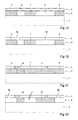
- FIGS. 1A to 1D The general aspects of the process of this The invention is described in relation to FIGS. 1A to 1D. of the examples of implementation of the process are described next for the realization of a transistor type SON and for the realization of a network of interconnections to connect the components of a circuit to each other.
- a substrate 1 forms on a substrate 1 a stack of a photosensitive layer 2 and a thin layer 3 of a given material.
- the substrate 1 can be any structure obtained after a step a standard method of forming integrated circuits. Stacking of the photosensitive layer 2 and the thin layer 3 can be obtained by various methods as will appear in the examples of implementation of the method of the present invention described below.
- the thin layer 3 can be composed of a dielectric, semiconductor or conductive material.
- sunstroke is carried out one or more portions of the photosensitive layer 2 with an electron beam passing through the thin layer 3.
- the penetration depth of the electron beam at through the thin layer 3, the photosensitive layer 2 and possibly the substrate 1 depends on the energy of acceleration of electrons, the respective thickness of the layers and their natures.
- Those skilled in the art will be able to define the thicknesses of layers 2 and 3 as well as the beam acceleration energy of electrons for insolating the photosensitive layer 2 all ensuring that the electron beam remains coherent in crossing the thin layer 3 in order to have a good definition insolated portions.
- the insolated portions of the photosensitive layer can be defined with an accuracy of less than 10 nm.
- FIG. 1A shows five portions 5, 6, 7, 8 and 9 from left to right. In the case where the photosensitive layer is positive, we insole the portions 6 and 8. In the case where the photosensitive layer is negative, the portions 5, 7 are and 9.
- portions 6 and 8 can be removed by an "evaporation" process.
- This method consists in placing the structure in a plasma which has the effect of modifying the structure of portions 6 and 8 without modifying that of portions 5, 7 and 9.
- the plasma used may be an oxygen (O 2 ) hydrogen (H 2 ) or nitrogen (N 2 ).
- O 2 oxygen
- H 2 hydrogen
- N 2 nitrogen
- FIG. 1B Another method of removing portions of the photosensitive layer 6 and 8 is illustrated in FIG. 1B.
- the opening 01 is formed above from the left side of portion 6 and extends above of the right-hand portion of portion 5.
- the O2 opening is formed above the middle portion of Portion 8.
- FIG. 1B openings of the thin layer 3 have been made above each of the portions of the photosensitive layer 2 that we want to eliminate.
- FIGS. 3F it is possible that the portions of the photosensitive layer that one wishes to delete are accessible "from side". In this case it is not essential to form openings prior to the elimination of certain portions of the layer photosensitive.
- an additional step, illustrated in FIG. 1D, of eliminating the remaining portions may be provided. of the photosensitive layer 6, 7 and 9.
- openings in this example O3 and O4, in the thin layer 3 above the portions to be eliminated, the portions 5 and 9 in this example.
- the type of photosensitive layer chosen allows it to be possible also to place the structure in a plasma (O 2 , H 2 , N 2 ) capable of modifying the structure of the portions 5, 7 and 9 of the photosensitive layer. so that the photosensitive layer is removed by passing through the thin layer 3.
- the portion 7 is removed through the thin layer 3.
- openings 03 and 04 there may be an additional step of filling the space previously occupied by the portions 5, 7 and 9 of a third material different from the second material.
- An advantage of the process of the present invention is it allows to form under a layer of a given material areas of emptiness and / or portions of another material of all the desired shapes.
- the insolation by a beam electrons being a very precise technique, the forms of Portions can be defined with great precision.
- Another advantage of the process of the present invention is that it does not damage the final portions or layers realized structures.
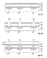
- FIG. 2 is a perspective view of a structure intermediate obtained after a step of a conventional method of forming transistors with surrounding grids.
- An active zone 100 of a semiconductor substrate 101 is delimited by a isolation region 102 formed on the surface of the substrate 101.
- active area 100 has in this example a substantially rectangular view from above.
- a layer of silicon forms a bridge 103 passing over the active zone 100 and relying on the isolation region 102 on both sides of the active zone 100.
- the portion of bridge 103 above the active zone 100 is monocrystalline, the portion located above the isolation region 102 is polycrystalline.
- Active area 100 and the bridge 103 are separated by a vacuum zone. Active area 100 is visible in plan view from each side of the deck 103.
- the structure represented in FIG. 2 is conventionally obtained by epitaxial growth of a silicon / germanium layer above the active zone 100 and epitaxial growth of a monocrystalline silicon layer above the layer of silicon germanium.
- the bilayer is then etched to forming a transverse band to the active zone 100.
- the portion remaining silicon germanium layer is removed by etching and thus the silicon bridge 103 is obtained.
- Figures 3A to 3F are sectional views of structures obtained after successive steps of an example of implementation of the method of the present invention carried out from the structure shown in Figure 2.
- the views in cut are made according to a plane cutting the bridge 103 longitudinally.
- a thin layer of silicon oxide SiO 2 is grown by thermal oxidation all around the silicon bridge 103 and on the active zone 100.
- a photosensitive layer 111 is then deposited above the structure and in the empty space between the bridge 103 and the active zone 100.
- the photosensitive layer 111 using an electron beam able to cross the photosensitive layer above the bridge 103, the bridge 103 covered with a thin layer of oxide of silicon and the photosensitive layer placed under the bridge 103.
- the photosensitive layer is positive, one insole a portion 120 of the photosensitive layer 111 located above of the central part of the bridge 103 and a portion 121 of the photosensitive layer 111 located directly above the portion 120 under deck 103. Portions, not shown, are also insulated. the photosensitive layer located in the extension portions 120 and 121 on each side of the bridge 103.
- insole portions 122 and 123 of the photosensitive layer located respectively above left and right parts of bridge 103 as well as portions 124 and 125 respectively below the parts of left and right of the bridge 103.
- insole portions of the photosensitive layer located in the extension of the portions 122 to 125 on each side of the bridge 123.
- a conductive material for example polycrystalline silicon, in the space previously occupied by portions 120 and 121 and the portions placed in the extension of the portions 120 and 121 on each side of the bridge 103.
- a conductive material for example polycrystalline silicon
- Portions of grid 130 and 131 respectively above and below the bridge 103 and grid portions, not shown, of each side of the bridge 103 in the extension of the portions 130 and 131. All of these portions constitute one and the same grid surrounding the bridge 103.
- next step illustrated in FIG. 3F, performs a nitride deposit so as to completely cover the previously obtained structure and to fill in the empty spaces situated under bridge 103 on both sides of section 131.
- On then performs anisotropic etching of the nitride up to discover the upper surface of grid portion 130, the thin oxide layer 110 placed on the deck 103 and the zone active 100 on both sides of the bridge 103.
- spacers 140 and 141 were formed on the flanks of portion 130 and portions 142 and 143 of nitride under the bridge 103 on either side of the grid portion 131.
- the portion of the bridge 103 between the silicon portions polycrystalline 130 and 131 is the channel of the transistor.
- the portions of bridge 103 located on both sides of canal 144 constitute source / drain zones 145 and 146.
- An advantage of the previously described method is that it allows for a surrounding gate transistor such as grid portions placed above and below the bridge of silicon are aligned.
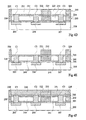
- a substrate 200 In an initial step, illustrated in FIG. 4A, form on a substrate 200 a stack of an insulating layer 201, a photosensitive layer 202 and an insulating layer 203.
- the substrate 200 can be any structure obtained after a step of a standard method of forming a integrated circuit.
- three conductive zones 205, 206 and 207 are shown at the surface of the substrate 200.
- the conductive zones 205, 206 and 207 are, for example, access terminals to integrated circuit components formed in the substrate 200.
- the insulating layers 201 and 203 may be thin layers of silicon oxide or layers of an insulator preferably having a low dielectric constant.
- openings O10, O11 and O12 in the stack of layers 201 203 above the conductive areas 205, 206 and 207.
- the openings O10, O11 and O12 may be formed according to a method comprising the following steps. Deposit a layer of nitride then a photosensitive layer on the insulating layer 203. On insole and removes portions of the photosensitive layer above conductive zones 205, 206 and 207. The unprotected portions of the nitride layer. We are serious successively the insulating layer 203, the photosensitive layer 202 and the insulating layer 201 according to an etching process anisotropic to form openings with walls substantially vertical. We finally eliminate the remaining portions the nitride layer.
- the filling of O10, O11 and O12 openings may consist of making a deposit of copper over the entire structure and then to perform a chemical mechanical polishing until discovering the insulating layer 203.
- the insulating layer 203 is then covered and the contacts C1, C2 and C3 of a photosensitive layer 210.
- the two layers of the photosensitive layer 202 and 210 with a electron beam passing through the photosensitive layer 210, the insulating layer 203 and the photosensitive layer 202.
- the photosensitive layer 210 we define in the photosensitive layer 210 five portions 220, 221, 222, 223 and 224 left to right and we define in the photosensitive layer 202 also five portions 230, 231, 232, 233 and 234 plumbed respectively portions 220 to 224.
- the portion 221 extends above contacts C1 and C2, the portion 223 is placed above contact C3.
- the photosensitive layer is positive, we insole the portions 221, 223, 231 and 233.
- the portions removed from the photosensitive layer are then replaced by vacuum zones 240 and 241.
- Another way to eliminate portions 231 and 233 is to form small openings in the insulating layer 203 above these portions, then remove them by wet etching.
- Training conductive lines can be carried out by depositing copper over the entire structure and polishing chemical mechanics until discovering the upper surface of portions 220, 222 and 224 of the photosensitive layer.
- the areas conductors 205 and 206 are then connected via contacts C1 and C2 and the conductive line 250.
- conductive lines can be repeated several times to form several levels of conductive lines.
- An advantage of the particular mode of implementation of the present invention is that it makes it possible to form a network of interconnections such that each conductive line is isolated other conductive lines by two very thin portions an insulating layer and a vacuum zone constituting the best insulation possible.
- the present invention is capable of various variations and modifications that will appear to man art.
- various methods can be implemented to form a stack of photosensitive layers and layers of one or more materials.
Landscapes
- Engineering & Computer Science (AREA)
- Microelectronics & Electronic Packaging (AREA)
- Power Engineering (AREA)
- Computer Hardware Design (AREA)
- Condensed Matter Physics & Semiconductors (AREA)
- General Physics & Mathematics (AREA)
- Physics & Mathematics (AREA)
- Ceramic Engineering (AREA)
- Manufacturing & Machinery (AREA)
- Crystallography & Structural Chemistry (AREA)
- Chemical & Material Sciences (AREA)
- Internal Circuitry In Semiconductor Integrated Circuit Devices (AREA)
- Exposure And Positioning Against Photoresist Photosensitive Materials (AREA)
- Photosensitive Polymer And Photoresist Processing (AREA)
- Exposure Of Semiconductors, Excluding Electron Or Ion Beam Exposure (AREA)
- Electron Beam Exposure (AREA)
- Thin Film Transistor (AREA)
- Materials For Photolithography (AREA)
Applications Claiming Priority (2)
| Application Number | Priority Date | Filing Date | Title |
|---|---|---|---|
| FR0350425A FR2858876B1 (fr) | 2003-08-12 | 2003-08-12 | Procede de formation sous une couche mince d'un premier materiau de portions d'un autre materiau et/ou de zones de vide |
| FR0350425 | 2003-08-12 |
Publications (3)
| Publication Number | Publication Date |
|---|---|
| EP1507286A2 true EP1507286A2 (de) | 2005-02-16 |
| EP1507286A3 EP1507286A3 (de) | 2007-07-11 |
| EP1507286B1 EP1507286B1 (de) | 2015-12-09 |
Family
ID=33561203
Family Applications (1)
| Application Number | Title | Priority Date | Filing Date |
|---|---|---|---|
| EP04103813.4A Not-in-force EP1507286B1 (de) | 2003-08-12 | 2004-08-06 | Herstellungsverfahren einer Netzwerkverbindung einer integrierten Schaltung und Herstellungsverfahren eines Transistors mit umschliessendem Gate |
Country Status (4)
| Country | Link |
|---|---|
| US (2) | US7202153B2 (de) |
| EP (1) | EP1507286B1 (de) |
| JP (1) | JP4572620B2 (de) |
| FR (1) | FR2858876B1 (de) |
Cited By (1)
| Publication number | Priority date | Publication date | Assignee | Title |
|---|---|---|---|---|
| FR2901058A1 (fr) * | 2006-08-29 | 2007-11-16 | St Microelectronics Crolles 2 | Dispositif a fonction dissymetrique et procede de realisation correspondant. |
Families Citing this family (10)
| Publication number | Priority date | Publication date | Assignee | Title |
|---|---|---|---|---|
| US7029964B2 (en) * | 2003-11-13 | 2006-04-18 | International Business Machines Corporation | Method of manufacturing a strained silicon on a SiGe on SOI substrate |
| EP1911098A1 (de) | 2005-06-30 | 2008-04-16 | Freescale Semiconductor, Inc. | Verfahren zur bildung einer halbleiterstruktur |
| KR100630764B1 (ko) * | 2005-08-30 | 2006-10-04 | 삼성전자주식회사 | 게이트 올어라운드 반도체소자 및 그 제조방법 |
| FR2900765B1 (fr) * | 2006-05-04 | 2008-10-10 | Commissariat Energie Atomique | Procede de realisation d'une grille de transistor comprenant une decomposition d'un materiau precurseur en au moins un materiau metallique, a l'aide d'au moins un faisceau d'electrons |
| US7871922B2 (en) * | 2007-04-10 | 2011-01-18 | Taiwan Semiconductor Manufacturing Co., Ltd. | Methods for forming interconnect structures that include forming air gaps between conductive structures |
| FR2921751B1 (fr) | 2007-10-02 | 2009-12-18 | St Microelectronics Crolles 2 | Procede de realisation de dispositif semi-conducteur a architecture asymetrique |
| FR2937463B1 (fr) | 2008-10-17 | 2010-12-24 | Commissariat Energie Atomique | Procede de fabrication de composants empiles et auto-alignes sur un substrat |
| FR2953991B1 (fr) * | 2009-12-10 | 2012-01-06 | Commissariat Energie Atomique | Procede de realisation d'un revetement de surface controle tridimensionnellement dans une cavite |
| FR3059148B1 (fr) | 2016-11-23 | 2019-09-06 | Commissariat A L'energie Atomique Et Aux Energies Alternatives | Realisation d'elements d'interconnexions auto-alignes pour circuit integre 3d |
| US11502106B2 (en) * | 2020-02-11 | 2022-11-15 | Globalfoundries U.S. Inc. | Multi-layered substrates of semiconductor devices |
Citations (5)
| Publication number | Priority date | Publication date | Assignee | Title |
|---|---|---|---|---|
| US4557995A (en) * | 1981-10-16 | 1985-12-10 | International Business Machines Corporation | Method of making submicron circuit structures |
| US4595649A (en) * | 1985-02-19 | 1986-06-17 | Allied Corporation | Glassy TiO2 polymer films as electron beam charge dissipation layers |
| FR2693030A1 (fr) * | 1992-06-26 | 1993-12-31 | Thomson Csf | Procédé de réalisation d'un transistor à effet de champ. |
| EP1091417A1 (de) * | 1999-10-05 | 2001-04-11 | STMicroelectronics S.A. | Herstellungsverfahren für Halbleiterbauelement mit Rundherum-Gate und dadurch hergestelltes Bauelement |
| US20030064577A1 (en) * | 2001-09-28 | 2003-04-03 | Hsu Sheng Teng | Method of making air gaps copper interconnect |
Family Cites Families (23)
| Publication number | Priority date | Publication date | Assignee | Title |
|---|---|---|---|---|
| US4092442A (en) * | 1976-12-30 | 1978-05-30 | International Business Machines Corporation | Method of depositing thin films utilizing a polyimide mask |
| JPS6378523A (ja) * | 1986-09-22 | 1988-04-08 | Hitachi Ltd | パタ−ン形成方法 |
| JP3460863B2 (ja) * | 1993-09-17 | 2003-10-27 | 三菱電機株式会社 | 半導体装置の製造方法 |
| ATE255769T1 (de) * | 1997-01-21 | 2003-12-15 | Georgia Tech Res Inst | Verfahren zur herstellung einer halbleitervorrichtung mit luftspalten für verbindungen mit ultraniedriger kapazität |
| US5851890A (en) * | 1997-08-28 | 1998-12-22 | Lsi Logic Corporation | Process for forming integrated circuit structure with metal silicide contacts using notched sidewall spacer on gate electrode |
| EP1074071A1 (de) * | 1998-04-20 | 2001-02-07 | Pulse Engineering, Inc. | Modularer mikroelektronischer stecker und methode |
| JP2000199968A (ja) * | 1999-01-06 | 2000-07-18 | Sony Corp | 多層レジスト構造およびこれを用いた3次元微細構造の作製方法 |
| US6071805A (en) * | 1999-01-25 | 2000-06-06 | Chartered Semiconductor Manufacturing, Ltd. | Air gap formation for high speed IC processing |
| US6207555B1 (en) * | 1999-03-17 | 2001-03-27 | Electron Vision Corporation | Electron beam process during dual damascene processing |
| JP3974319B2 (ja) * | 2000-03-30 | 2007-09-12 | 株式会社東芝 | エッチング方法 |
| US6287979B1 (en) * | 2000-04-17 | 2001-09-11 | Chartered Semiconductor Manufacturing Ltd. | Method for forming an air gap as low dielectric constant material using buckminsterfullerene as a porogen in an air bridge or a sacrificial layer |
| US6413852B1 (en) * | 2000-08-31 | 2002-07-02 | International Business Machines Corporation | Method of forming multilevel interconnect structure containing air gaps including utilizing both sacrificial and placeholder material |
| US20020187627A1 (en) * | 2001-06-06 | 2002-12-12 | Yu-Shen Yuang | Method of fabricating a dual damascene structure |
| US6919266B2 (en) * | 2001-07-24 | 2005-07-19 | Micron Technology, Inc. | Copper technology for ULSI metallization |
| DE10142223C2 (de) * | 2001-08-29 | 2003-10-16 | Infineon Technologies Ag | Verfahren zum Erzeugen von Hohlräumen mit Submikrometer-Abmessungen in einer Halbleitereinrichtung mittels Polymerisation |
| JP3504250B2 (ja) * | 2002-03-07 | 2004-03-08 | 沖電気工業株式会社 | 半導体素子の製造方法 |
| US6716741B2 (en) * | 2002-04-09 | 2004-04-06 | United Microelectronics Corp. | Method of patterning dielectric layer with low dielectric constant |
| US6734094B2 (en) * | 2002-04-29 | 2004-05-11 | Intel Corporation | Method of forming an air gap within a structure by exposing an ultraviolet sensitive material to ultraviolet radiation |
| US6867125B2 (en) * | 2002-09-26 | 2005-03-15 | Intel Corporation | Creating air gap in multi-level metal interconnects using electron beam to remove sacrificial material |
| US7294934B2 (en) * | 2002-11-21 | 2007-11-13 | Intel Corporation | Low-K dielectric structure and method |
| US6861332B2 (en) * | 2002-11-21 | 2005-03-01 | Intel Corporation | Air gap interconnect method |
| US6790788B2 (en) * | 2003-01-13 | 2004-09-14 | Applied Materials Inc. | Method of improving stability in low k barrier layers |
| US7456476B2 (en) * | 2003-06-27 | 2008-11-25 | Intel Corporation | Nonplanar semiconductor device with partially or fully wrapped around gate electrode and methods of fabrication |
-
2003
- 2003-08-12 FR FR0350425A patent/FR2858876B1/fr not_active Expired - Fee Related
-
2004
- 2004-08-06 EP EP04103813.4A patent/EP1507286B1/de not_active Not-in-force
- 2004-08-09 US US10/914,578 patent/US7202153B2/en active Active
- 2004-08-12 JP JP2004235362A patent/JP4572620B2/ja not_active Expired - Fee Related
-
2007
- 2007-02-28 US US11/712,353 patent/US8252638B2/en active Active
Patent Citations (5)
| Publication number | Priority date | Publication date | Assignee | Title |
|---|---|---|---|---|
| US4557995A (en) * | 1981-10-16 | 1985-12-10 | International Business Machines Corporation | Method of making submicron circuit structures |
| US4595649A (en) * | 1985-02-19 | 1986-06-17 | Allied Corporation | Glassy TiO2 polymer films as electron beam charge dissipation layers |
| FR2693030A1 (fr) * | 1992-06-26 | 1993-12-31 | Thomson Csf | Procédé de réalisation d'un transistor à effet de champ. |
| EP1091417A1 (de) * | 1999-10-05 | 2001-04-11 | STMicroelectronics S.A. | Herstellungsverfahren für Halbleiterbauelement mit Rundherum-Gate und dadurch hergestelltes Bauelement |
| US20030064577A1 (en) * | 2001-09-28 | 2003-04-03 | Hsu Sheng Teng | Method of making air gaps copper interconnect |
Non-Patent Citations (2)
| Title |
|---|
| CHIU G T ET AL: "ELECTRON DISCHARGING FOR ELECTRONBEAM EXPOSURE" IBM TECHNICAL DISCLOSURE BULLETIN, IBM CORP. NEW YORK, US, vol. 27, no. 8, janvier 1985 (1985-01), page 5014, XP000807789 ISSN: 0018-8689 * |
| PERSSON M, PETTERSSON J: "Submicron air-bridge interconnection process for complex gate geometries" J. VAC. SCI. TECHNOL. B, MICROELECTRON. NANOMETER STRUCT., vol. 15, no. 5, septembre 1997 (1997-09), pages 1724-1727, XP002283979 * |
Cited By (1)
| Publication number | Priority date | Publication date | Assignee | Title |
|---|---|---|---|---|
| FR2901058A1 (fr) * | 2006-08-29 | 2007-11-16 | St Microelectronics Crolles 2 | Dispositif a fonction dissymetrique et procede de realisation correspondant. |
Also Published As
| Publication number | Publication date |
|---|---|
| US20050037603A1 (en) | 2005-02-17 |
| US8252638B2 (en) | 2012-08-28 |
| EP1507286B1 (de) | 2015-12-09 |
| JP2005064517A (ja) | 2005-03-10 |
| US20070155159A1 (en) | 2007-07-05 |
| FR2858876B1 (fr) | 2006-03-03 |
| US7202153B2 (en) | 2007-04-10 |
| EP1507286A3 (de) | 2007-07-11 |
| FR2858876A1 (fr) | 2005-02-18 |
| JP4572620B2 (ja) | 2010-11-04 |
Similar Documents
| Publication | Publication Date | Title |
|---|---|---|
| EP0223780B1 (de) | Verfahren zum herstellen von mos-transistoren mit metallsilicidelektroden | |
| EP2009682B1 (de) | Vom Substrat isolierter Finfet-Feldeffekttransistor | |
| FR2853454A1 (fr) | Transistor mos haute densite | |
| EP0057126B1 (de) | Verfahren zur Herstellung einer Transistorstruktur | |
| FR2845203A1 (fr) | Transistor a effet de champ ayant de multiples canaux empiles et procede de fabrication | |
| FR2795555A1 (fr) | Procede de fabrication d'un dispositif semi-conducteur comprenant un empilement forme alternativement de couches de silicium et de couches de materiau dielectrique | |
| FR2661555A1 (fr) | Procede pour fabriquer un reseau-memoire a semi-conducteurs avec des cellules du type a grille flottante et sans contact. | |
| FR2618011A1 (fr) | Procede de fabrication d'une cellule de memoire | |
| FR2884052A1 (fr) | Transistor imos | |
| EP0351316B1 (de) | Verfahren zur Herstellung einer integrierten Speicher-Zelle | |
| WO2001001477A1 (fr) | Procede de gravure laterale par trous pour fabriquer des dispositifs semi-conducteurs | |
| EP1507286B1 (de) | Herstellungsverfahren einer Netzwerkverbindung einer integrierten Schaltung und Herstellungsverfahren eines Transistors mit umschliessendem Gate | |
| EP0461967A2 (de) | Halbleiteranordnung mit Schottky-Übergang für Mikrowellenverstärkung und schnelle logische Schaltungen und Verfahren zu deren Herstellung | |
| EP3550622B1 (de) | Integrierter schaltkreis mit bipolaren transistoren | |
| FR2894069A1 (fr) | Fabrication de transistors mos | |
| EP0414618B1 (de) | Dünnfilm-MOS-Transistor, bei dem die Kanalzone mit der Source verbunden ist, und Verfahren zur Herstellung | |
| WO2001026160A1 (fr) | Dispositif semi-conducteur combinant les avantages des architectures massives et soi, et procede de fabrication | |
| EP0190243B1 (de) | Verfahren zur herstellung einer integrierten schaltung vom mis-typ | |
| EP0949667A1 (de) | Elektrisch programmierbare Speicherzelle | |
| FR2885733A1 (fr) | Structure de transistor a trois grilles | |
| FR2718287A1 (fr) | Procédé de fabrication d'un transistor à effet de champ à grille isolée, en particulier de longueur de canal réduite, et transistor correspondant. | |
| EP3701567B1 (de) | Verfahren zur herstellung eines elektronischen bauteils mit doppelquantenpunkten | |
| FR2889622A1 (fr) | Procede de fabrication d'un transistor a nanodoigts semiconducteurs paralleles | |
| FR3055469A1 (fr) | Transistor a effet de champ a grille entourante | |
| FR3097076A1 (fr) | Prises de contact pour composant électronique |
Legal Events
| Date | Code | Title | Description |
|---|---|---|---|
| PUAI | Public reference made under article 153(3) epc to a published international application that has entered the european phase |
Free format text: ORIGINAL CODE: 0009012 |
|
| AK | Designated contracting states |
Kind code of ref document: A2 Designated state(s): AT BE BG CH CY CZ DE DK EE ES FI FR GB GR HU IE IT LI LU MC NL PL PT RO SE SI SK TR |
|
| AX | Request for extension of the european patent |
Extension state: AL HR LT LV MK |
|
| PUAL | Search report despatched |
Free format text: ORIGINAL CODE: 0009013 |
|
| AK | Designated contracting states |
Kind code of ref document: A3 Designated state(s): AT BE BG CH CY CZ DE DK EE ES FI FR GB GR HU IE IT LI LU MC NL PL PT RO SE SI SK TR |
|
| AX | Request for extension of the european patent |
Extension state: AL HR LT LV MK |
|
| 17P | Request for examination filed |
Effective date: 20080111 |
|
| AKX | Designation fees paid |
Designated state(s): AT BE BG CH CY CZ DE DK EE ES FI FR GB GR HU IE IT LI LU MC NL PL PT RO SE SI SK TR |
|
| 17Q | First examination report despatched |
Effective date: 20080616 |
|
| RAP1 | Party data changed (applicant data changed or rights of an application transferred) |
Owner name: COMMISSARIAT A L'ENERGIE ATOMIQUE |
|
| RAP1 | Party data changed (applicant data changed or rights of an application transferred) |
Owner name: COMMISSARIAT A L'ENERGIE ATOMIQUE ET AUX ENERGIES |
|
| GRAP | Despatch of communication of intention to grant a patent |
Free format text: ORIGINAL CODE: EPIDOSNIGR1 |
|
| RIC1 | Information provided on ipc code assigned before grant |
Ipc: H01L 29/66 20060101ALI20150611BHEP Ipc: H01L 21/027 20060101AFI20150611BHEP Ipc: H01L 29/786 20060101ALI20150611BHEP Ipc: H01L 21/768 20060101ALI20150611BHEP Ipc: H01L 29/423 20060101ALI20150611BHEP |
|
| INTG | Intention to grant announced |
Effective date: 20150713 |
|
| GRAS | Grant fee paid |
Free format text: ORIGINAL CODE: EPIDOSNIGR3 |
|
| GRAA | (expected) grant |
Free format text: ORIGINAL CODE: 0009210 |
|
| AK | Designated contracting states |
Kind code of ref document: B1 Designated state(s): AT BE BG CH CY CZ DE DK EE ES FI FR GB GR HU IE IT LI LU MC NL PL PT RO SE SI SK TR |
|
| REG | Reference to a national code |
Ref country code: GB Ref legal event code: FG4D Free format text: NOT ENGLISH |
|
| REG | Reference to a national code |
Ref country code: AT Ref legal event code: REF Ref document number: 764897 Country of ref document: AT Kind code of ref document: T Effective date: 20151215 Ref country code: CH Ref legal event code: EP |
|
| REG | Reference to a national code |
Ref country code: IE Ref legal event code: FG4D Free format text: LANGUAGE OF EP DOCUMENT: FRENCH |
|
| REG | Reference to a national code |
Ref country code: DE Ref legal event code: R096 Ref document number: 602004048334 Country of ref document: DE |
|
| REG | Reference to a national code |
Ref country code: NL Ref legal event code: MP Effective date: 20151209 |
|
| PG25 | Lapsed in a contracting state [announced via postgrant information from national office to epo] |
Ref country code: ES Free format text: LAPSE BECAUSE OF FAILURE TO SUBMIT A TRANSLATION OF THE DESCRIPTION OR TO PAY THE FEE WITHIN THE PRESCRIBED TIME-LIMIT Effective date: 20151209 |
|
| REG | Reference to a national code |
Ref country code: AT Ref legal event code: MK05 Ref document number: 764897 Country of ref document: AT Kind code of ref document: T Effective date: 20151209 |
|
| PG25 | Lapsed in a contracting state [announced via postgrant information from national office to epo] |
Ref country code: SE Free format text: LAPSE BECAUSE OF FAILURE TO SUBMIT A TRANSLATION OF THE DESCRIPTION OR TO PAY THE FEE WITHIN THE PRESCRIBED TIME-LIMIT Effective date: 20151209 Ref country code: NL Free format text: LAPSE BECAUSE OF FAILURE TO SUBMIT A TRANSLATION OF THE DESCRIPTION OR TO PAY THE FEE WITHIN THE PRESCRIBED TIME-LIMIT Effective date: 20151209 Ref country code: FI Free format text: LAPSE BECAUSE OF FAILURE TO SUBMIT A TRANSLATION OF THE DESCRIPTION OR TO PAY THE FEE WITHIN THE PRESCRIBED TIME-LIMIT Effective date: 20151209 Ref country code: GR Free format text: LAPSE BECAUSE OF FAILURE TO SUBMIT A TRANSLATION OF THE DESCRIPTION OR TO PAY THE FEE WITHIN THE PRESCRIBED TIME-LIMIT Effective date: 20160310 |
|
| PG25 | Lapsed in a contracting state [announced via postgrant information from national office to epo] |
Ref country code: IT Free format text: LAPSE BECAUSE OF FAILURE TO SUBMIT A TRANSLATION OF THE DESCRIPTION OR TO PAY THE FEE WITHIN THE PRESCRIBED TIME-LIMIT Effective date: 20151209 Ref country code: CZ Free format text: LAPSE BECAUSE OF FAILURE TO SUBMIT A TRANSLATION OF THE DESCRIPTION OR TO PAY THE FEE WITHIN THE PRESCRIBED TIME-LIMIT Effective date: 20151209 |
|
| PG25 | Lapsed in a contracting state [announced via postgrant information from national office to epo] |
Ref country code: PT Free format text: LAPSE BECAUSE OF FAILURE TO SUBMIT A TRANSLATION OF THE DESCRIPTION OR TO PAY THE FEE WITHIN THE PRESCRIBED TIME-LIMIT Effective date: 20160411 Ref country code: SK Free format text: LAPSE BECAUSE OF FAILURE TO SUBMIT A TRANSLATION OF THE DESCRIPTION OR TO PAY THE FEE WITHIN THE PRESCRIBED TIME-LIMIT Effective date: 20151209 Ref country code: RO Free format text: LAPSE BECAUSE OF FAILURE TO SUBMIT A TRANSLATION OF THE DESCRIPTION OR TO PAY THE FEE WITHIN THE PRESCRIBED TIME-LIMIT Effective date: 20151209 Ref country code: EE Free format text: LAPSE BECAUSE OF FAILURE TO SUBMIT A TRANSLATION OF THE DESCRIPTION OR TO PAY THE FEE WITHIN THE PRESCRIBED TIME-LIMIT Effective date: 20151209 Ref country code: AT Free format text: LAPSE BECAUSE OF FAILURE TO SUBMIT A TRANSLATION OF THE DESCRIPTION OR TO PAY THE FEE WITHIN THE PRESCRIBED TIME-LIMIT Effective date: 20151209 |
|
| REG | Reference to a national code |
Ref country code: FR Ref legal event code: PLFP Year of fee payment: 13 |
|
| REG | Reference to a national code |
Ref country code: DE Ref legal event code: R097 Ref document number: 602004048334 Country of ref document: DE |
|
| PLBE | No opposition filed within time limit |
Free format text: ORIGINAL CODE: 0009261 |
|
| STAA | Information on the status of an ep patent application or granted ep patent |
Free format text: STATUS: NO OPPOSITION FILED WITHIN TIME LIMIT |
|
| PG25 | Lapsed in a contracting state [announced via postgrant information from national office to epo] |
Ref country code: PL Free format text: LAPSE BECAUSE OF FAILURE TO SUBMIT A TRANSLATION OF THE DESCRIPTION OR TO PAY THE FEE WITHIN THE PRESCRIBED TIME-LIMIT Effective date: 20151209 Ref country code: DK Free format text: LAPSE BECAUSE OF FAILURE TO SUBMIT A TRANSLATION OF THE DESCRIPTION OR TO PAY THE FEE WITHIN THE PRESCRIBED TIME-LIMIT Effective date: 20151209 |
|
| 26N | No opposition filed |
Effective date: 20160912 |
|
| PG25 | Lapsed in a contracting state [announced via postgrant information from national office to epo] |
Ref country code: SI Free format text: LAPSE BECAUSE OF FAILURE TO SUBMIT A TRANSLATION OF THE DESCRIPTION OR TO PAY THE FEE WITHIN THE PRESCRIBED TIME-LIMIT Effective date: 20151209 |
|
| PG25 | Lapsed in a contracting state [announced via postgrant information from national office to epo] |
Ref country code: BE Free format text: LAPSE BECAUSE OF NON-PAYMENT OF DUE FEES Effective date: 20160831 |
|
| PG25 | Lapsed in a contracting state [announced via postgrant information from national office to epo] |
Ref country code: MC Free format text: LAPSE BECAUSE OF FAILURE TO SUBMIT A TRANSLATION OF THE DESCRIPTION OR TO PAY THE FEE WITHIN THE PRESCRIBED TIME-LIMIT Effective date: 20151209 |
|
| REG | Reference to a national code |
Ref country code: CH Ref legal event code: PL |
|
| PG25 | Lapsed in a contracting state [announced via postgrant information from national office to epo] |
Ref country code: LI Free format text: LAPSE BECAUSE OF NON-PAYMENT OF DUE FEES Effective date: 20160831 Ref country code: CH Free format text: LAPSE BECAUSE OF NON-PAYMENT OF DUE FEES Effective date: 20160831 |
|
| REG | Reference to a national code |
Ref country code: IE Ref legal event code: MM4A |
|
| PG25 | Lapsed in a contracting state [announced via postgrant information from national office to epo] |
Ref country code: IE Free format text: LAPSE BECAUSE OF NON-PAYMENT OF DUE FEES Effective date: 20160806 |
|
| PG25 | Lapsed in a contracting state [announced via postgrant information from national office to epo] |
Ref country code: LU Free format text: LAPSE BECAUSE OF NON-PAYMENT OF DUE FEES Effective date: 20160806 |
|
| REG | Reference to a national code |
Ref country code: FR Ref legal event code: PLFP Year of fee payment: 14 |
|
| PG25 | Lapsed in a contracting state [announced via postgrant information from national office to epo] |
Ref country code: CY Free format text: LAPSE BECAUSE OF FAILURE TO SUBMIT A TRANSLATION OF THE DESCRIPTION OR TO PAY THE FEE WITHIN THE PRESCRIBED TIME-LIMIT Effective date: 20151209 Ref country code: HU Free format text: LAPSE BECAUSE OF FAILURE TO SUBMIT A TRANSLATION OF THE DESCRIPTION OR TO PAY THE FEE WITHIN THE PRESCRIBED TIME-LIMIT; INVALID AB INITIO Effective date: 20040806 |
|
| PG25 | Lapsed in a contracting state [announced via postgrant information from national office to epo] |
Ref country code: TR Free format text: LAPSE BECAUSE OF FAILURE TO SUBMIT A TRANSLATION OF THE DESCRIPTION OR TO PAY THE FEE WITHIN THE PRESCRIBED TIME-LIMIT Effective date: 20151209 |
|
| PG25 | Lapsed in a contracting state [announced via postgrant information from national office to epo] |
Ref country code: BG Free format text: LAPSE BECAUSE OF FAILURE TO SUBMIT A TRANSLATION OF THE DESCRIPTION OR TO PAY THE FEE WITHIN THE PRESCRIBED TIME-LIMIT Effective date: 20151209 |
|
| REG | Reference to a national code |
Ref country code: FR Ref legal event code: PLFP Year of fee payment: 15 |
|
| PGFP | Annual fee paid to national office [announced via postgrant information from national office to epo] |
Ref country code: DE Payment date: 20180813 Year of fee payment: 15 Ref country code: FR Payment date: 20180830 Year of fee payment: 15 |
|
| PGFP | Annual fee paid to national office [announced via postgrant information from national office to epo] |
Ref country code: GB Payment date: 20180821 Year of fee payment: 15 |
|
| REG | Reference to a national code |
Ref country code: DE Ref legal event code: R119 Ref document number: 602004048334 Country of ref document: DE |
|
| GBPC | Gb: european patent ceased through non-payment of renewal fee |
Effective date: 20190806 |
|
| PG25 | Lapsed in a contracting state [announced via postgrant information from national office to epo] |
Ref country code: DE Free format text: LAPSE BECAUSE OF NON-PAYMENT OF DUE FEES Effective date: 20200303 Ref country code: FR Free format text: LAPSE BECAUSE OF NON-PAYMENT OF DUE FEES Effective date: 20190831 |
|
| PG25 | Lapsed in a contracting state [announced via postgrant information from national office to epo] |
Ref country code: GB Free format text: LAPSE BECAUSE OF NON-PAYMENT OF DUE FEES Effective date: 20190806 |