EP1503404B1 - Präzise Strukturierung von Schichten mit hoher Dielektrizitätskonstante - Google Patents
Präzise Strukturierung von Schichten mit hoher Dielektrizitätskonstante Download PDFInfo
- Publication number
- EP1503404B1 EP1503404B1 EP04017471A EP04017471A EP1503404B1 EP 1503404 B1 EP1503404 B1 EP 1503404B1 EP 04017471 A EP04017471 A EP 04017471A EP 04017471 A EP04017471 A EP 04017471A EP 1503404 B1 EP1503404 B1 EP 1503404B1
- Authority
- EP
- European Patent Office
- Prior art keywords
- gate
- layer
- trench
- dielectric material
- dielectric layer
- Prior art date
- Legal status (The legal status is an assumption and is not a legal conclusion. Google has not performed a legal analysis and makes no representation as to the accuracy of the status listed.)
- Expired - Lifetime
Links
Images


Classifications
-
- H—ELECTRICITY
- H10—SEMICONDUCTOR DEVICES; ELECTRIC SOLID-STATE DEVICES NOT OTHERWISE PROVIDED FOR
- H10P—GENERIC PROCESSES OR APPARATUS FOR THE MANUFACTURE OR TREATMENT OF DEVICES COVERED BY CLASS H10
- H10P50/00—Etching of wafers, substrates or parts of devices
- H10P50/60—Wet etching
- H10P50/61—Electrolytic etching
- H10P50/613—Electrolytic etching of Group IV materials
-
- H—ELECTRICITY
- H10—SEMICONDUCTOR DEVICES; ELECTRIC SOLID-STATE DEVICES NOT OTHERWISE PROVIDED FOR
- H10D—INORGANIC ELECTRIC SEMICONDUCTOR DEVICES
- H10D64/00—Electrodes of devices having potential barriers
- H10D64/01—Manufacture or treatment
- H10D64/013—Manufacture or treatment of electrodes having a conductor capacitively coupled to a semiconductor by an insulator
- H10D64/01302—Manufacture or treatment of electrodes having a conductor capacitively coupled to a semiconductor by an insulator the insulator being formed after the semiconductor body, the semiconductor being silicon
- H10D64/01304—Manufacture or treatment of electrodes having a conductor capacitively coupled to a semiconductor by an insulator the insulator being formed after the semiconductor body, the semiconductor being silicon characterised by the conductor
- H10D64/01326—Aspects related to lithography, isolation or planarisation of the conductor
-
- H—ELECTRICITY
- H10—SEMICONDUCTOR DEVICES; ELECTRIC SOLID-STATE DEVICES NOT OTHERWISE PROVIDED FOR
- H10P—GENERIC PROCESSES OR APPARATUS FOR THE MANUFACTURE OR TREATMENT OF DEVICES COVERED BY CLASS H10
- H10P50/00—Etching of wafers, substrates or parts of devices
- H10P50/20—Dry etching; Plasma etching; Reactive-ion etching
- H10P50/28—Dry etching; Plasma etching; Reactive-ion etching of insulating materials
- H10P50/282—Dry etching; Plasma etching; Reactive-ion etching of insulating materials of inorganic materials
- H10P50/283—Dry etching; Plasma etching; Reactive-ion etching of insulating materials of inorganic materials by chemical means
Definitions
- This invention relates to fabricating microelectronic devices, and more particularly to precision formation of a trench in a dielectric layer.
- Microelectronic structures such as semiconductor structures, may be created by forming layers and trenches in various structural configurations from various materials.
- One of the challenges associated with conventional techniques utilized for patterning dielectric films, such as high dielectric constant, or "high-K", films is trenching with accuracy to avoid damage to the integrity of adjacent structures.
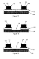
- FIG 1A a cross-sectional view of a typical gate structure is depicted wherein two gates (104, 106) with spacers (108, 110, 112, 114) are formed adjacent a high-K gate oxide layer (102), which is formed adjacent a substrate layer (100).
- Figure 1B depicts an undesirable patterning scenario wherein dry etching techniques have been utilized, resulting in a trench (116) that is overdeep.
- FIG. 1B depicts another undesirable patterning scenario wherein wet etching has been utilized, resulting in a trench (118) that undesirably undercuts neighboring structures such as gates (104, 106) and spacers (110, 112).
- Many wet etching treatments are associated with substantially isotropic etch rate characteristics, resulting in negative etch bias and undercutting, as depicted, for example, in Figure 1C .
- US Patent US 6,432,779 B1 discloses a method for forming a semiconductor device in which a metal oxide gate dielectric layer is formed over a substrate. A gate electrode is then formed over the metal oxide layer thereby exposing a portion of the metal oxide layer. The formation of the gate electrode further includes forming narrow spacer structures adjacent the sidewalls of the gate electrode. The exposed portion of the metal oxide gate dielectrode layer is then chemically reduced to metal or a metal hydride. The metal or metal hydride is then removed with a conventional wet etch or wet/dry etch combination.
- the invention is defined by a method according to claim 1.
- Figures 1A-1C are cross-sectional depictions of conventional substrate patterning treatment.
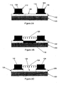
- Figures 2A-2C are cross sectional views of various aspects of a patterning treatment of an embodiment of the present invention.
- Figure 3 is a flowchart depicting various stages of a patterning treatment of an embodiment of the present invention.
- Figures 4A-4D are cross sectional views of various aspects of a patterning treatment of a second embodiment of the present invention.
- Figure 5 is a flowchart depicting various stages of a patterning treatment of the second embodiment of the present invention.
- Figures 2A-2C are cross sectional views of various aspects of a patterning treatment of one embodiment not being part of the present invention.
- a microelectronic structure similar to that depicted in Figure 1A is shown.
- Such a structure may be formed utilizing various techniques and materials.
- a high-K dielectric layer (102) may be formed upon a substrate layer (100) using techniques such as chemical or physical vapor deposition or other techniques.
- the high-K dielectric layer (102) may comprise a high-K material such as hafnium dioxide, zirconium dioxide, or silicate derivatives thereof
- the substrate layer (100) may comprise a semiconducting material such as silicon, or another material.
- gates (104, 106) may be formed between spacers (108, 110, 112, 114).
- the gates (104, 106) comprise a gate material such as polysilicon and the spacers (108, 110, 112, 114) comprise a spacer material such as silicon nitride, although other materials may be used in other embodiments.
- a portion (132) of the high-K dielectric layer (102) surface remains exposed.
- the exposed high-K dielectric layer surface (132) is exposed to hydrogen (120), resulting in a hydrogen reduction reaction.
- Reduction of d-block (between groups II and III on the Periodic Table) transition metal complexes/films with molecular hydrogen to the corresponding metallic species is a well-known phenomenon, described, for example, in publications such as " Chemistry of the Elements", 2nd Edition, by N. N. Greenwood and A. Earnshaw, 1997 .
- the exposed surface (132) is exposed to hydrogen (120) in a parallel plate plasma chamber, where a device wafer that includes the gates (104, 106), high-K dielectric layer (102), and substrate layer (100) acts as one plate, and is spaced in a range of about 5 mm to about 10 mm from a second plate.
- a radio frequency (“RF") power source with a power density in a range of about 2 W/cm 2 to about 4 W/cm 2 , and a frequency in a range of about 200 kHz to about 13.5 MHz.
- the temperature of the wafer is in a range from about 20° C to about 450° C.
- the chamber has a pressure in a range of about 1 Torr to about 2 Torr.
- Other embodiments may use different conditions to perform the hydrogen reduction reaction.
- the hydrogen reduction reaction may be notated as follows: HfO 2 + 2 ⁇ H 2 ⁇ Hf + 2 ⁇ H 2 ⁇ O
- the result of the reduction reaction is a reduced portion (122) of the high-K gate dielectric layer (102).
- the reduced, or "converted" portion (122), now a metallic substance may be selectively removed, as depicted in Figure 2C , via exposure to a wet etch chemistry (124) selective to the converted metallic, such as the sulfuric acid and hydrogen peroxide based etch chemistry known as a "piranha” etch chemistry, or a hydrochloric acid and hydrogen peroxide based wet etch chemistry known as an "SC2" or "RCA standard clean 2" wet etch chemistry, to leave behind a trench (126). Removal of the reduced portion (122) also results in remaining discrete portions (128, 130) of the high-K dielectric layer (102).
- the trench (126) is without substantial negative etch bias or damage to the underlying substrate layer (100) due to the relatively high selectivity of such wet etch chemistry (124) to metallics as opposed to other adjacent nonmetallic materials, including adjacent portions of the high-K gate dielectric (102) which have not been reduced or converted. Indeed, the trench (126) resulting from the removal of reduced material (122) is substantially straight with substantially parallel walls - also known in the art as a trench having substantially zero positive or negative "etch bias.”
- Wet etch chemistries (124) such as piranha and SC2 are well known in the art as systems for selectively removing organics and metallics to reach underlying metallic or substrate materials.
- a low pH system with an oxidant such as hydrochloric acid with peroxide as in the SC2 etch chemistry
- an oxidant such as hydrochloric acid with peroxide as in the SC2 etch chemistry
- other methods such as an aqueous solution of a common chelating agent, derivatives of phosphonates or ethylenediaminetetraacetic acid for example, may be used to selectively remove the reduced portion (122).
- the dielectric layer (102) is patterned with precision to avoid problems with eroding an underlying substrate layer (100) and undercutting adjacent structures, such as gates (104, 106) or spacers (108, 110, 112, 114).
- a flowchart summarizing a patterning treatment of one embodiment not being part of the present invention is depicted, wherein a high-K gate dielectric layer is formed (300) adjacent a substrate layer, subsequent to which gates and spacers are formed (302) adjacent the high-K gate dielectric layer, leaving an exposed surface of the high-K gate dielectric layer.
- the exposed high-K gate dielectric layer surface is exposed (304) to hydrogen gas, which leads to a reduction reaction.
- the reduced high-K gate dielectric material is etched (306) to form a trench by a wet etch chemistry that is selective to the reduced high-K gate dielectric material so that the reduced gate dielectric material is selectively removed without substantially undercutting adjacent gate structures or substantially eroding underlying substrate layer materials.
- Figures 4A-4D are cross sectional views of various aspects of a patterning treatment of a second embodiment of the present invention.
- a microelectronic structure similar to that depicted in Figure 2A is shown. However, the structure in Figure 4A does not include spacers (108, 110, 112, 114) adjacent the gates (104, 106).
- Such a structure may be formed utilizing various techniques and materials. For example, a high-K dielectric layer (102) may be formed upon a substrate layer (100) using techniques such as chemical or physical vapor deposition or other techniques.
- the high-K dielectric layer (102) may comprise a high-K material such as hafnium dioxide, zirconium dioxide, or silicate derivatives thereof, and the substrate layer (100) may comprise a semiconducting material such as silicon, or another material.
- gates (104, 106) may be formed on the high-K dielectric layer (102).
- the gates (104, 106) comprise a gate material such as polysilicon, although other materials may be used in other embodiments.
- a portion (132) of the high-K dielectric layer (102) between the gates (104, 106) remains exposed.
- the exposed high-K dielectric layer surface (132) is exposed to hydrogen (120), resulting in a hydrogen reduction reaction.
- this exposure is performed similarly to the exposure described above with respect to Figure 2B , with the same result of a reduced portion (122) of the high-K gate dielectric layer (102).
- the reduced, or "converted" portion (122), now a metallic substance may be selectively removed, as depicted in Figure 4C , via exposure to a wet etch chemistry (124) selective to the converted metallic to leave behind a trench (126).
- This wet etch chemistry (124) is typically performed in the same manner as described above with respect to Figure 2C .
- the trench (126) is without substantial negative etch bias or damage to the underlying substrate layer (100) due to the relatively high selectivity of such wet etch chemistry (124) to metallics as opposed to other adjacent nonmetallic materials, including adjacent portions of the high-K gate dielectric (102) which have not been reduced or converted.
- the trench (126) resulting from the removal of reduced material (122) is substantially straight with substantially parallel walls - also known in the art as a trench having substantially zero positive or negative "etch bias.”
- the dielectric layer (102) is patterned with precision to avoid problems with eroding an underlying substrate layer (100) and undercutting adjacent structures, such as gates (104, 106).
- spacers (108, 110, 112, 114) are then formed adjacent to the gates (104, 106) and the discrete portions (128, 130) of the high-K dielectric layer (102).
- spacers (110, 112) are formed adjacent to both gates (104, 106) and discrete portions (128, 130) of the high-K dielectric layer (102), and extend from substantially a top surface of the gates (104, 106) into the trench (126) and to a top surface of material exposed by removal of the reduced portion (122) of the high-K dielectric layer (102).
- the top surface of material exposed by removal of the reduced portion (122) of the high-K dielectric layer is the bottom surface of the trench, which is the top surface of the substrate layer (100) in the illustrated embodiment.
- a trench (126) is formed on one side of each of the gates (104, 106).
- the high-K dielectric layer (102) remains on a non-trench side of the gates (104, 106).
- spacers (108, 114) on the non-trench side of the gates (104, 106) are formed adjacent to the gates (104, 106) and extend from substantially the top surface of the gates (104, 106) to top surfaces of the discrete portions (128, 130) of the high-K dielectric layer (102).
- trenches (126) may be formed on both sides of one or both of the gates (104, 106).
- one or both of spacers (108, 114) on the non-trench side of the gates (104, 106) may also be formed adjacent to both gates (104, 106) and discrete portions (128, 130) of the high-K dielectric layer (102), and extend from substantially a top surface of the gates (104, 106) into the trench (126) and to a top surface of the substrate layer (100) exposed by removal of the reduced portion (122) of the high-K dielectric layer (102).
- the dielectric layer (102) is patterned with precision to avoid problems with eroding an underlying substrate layer (100) and undercutting adjacent structures, such as gates (104, 106) or spacers (108, 110, 112, 114).
- a flowchart summarizing a patterning treatment of one embodiment of the present invention is depicted, wherein a high-K gate dielectric layer is formed (500) adjacent a substrate layer, subsequent to which gates are formed (502) adjacent the high-K gate dielectric layer, leaving an exposed surface of the high-K gate dielectric layer.
- the exposed high-K gate dielectric layer surface is exposed (504) to hydrogen gas, which leads to a reduction reaction.
- the reduced high-K gate dielectric material is etched (506) to form a trench by a wet etch chemistry that is selective to the reduced high-K gate dielectric material so that the reduced gate dielectric material is selectively removed without substantially undercutting adjacent gate structures or substantially eroding underlying substrate layer materials.
- spacers are formed (508) adjacent the gates and a portion of the remaining high-K gate dielectric layer. On sides of the gates adjacent the trench, these spacers extend substantially from the top surface of the gates to the top surface of the substrate layer.
Landscapes
- Insulated Gate Type Field-Effect Transistor (AREA)
- Drying Of Semiconductors (AREA)
- Weting (AREA)
- Electrodes Of Semiconductors (AREA)
- Insulating Bodies (AREA)
- Laminated Bodies (AREA)
Claims (10)
- Verfahren, das folgende Schritte umfasst:Bilden einer Schicht aus dielektrischem Hoch-k-Material (102) auf einer Schicht eines Substratmaterials (100);Bilden mindestens eines ersten Gates (104) und eines zweiten Gates (106) auf der Schicht aus dem dielektrischen Hoch-k-Material (102), Übriglassen eines freiliegenden Teils (132) des Hoch-k-Materials (102) zwischen dem ersten und dem zweiten Gate;Aussetzen des freiliegenden Teils (132) der Schicht aus dem dielektrischen Hoch-k-Material (102) an Wasserstoff, um den freiliegenden Teil zu reduzieren, um einen metallischen Teil (122) aus dem freiliegenden Teil zu bilden;Entfernen des metallischen Teils (122) von der Schicht aus dem Hoch-k-Material durch Aussetzen des metallischen Teils an ein chemisches Nassätzmittel, das für den metallischen Teil selektiv ist, um einen Graben (126) zwischen dem ersten Gate und dem zweiten Gate zu bilden, während getrennte Teile (128, 130) des Hoch-k-Materials an Seiten des ersten und zweiten Gates gegenüberliegend dem Graben übriggelassen werden;Bilden von ersten Abstandshaltern (110, 112), einen (110) auf einer Seite des ersten Gates (104) benachbart zum Graben (126) und einen weiteren (112) auf einer Seite des zweiten Gates (106) benachbart zum Graben (126), wobei sich die ersten Abstandshalter von im Wesentlichen einer oberen Oberfläche des Gates zu einer unteren Oberfläche des Grabens erstrecken;Bilden von zweiten Abstandshaltern (108, 114), einen (108) auf einer Seite des ersten Gates (104) gegenüberliegend dem Graben (126) und einen weiteren (114) auf einer Seite des zweiten Gates (106) gegenüberliegend dem Graben (126), wobei sich die zweiten Abstandshalter von im Wesentlichen der oberen Oberfläche des Gates zu der oberen Oberfläche des getrennten Teils des Hoch-k-Materials erstrecken.
- Verfahren nach Anspruch 1, wobei das dielektrische Hoch-k-Material Hafnium-Dioxid und der metallische Teil Hafnium umfasst.
- Verfahren nach Anspruch 1, wobei das dielektrische Hoch-k-Material ZirkoniumDioxid und der metallische Teil Zirkonium umfasst.
- Verfahren nach Anspruch 1, wobei das Aussetzen des freiliegenden Teils der Schicht aus dem dielektrischen Hoch-k-Material an Wasserstoff ein Aussetzen des freiliegenden Teils der Schicht aus dem dielektrischen High-K-Material an Wasserstoff in einer Plasmakammer umfasst.
- Verfahren nach Anspruch 4, wobei die Schicht aus dem dielektrischen Hoch-k-Material in der Plasmakammer mit einem Abstand von einer Platte im Bereich von ungefähr 5mm bis ungefähr 10mm abgeschieden wird.
- Verfahren nach Anspruch 4, wobei das Aussetzen des freiliegenden Teils der Schicht aus dem dielektrischen Hoch-k-Material an Wasserstoff ein Aussetzen des freiliegenden Teils der Schicht aus dem dielektrischen Hoch-k-Material an Wasserstoff mit einer Flussrate im Bereich von ungefähr 1000 SCCM bis ungefähr 2000 SCCM umfasst.
- Verfahren nach Anspruch 1, wobei das chemische Nassätzmittel eine schwefelsäure- und wasserstoffperoxidbasierte Ätzchemie umfasst.
- Verfahren nach Anspruch 7, wobei die Ätzchemie eine Piranha-Ätzchemie ist.
- Verfahren nach Anspruch 1, wobei das chemische Nassätzmittel eine chlorwasserstoffsäure- und wasserstoffperoxidbasierte Ätzchemie umfasst.
- Verfahren nach Anspruch 9, wobei die Ätzchemie eine SC2-Ätzchemie ist.
Applications Claiming Priority (2)
| Application Number | Priority Date | Filing Date | Title |
|---|---|---|---|
| US10/632,470 US6855639B1 (en) | 2003-08-01 | 2003-08-01 | Precise patterning of high-K films |
| US632470 | 2003-08-01 |
Publications (3)
| Publication Number | Publication Date |
|---|---|
| EP1503404A2 EP1503404A2 (de) | 2005-02-02 |
| EP1503404A3 EP1503404A3 (de) | 2005-04-06 |
| EP1503404B1 true EP1503404B1 (de) | 2009-12-02 |
Family
ID=33541545
Family Applications (1)
| Application Number | Title | Priority Date | Filing Date |
|---|---|---|---|
| EP04017471A Expired - Lifetime EP1503404B1 (de) | 2003-08-01 | 2004-07-23 | Präzise Strukturierung von Schichten mit hoher Dielektrizitätskonstante |
Country Status (8)
| Country | Link |
|---|---|
| US (2) | US6855639B1 (de) |
| EP (1) | EP1503404B1 (de) |
| KR (1) | KR100592841B1 (de) |
| CN (1) | CN100336181C (de) |
| AT (1) | ATE450887T1 (de) |
| DE (1) | DE602004024355D1 (de) |
| TW (1) | TWI320204B (de) |
| WO (1) | WO2005013347A2 (de) |
Families Citing this family (15)
| Publication number | Priority date | Publication date | Assignee | Title |
|---|---|---|---|---|
| JP4040425B2 (ja) * | 2002-10-17 | 2008-01-30 | Necエレクトロニクス株式会社 | 半導体装置の製造方法 |
| US20050064716A1 (en) * | 2003-04-14 | 2005-03-24 | Hong Lin | Plasma removal of high k metal oxide |
| US7413996B2 (en) * | 2003-04-14 | 2008-08-19 | Lsi Corporation | High k gate insulator removal |
| US7037845B2 (en) * | 2003-08-28 | 2006-05-02 | Intel Corporation | Selective etch process for making a semiconductor device having a high-k gate dielectric |
| US7160779B2 (en) * | 2005-02-23 | 2007-01-09 | Intel Corporation | Method for making a semiconductor device having a high-k gate dielectric |
| US20060220090A1 (en) * | 2005-03-23 | 2006-10-05 | Intel Corporation | Semiconductor device with a high-k gate dielectric and a metal gate electrode |
| US7449756B2 (en) * | 2005-06-13 | 2008-11-11 | Intel Corporation | Semiconductor device with a high-k gate dielectric and a metal gate electrode |
| US7501336B2 (en) * | 2005-06-21 | 2009-03-10 | Intel Corporation | Metal gate device with reduced oxidation of a high-k gate dielectric |
| US7595248B2 (en) * | 2005-12-01 | 2009-09-29 | Intel Corporation | Angled implantation for removal of thin film layers |
| US7226831B1 (en) | 2005-12-27 | 2007-06-05 | Intel Corporation | Device with scavenging spacer layer |
| US7659178B2 (en) * | 2006-04-21 | 2010-02-09 | International Business Machines Corporation | Semiconductor device structures with reduced junction capacitance and drain induced barrier lowering and methods for fabricating such device structures and for fabricating a semiconductor-on-insulator substrate |
| US7984408B2 (en) * | 2006-04-21 | 2011-07-19 | International Business Machines Corporation | Structures incorporating semiconductor device structures with reduced junction capacitance and drain induced barrier lowering |
| US20070262399A1 (en) * | 2006-05-10 | 2007-11-15 | Gilbert Dewey | Sealing spacer to reduce or eliminate lateral oxidation of a high-k gate dielectric |
| KR100973828B1 (ko) * | 2008-05-09 | 2010-08-03 | 포항공과대학교 산학협력단 | 금속 박막의 증착을 이용한 유리 나노 가공 방법 |
| US8853076B2 (en) | 2012-09-10 | 2014-10-07 | International Business Machines Corporation | Self-aligned contacts |
Family Cites Families (12)
| Publication number | Priority date | Publication date | Assignee | Title |
|---|---|---|---|---|
| JPS5424236A (en) * | 1977-07-25 | 1979-02-23 | Sharp Corp | Etching solution and minute working process |
| US4980032A (en) * | 1988-08-12 | 1990-12-25 | Alameda Instruments, Inc. | Distillation method and apparatus for reprocessing sulfuric acid |
| USRE35827E (en) * | 1989-05-02 | 1998-06-23 | Sgs-Thomson Microelectronics S.R.L. | Surface field effect transistor with depressed source and/or drain areas for ULSI integrated devices |
| JP2961494B2 (ja) * | 1994-07-15 | 1999-10-12 | キヤノン株式会社 | 電子放出素子、電子源、及びそれを用いた画像形成装置の製造方法 |
| US6124620A (en) * | 1998-05-14 | 2000-09-26 | Advanced Micro Devices, Inc. | Incorporating barrier atoms into a gate dielectric using gas cluster ion beam implantation |
| US6017790A (en) * | 1998-07-06 | 2000-01-25 | United Microelectronics Corp. | Method of manufacturing embedded dynamic random access memory |
| JP2001213696A (ja) * | 1999-11-22 | 2001-08-07 | Shin Etsu Handotai Co Ltd | エピタキシャルウェーハの製造方法およびこれに用いる半導体製造装置 |
| US6432779B1 (en) * | 2000-05-18 | 2002-08-13 | Motorola, Inc. | Selective removal of a metal oxide dielectric |
| US6300202B1 (en) * | 2000-05-18 | 2001-10-09 | Motorola Inc. | Selective removal of a metal oxide dielectric |
| US6544906B2 (en) * | 2000-12-21 | 2003-04-08 | Texas Instruments Incorporated | Annealing of high-k dielectric materials |
| US7887711B2 (en) * | 2002-06-13 | 2011-02-15 | International Business Machines Corporation | Method for etching chemically inert metal oxides |
| US6794721B2 (en) * | 2002-12-23 | 2004-09-21 | International Business Machines Corporation | Integration system via metal oxide conversion |
-
2003
- 2003-08-01 US US10/632,470 patent/US6855639B1/en not_active Expired - Lifetime
-
2004
- 2004-07-20 CN CNB2004100708261A patent/CN100336181C/zh not_active Expired - Fee Related
- 2004-07-21 WO PCT/US2004/023568 patent/WO2005013347A2/en not_active Ceased
- 2004-07-22 TW TW093121973A patent/TWI320204B/zh not_active IP Right Cessation
- 2004-07-23 AT AT04017471T patent/ATE450887T1/de not_active IP Right Cessation
- 2004-07-23 DE DE602004024355T patent/DE602004024355D1/de not_active Expired - Lifetime
- 2004-07-23 EP EP04017471A patent/EP1503404B1/de not_active Expired - Lifetime
- 2004-07-30 KR KR1020040060505A patent/KR100592841B1/ko not_active Expired - Fee Related
- 2004-12-20 US US11/018,015 patent/US20050110072A1/en not_active Abandoned
Also Published As
| Publication number | Publication date |
|---|---|
| WO2005013347A2 (en) | 2005-02-10 |
| US20050026451A1 (en) | 2005-02-03 |
| EP1503404A2 (de) | 2005-02-02 |
| EP1503404A3 (de) | 2005-04-06 |
| CN1581446A (zh) | 2005-02-16 |
| US20050110072A1 (en) | 2005-05-26 |
| KR20050016077A (ko) | 2005-02-21 |
| ATE450887T1 (de) | 2009-12-15 |
| TW200518224A (en) | 2005-06-01 |
| CN100336181C (zh) | 2007-09-05 |
| US6855639B1 (en) | 2005-02-15 |
| DE602004024355D1 (de) | 2010-01-14 |
| WO2005013347A3 (en) | 2005-04-28 |
| TWI320204B (en) | 2010-02-01 |
| KR100592841B1 (ko) | 2006-06-26 |
Similar Documents
| Publication | Publication Date | Title |
|---|---|---|
| EP1503404B1 (de) | Präzise Strukturierung von Schichten mit hoher Dielektrizitätskonstante | |
| JP4554461B2 (ja) | 半導体装置の製造方法 | |
| CN1273866C (zh) | 镶嵌蚀刻方法中各向异性氮化物的蚀刻工艺 | |
| US5872063A (en) | Self-aligned contact structures using high selectivity etching | |
| KR100291154B1 (ko) | 폴리사이드막의드라이에칭방법 | |
| US9780000B2 (en) | Method for forming spacers for a transitor gate | |
| JP3248072B2 (ja) | 酸化膜エッチング方法 | |
| US6027959A (en) | Methods for in-situ removal of an anti-reflective coating during a nitride resistor protect etching process | |
| US6066567A (en) | Methods for in-situ removal of an anti-reflective coating during an oxide resistor protect etching process | |
| CN101459060B (zh) | 半导体装置的制造方法 | |
| KR20010075177A (ko) | 집적 회로 게이트 전도체 위에 형성된 스페이서를식각하기 위한 디바이스 및 방법 | |
| KR20050035674A (ko) | 실리콘 이방성 식각 방법 | |
| JPH0133933B2 (de) | ||
| US20060043536A1 (en) | Implanted photoresist to reduce etch erosion during the formation of a semiconductor device | |
| JP2690860B2 (ja) | 半導体物質の非等方性エッチング方法 | |
| CN100459053C (zh) | 半导体器件栅极结构的制造方法 | |
| JPH03241829A (ja) | 半導体装置の製造方法 | |
| TW200529326A (en) | Offset spacer manufacturing for critical dimension precision | |
| CN115064484B (zh) | 一种用于晶圆侧壁开口的微缩工艺 | |
| JP3880968B2 (ja) | 半導体装置の製造方法 | |
| KR100623592B1 (ko) | 반도체 소자의 게이트 전극 형성 방법 | |
| JPH0629252A (ja) | 半導体装置の製造方法 | |
| JP2005517285A (ja) | 薄い酸化物ライナーを含む半導体デバイスおよびその製造方法 | |
| JPH06208975A (ja) | エッチング方法 | |
| JP2001210618A (ja) | ドライエッチング方法 |
Legal Events
| Date | Code | Title | Description |
|---|---|---|---|
| PUAI | Public reference made under article 153(3) epc to a published international application that has entered the european phase |
Free format text: ORIGINAL CODE: 0009012 |
|
| 17P | Request for examination filed |
Effective date: 20040723 |
|
| AK | Designated contracting states |
Kind code of ref document: A2 Designated state(s): AT BE BG CH CY CZ DE DK EE ES FI FR GB GR HU IE IT LI LU MC NL PL PT RO SE SI SK TR |
|
| AX | Request for extension of the european patent |
Extension state: AL HR LT LV MK |
|
| PUAL | Search report despatched |
Free format text: ORIGINAL CODE: 0009013 |
|
| RIN1 | Information on inventor provided before grant (corrected) |
Inventor name: MARKWORTH, PAUL R. Inventor name: BARNAK, JOHN Inventor name: METZ, MATTHEW V. Inventor name: DOCZY, MARK L. Inventor name: BRASK, JUSTIN K. |
|
| AK | Designated contracting states |
Kind code of ref document: A3 Designated state(s): AT BE BG CH CY CZ DE DK EE ES FI FR GB GR HU IE IT LI LU MC NL PL PT RO SE SI SK TR |
|
| AX | Request for extension of the european patent |
Extension state: AL HR LT LV MK |
|
| RIC1 | Information provided on ipc code assigned before grant |
Ipc: 7H 01L 21/28 B Ipc: 7H 01L 21/311 A |
|
| RIN1 | Information on inventor provided before grant (corrected) |
Inventor name: MARKWORTH, PAUL R. Inventor name: BARNAK, JOHN Inventor name: METZ, MATTHEW V. Inventor name: DOCZY, MARK L. Inventor name: BRASK, JUSTIN K. |
|
| AKX | Designation fees paid |
Designated state(s): AT BE BG CH CY CZ DE DK EE ES FI FR GB GR HU IE IT LI LU MC NL PL PT RO SE SI SK TR |
|
| 17Q | First examination report despatched |
Effective date: 20060914 |
|
| GRAP | Despatch of communication of intention to grant a patent |
Free format text: ORIGINAL CODE: EPIDOSNIGR1 |
|
| GRAS | Grant fee paid |
Free format text: ORIGINAL CODE: EPIDOSNIGR3 |
|
| GRAA | (expected) grant |
Free format text: ORIGINAL CODE: 0009210 |
|
| AK | Designated contracting states |
Kind code of ref document: B1 Designated state(s): AT BE BG CH CY CZ DE DK EE ES FI FR GB GR HU IE IT LI LU MC NL PL PT RO SE SI SK TR |
|
| REG | Reference to a national code |
Ref country code: GB Ref legal event code: FG4D |
|
| REG | Reference to a national code |
Ref country code: CH Ref legal event code: EP |
|
| REG | Reference to a national code |
Ref country code: IE Ref legal event code: FG4D |
|
| REF | Corresponds to: |
Ref document number: 602004024355 Country of ref document: DE Date of ref document: 20100114 Kind code of ref document: P |
|
| REG | Reference to a national code |
Ref country code: NL Ref legal event code: VDEP Effective date: 20091202 |
|
| PG25 | Lapsed in a contracting state [announced via postgrant information from national office to epo] |
Ref country code: FI Free format text: LAPSE BECAUSE OF FAILURE TO SUBMIT A TRANSLATION OF THE DESCRIPTION OR TO PAY THE FEE WITHIN THE PRESCRIBED TIME-LIMIT Effective date: 20091202 Ref country code: SE Free format text: LAPSE BECAUSE OF FAILURE TO SUBMIT A TRANSLATION OF THE DESCRIPTION OR TO PAY THE FEE WITHIN THE PRESCRIBED TIME-LIMIT Effective date: 20091202 |
|
| PG25 | Lapsed in a contracting state [announced via postgrant information from national office to epo] |
Ref country code: CY Free format text: LAPSE BECAUSE OF FAILURE TO SUBMIT A TRANSLATION OF THE DESCRIPTION OR TO PAY THE FEE WITHIN THE PRESCRIBED TIME-LIMIT Effective date: 20091202 Ref country code: PL Free format text: LAPSE BECAUSE OF FAILURE TO SUBMIT A TRANSLATION OF THE DESCRIPTION OR TO PAY THE FEE WITHIN THE PRESCRIBED TIME-LIMIT Effective date: 20091202 Ref country code: SI Free format text: LAPSE BECAUSE OF FAILURE TO SUBMIT A TRANSLATION OF THE DESCRIPTION OR TO PAY THE FEE WITHIN THE PRESCRIBED TIME-LIMIT Effective date: 20091202 |
|
| PG25 | Lapsed in a contracting state [announced via postgrant information from national office to epo] |
Ref country code: AT Free format text: LAPSE BECAUSE OF FAILURE TO SUBMIT A TRANSLATION OF THE DESCRIPTION OR TO PAY THE FEE WITHIN THE PRESCRIBED TIME-LIMIT Effective date: 20091202 |
|
| PG25 | Lapsed in a contracting state [announced via postgrant information from national office to epo] |
Ref country code: BG Free format text: LAPSE BECAUSE OF FAILURE TO SUBMIT A TRANSLATION OF THE DESCRIPTION OR TO PAY THE FEE WITHIN THE PRESCRIBED TIME-LIMIT Effective date: 20100302 Ref country code: NL Free format text: LAPSE BECAUSE OF FAILURE TO SUBMIT A TRANSLATION OF THE DESCRIPTION OR TO PAY THE FEE WITHIN THE PRESCRIBED TIME-LIMIT Effective date: 20091202 Ref country code: EE Free format text: LAPSE BECAUSE OF FAILURE TO SUBMIT A TRANSLATION OF THE DESCRIPTION OR TO PAY THE FEE WITHIN THE PRESCRIBED TIME-LIMIT Effective date: 20091202 Ref country code: RO Free format text: LAPSE BECAUSE OF FAILURE TO SUBMIT A TRANSLATION OF THE DESCRIPTION OR TO PAY THE FEE WITHIN THE PRESCRIBED TIME-LIMIT Effective date: 20091202 Ref country code: PT Free format text: LAPSE BECAUSE OF FAILURE TO SUBMIT A TRANSLATION OF THE DESCRIPTION OR TO PAY THE FEE WITHIN THE PRESCRIBED TIME-LIMIT Effective date: 20100402 Ref country code: ES Free format text: LAPSE BECAUSE OF FAILURE TO SUBMIT A TRANSLATION OF THE DESCRIPTION OR TO PAY THE FEE WITHIN THE PRESCRIBED TIME-LIMIT Effective date: 20100313 |
|
| PG25 | Lapsed in a contracting state [announced via postgrant information from national office to epo] |
Ref country code: CZ Free format text: LAPSE BECAUSE OF FAILURE TO SUBMIT A TRANSLATION OF THE DESCRIPTION OR TO PAY THE FEE WITHIN THE PRESCRIBED TIME-LIMIT Effective date: 20091202 Ref country code: SK Free format text: LAPSE BECAUSE OF FAILURE TO SUBMIT A TRANSLATION OF THE DESCRIPTION OR TO PAY THE FEE WITHIN THE PRESCRIBED TIME-LIMIT Effective date: 20091202 Ref country code: BE Free format text: LAPSE BECAUSE OF FAILURE TO SUBMIT A TRANSLATION OF THE DESCRIPTION OR TO PAY THE FEE WITHIN THE PRESCRIBED TIME-LIMIT Effective date: 20091202 |
|
| PLBE | No opposition filed within time limit |
Free format text: ORIGINAL CODE: 0009261 |
|
| STAA | Information on the status of an ep patent application or granted ep patent |
Free format text: STATUS: NO OPPOSITION FILED WITHIN TIME LIMIT |
|
| PG25 | Lapsed in a contracting state [announced via postgrant information from national office to epo] |
Ref country code: GR Free format text: LAPSE BECAUSE OF FAILURE TO SUBMIT A TRANSLATION OF THE DESCRIPTION OR TO PAY THE FEE WITHIN THE PRESCRIBED TIME-LIMIT Effective date: 20100303 |
|
| 26N | No opposition filed |
Effective date: 20100903 |
|
| PG25 | Lapsed in a contracting state [announced via postgrant information from national office to epo] |
Ref country code: DK Free format text: LAPSE BECAUSE OF FAILURE TO SUBMIT A TRANSLATION OF THE DESCRIPTION OR TO PAY THE FEE WITHIN THE PRESCRIBED TIME-LIMIT Effective date: 20091202 |
|
| PG25 | Lapsed in a contracting state [announced via postgrant information from national office to epo] |
Ref country code: MC Free format text: LAPSE BECAUSE OF NON-PAYMENT OF DUE FEES Effective date: 20100731 |
|
| REG | Reference to a national code |
Ref country code: CH Ref legal event code: PL |
|
| PG25 | Lapsed in a contracting state [announced via postgrant information from national office to epo] |
Ref country code: IT Free format text: LAPSE BECAUSE OF FAILURE TO SUBMIT A TRANSLATION OF THE DESCRIPTION OR TO PAY THE FEE WITHIN THE PRESCRIBED TIME-LIMIT Effective date: 20091202 |
|
| REG | Reference to a national code |
Ref country code: FR Ref legal event code: ST Effective date: 20110331 |
|
| PG25 | Lapsed in a contracting state [announced via postgrant information from national office to epo] |
Ref country code: LI Free format text: LAPSE BECAUSE OF NON-PAYMENT OF DUE FEES Effective date: 20100731 Ref country code: CH Free format text: LAPSE BECAUSE OF NON-PAYMENT OF DUE FEES Effective date: 20100731 |
|
| PG25 | Lapsed in a contracting state [announced via postgrant information from national office to epo] |
Ref country code: FR Free format text: LAPSE BECAUSE OF NON-PAYMENT OF DUE FEES Effective date: 20100802 |
|
| PG25 | Lapsed in a contracting state [announced via postgrant information from national office to epo] |
Ref country code: IE Free format text: LAPSE BECAUSE OF NON-PAYMENT OF DUE FEES Effective date: 20100723 |
|
| PG25 | Lapsed in a contracting state [announced via postgrant information from national office to epo] |
Ref country code: LU Free format text: LAPSE BECAUSE OF NON-PAYMENT OF DUE FEES Effective date: 20100723 Ref country code: HU Free format text: LAPSE BECAUSE OF FAILURE TO SUBMIT A TRANSLATION OF THE DESCRIPTION OR TO PAY THE FEE WITHIN THE PRESCRIBED TIME-LIMIT Effective date: 20100603 |
|
| PG25 | Lapsed in a contracting state [announced via postgrant information from national office to epo] |
Ref country code: TR Free format text: LAPSE BECAUSE OF FAILURE TO SUBMIT A TRANSLATION OF THE DESCRIPTION OR TO PAY THE FEE WITHIN THE PRESCRIBED TIME-LIMIT Effective date: 20091202 |
|
| PGFP | Annual fee paid to national office [announced via postgrant information from national office to epo] |
Ref country code: GB Payment date: 20130717 Year of fee payment: 10 |
|
| GBPC | Gb: european patent ceased through non-payment of renewal fee |
Effective date: 20140723 |
|
| PG25 | Lapsed in a contracting state [announced via postgrant information from national office to epo] |
Ref country code: GB Free format text: LAPSE BECAUSE OF NON-PAYMENT OF DUE FEES Effective date: 20140723 |
|
| PGFP | Annual fee paid to national office [announced via postgrant information from national office to epo] |
Ref country code: DE Payment date: 20160720 Year of fee payment: 13 |
|
| REG | Reference to a national code |
Ref country code: DE Ref legal event code: R119 Ref document number: 602004024355 Country of ref document: DE |
|
| PG25 | Lapsed in a contracting state [announced via postgrant information from national office to epo] |
Ref country code: DE Free format text: LAPSE BECAUSE OF NON-PAYMENT OF DUE FEES Effective date: 20180201 |