EP1503373B1 - Magnetic head and magnetic recording device - Google Patents
Magnetic head and magnetic recording device Download PDFInfo
- Publication number
- EP1503373B1 EP1503373B1 EP04017016A EP04017016A EP1503373B1 EP 1503373 B1 EP1503373 B1 EP 1503373B1 EP 04017016 A EP04017016 A EP 04017016A EP 04017016 A EP04017016 A EP 04017016A EP 1503373 B1 EP1503373 B1 EP 1503373B1
- Authority
- EP
- European Patent Office
- Prior art keywords
- magnetic
- layer
- coil
- write
- magnetic head
- Prior art date
- Legal status (The legal status is an assumption and is not a legal conclusion. Google has not performed a legal analysis and makes no representation as to the accuracy of the status listed.)
- Expired - Lifetime
Links
Images


Classifications
-
- G—PHYSICS
- G11—INFORMATION STORAGE
- G11B—INFORMATION STORAGE BASED ON RELATIVE MOVEMENT BETWEEN RECORD CARRIER AND TRANSDUCER
- G11B5/00—Recording by magnetisation or demagnetisation of a record carrier; Reproducing by magnetic means; Record carriers therefor
- G11B5/127—Structure or manufacture of heads, e.g. inductive
- G11B5/31—Structure or manufacture of heads, e.g. inductive using thin films
- G11B5/3109—Details
- G11B5/313—Disposition of layers
- G11B5/3133—Disposition of layers including layers not usually being a part of the electromagnetic transducer structure and providing additional features, e.g. for improving heat radiation, reduction of power dissipation, adaptations for measurement or indication of gap depth or other properties of the structure
- G11B5/3136—Disposition of layers including layers not usually being a part of the electromagnetic transducer structure and providing additional features, e.g. for improving heat radiation, reduction of power dissipation, adaptations for measurement or indication of gap depth or other properties of the structure for reducing the pole-tip-protrusion at the head transducing surface, e.g. caused by thermal expansion of dissimilar materials
-
- G—PHYSICS
- G11—INFORMATION STORAGE
- G11B—INFORMATION STORAGE BASED ON RELATIVE MOVEMENT BETWEEN RECORD CARRIER AND TRANSDUCER
- G11B5/00—Recording by magnetisation or demagnetisation of a record carrier; Reproducing by magnetic means; Record carriers therefor
- G11B5/127—Structure or manufacture of heads, e.g. inductive
- G11B5/31—Structure or manufacture of heads, e.g. inductive using thin films
- G11B5/3109—Details
- G11B5/313—Disposition of layers
-
- G—PHYSICS
- G11—INFORMATION STORAGE
- G11B—INFORMATION STORAGE BASED ON RELATIVE MOVEMENT BETWEEN RECORD CARRIER AND TRANSDUCER
- G11B5/00—Recording by magnetisation or demagnetisation of a record carrier; Reproducing by magnetic means; Record carriers therefor
- G11B5/012—Recording on, or reproducing or erasing from, magnetic disks
-
- G—PHYSICS
- G11—INFORMATION STORAGE
- G11B—INFORMATION STORAGE BASED ON RELATIVE MOVEMENT BETWEEN RECORD CARRIER AND TRANSDUCER
- G11B5/00—Recording by magnetisation or demagnetisation of a record carrier; Reproducing by magnetic means; Record carriers therefor
- G11B5/127—Structure or manufacture of heads, e.g. inductive
- G11B5/17—Construction or disposition of windings
-
- G—PHYSICS
- G11—INFORMATION STORAGE
- G11B—INFORMATION STORAGE BASED ON RELATIVE MOVEMENT BETWEEN RECORD CARRIER AND TRANSDUCER
- G11B5/00—Recording by magnetisation or demagnetisation of a record carrier; Reproducing by magnetic means; Record carriers therefor
- G11B5/127—Structure or manufacture of heads, e.g. inductive
- G11B5/31—Structure or manufacture of heads, e.g. inductive using thin films
- G11B5/3109—Details
- G11B5/3116—Shaping of layers, poles or gaps for improving the form of the electrical signal transduced, e.g. for shielding, contour effect, equalizing, side flux fringing, cross talk reduction between heads or between heads and information tracks
-
- G—PHYSICS
- G11—INFORMATION STORAGE
- G11B—INFORMATION STORAGE BASED ON RELATIVE MOVEMENT BETWEEN RECORD CARRIER AND TRANSDUCER
- G11B5/00—Recording by magnetisation or demagnetisation of a record carrier; Reproducing by magnetic means; Record carriers therefor
- G11B5/40—Protective measures on heads, e.g. against excessive temperature
Definitions
- This invention relates generally to a magnetic head and a magnetic recording device.
- a write head is typically combined with a magnetoresistive (MR) or giant magnetoresistive (GMR) read head to form a magnetic recording head, certain elements of which are exposed at an air bearing surface (ABS).
- the write head comprises first and second pole pieces connected at a back gap that is recessed from the ABS. The first and second pole pieces terminate at the ABS where they define first and second pole tips, respectively.
- An insulation stack which comprises a plurality of insulation layers, is sandwiched between the first and second pole pieces, and a coil layer is embedded in the insulation stack.
- a processing circuit is connected to the coil layer for conducting write current through the coil layer which, in turn, induces magnetic write fields in the first and second pole pieces.
- a non-magnetic gap layer is sandwiched between the first and second pole tips.
- Write fields of the first and second pole tips at the ABS "fringe" across the gap layer.
- a magnetic disk is rotated adjacent to, and a short distance (fly height) from, the ABS so that the write fields magnetize the disk along circular tracks.
- the written circular tracks then contain information in the form of magnetized segments with fields detectable by the MR or GMR read head.
- An MR read head includes an MR sensor sandwiched between first and second non-magnetic gap layers, and located at the ABS.
- the first and second gap layers and the MR sensor are sandwiched between first and second shield layers.
- the second shield layer and the first pole piece are a common layer.
- the MR sensor detects magnetic fields from the circular tracks of the rotating disk by a change in resistance that corresponds to the strength of the fields.
- a sense current is conducted through the MR sensor, where changes in resistance cause voltage changes that are received by the processing circuitry as readback signals.
- a GMR read head includes a GMR sensor which manifests the GMR effect.
- the resistance of the MR sensing layer varies as a function of the spin-dependent transmission of the conduction electrons between magnetic layers separated by a non-magnetic layer (spacer) and the accompanying spin-dependent scattering which takes place at the interface of the magnetic and non-magnetic layers and within the magnetic layers.
- GMR sensors using only two layers of ferromagnetic material e.g., nickel-iron, cobalt, or nickel-iron-cobalt
- SV spin valve
- Recorded data can be read from a magnetic medium because the external magnetic field from the recorded magnetic medium (the signal field) causes a change in direction of magnetization in the free layer, which in turn causes a change in resistance of the SV sensor and a corresponding change in the sensed current or voltage.
- a GMR head is typically associated with a design in which the second shield layer and first pole piece are not a common layer. These pieces are separated by a non-magnetic material, such as alumina, or a metal that can be deposited using physical vapor deposition, RF sputtering, or electroplating techniques, for example.
- One or more heads may be employed in a magnetic disk drive for reading and writing information on circular tracks of a rotating disk.
- a magnetic recording head is mounted on a slider that is carried on a suspension.
- the suspension is mounted to an actuator which places the magnetic head to locations corresponding to desired tracks.
- an air layer an “air bearing”
- ABS air bearing surface
- a force of the air bearing against the air bearing surface is opposed by an opposite loading force of the suspension, causing the magnetic head to be suspended a slight distance (i.e. its fly height) from the surface of the disk. Fly heights are typically around 5-20 nanometers (nm) in today's disk drives.
- fly height It is generally desirable to minimize the fly height of a magnetic head. If the fly height is too large, it could adversely affect the performance of the read and write head. Unfortunately, any protrusion of metal layers at the ABS will make these layers dangerously close to the disk, especially in disk drives with low fly heights. This could result in head-to-disk crashes or disk scratches.
- T-PTR Tempo-induced protrusion
- W-PTR write-induced protrusion
- a thin film write head having upper and lower pole structures.
- a middle coat insulation layer is located over a yoke of the lower pole structure and adjacent a pedestal pole tip of the lower pole structure.
- a trench is formed in the middle coat layer by etching part way into the middle coat layer.
- a conductor coil is formed on the middle coat so that a portion of the coil is located within the trench and a portion above the trench.
- the middle coat is planarized and then etched using a resist mask to form the trench.
- the resist mask is removed after etching the trench, a conductor seed layer deposited, a resist mask formed on the seed layer, a conductor coil formed within the mask, and the seed layer etched after resist mask removal to electrically isolate the turns of the coil.
- conductor material may be deposited on the middle coat and planarized to form the portion of the coil within the trench.
- additional conductor material is deposited on the conductor material in the trench using a resist mask to form the coil. The additional conductor material provided in the trench can significantly reduce the coil resistance without increasing stack height or yoke lengths to improve write head performance
- the magnetic write heads of the invention have write coil structures with relatively low electrical resistances to reduce thermal protrusion.
- a magnetic head includes a magnetic yoke; a write gap layer formed between upper and lower poles of the magnetic yoke; and a write coil having a plurality of coil layers.
- Each coil layer extends continuously between the upper and the lower poles through a plane defined by the write gap layer.
- the write coil is formed using a damascene process, such that each coil layer is relatively wider than each coil separating layer.
- either one or both of the lower and upper poles may include a horizontally laminated structure of alternating magnetic and non-magnetic dielectric layers to further reduce heating caused by eddy current losses.
- a magnetic head with a reduced thermal protrusion is provided. Accordingly, the fly height of the magnetic head may be made relatively small with a reduced danger of head-to-disk crashes and disk scratches.
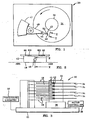
- Disk drive 30 includes a spindle 32 that supports and rotates a magnetic disk 34.
- Spindle 32 is rotated by a motor 36 that, in turn, is controlled by a motor controller 38.
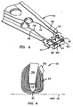
- a horizontal combined magnetic head 40 for reading and recording is mounted on a slider 42.
- Slider 42 is supported by a suspension 44 and actuator arm 46.
- a plurality of disks, sliders and suspensions may be employed in a large capacity direct access storage device (DASD), as shown in FIG. 3 .
- DASD direct access storage device
- Suspension 44 and actuator arm 46 position slider 42 to locate magnetic head 40 in a transducing relationship with a surface of magnetic disk 34.
- slider 42 is supported on a thin (typically, 0.05 ⁇ m) cushion of air (air bearing) between the disk and an air bearing surface (ABS) 48.
- DASD direct access storage device
- Magnetic head 40 may be employed for writing information to multiple circular tracks on the surface of disk 34, as well as for reading information therefrom.
- Processing circuitry 50 exchanges signals representing such information with magnetic head 40, provides motor drive signals, and also provides control signals for moving slider 42 to various tracks.
- slider 42 is shown mounted to a head gimbal assembly (HGA) 52 that is mounted to suspension 44. All of the above components are supported on a base 53.
- HGA head gimbal assembly
- FIG. 5 is a side cross-sectional elevation view of a conventional merged magnetoresistive (MR) head 40 as viewed in plane V ⁇ V of FIG. 2 .
- Magnetic head 40 has a write head portion 54 ("non-pedestal type") and a read head portion 56.
- the read head portion includes an MR sensor 58.
- MR sensor 58 is sandwiched between first and second gap layers 60 and 62 that are, in turn, sandwiched between first and second shield layers 64 and 66.
- the resistance of MR sensor 58 changes.
- a sense current conducted through MR sensor 58 causes these resistance changes to be manifested as potential changes, which are processed by the processing circuitry 50 shown in FIG. 3 .
- Write head portion 54 of the head includes a coil layer 68 sandwiched between first and second insulation layers 70 and 72.
- First and second insulation layers 70 and 72 are referred to as an "insulation stack”.
- Coil layer 68 and first and second insulation layers 70 and 72 are sandwiched between first and second pole pieces 76 and 78.
- First and second pole pieces 76 and 78 are magnetically coupled at a back gap 80, and have first and second pole tips 82 and 84 that are separated by a non-magnetic gap layer 86 at the ABS.
- coil layer 68 is contained completely above non-magnetic gap layer 86 under and within second pole piece 78. As shown in FIGs.
- first and second solder connections 88 and 90 connect leads (not shown) from MR sensor 58 to leads 96 and 98 on suspension 44; third and fourth solder connections 100 and 102 connect leads 104 and 106 from write coil 68 (see FIG. 6 ) to leads 108 and 110 on suspension 44.
- FIG. 8 is a partial cross-sectional view of another conventional slider and magnetic head ("pedestal type") as viewed in plane V--V of FIG. 2 , where the magnetic head may include an MR or a GMR sensor.
- FIG. 9 is a partial ABS view of the slider taken along plane IX-- IX of FIG. 8 to show read and write elements of this magnetic head.
- the head in FIG. 8 includes a pedestal-type write head wherein first pole piece 76 includes a first pole piece layer 80 and a plated pedestal 152. Pedestal 152 is formed on first pole piece layer 80 by electroplating and is made of a magnetic material having a high magnetic moment.
- Non-magnetic gap layer 86 separates pedestal 152 from second pole piece 78. Similar to pedestal 152, a back gap pedestal 154 is formed on first pole piece layer 80 but in the back gap region. A third pole piece 156, which is formed in an arcuate fashion with a front end formed on top of second pole piece 78, serves as a magnetic flux connecting layer.
- Conventional write coils 68 are formed within the magnetic head in a different manner than that in FIG. 5 .
- a first layer of coil turns are formed below non-magnetic gap layer 86 in between pedestals 152 and 154 and a second layer of coil turns are formed above second pole piece 78 within an arcuate spacing formed by third pole piece 156.
- shield layer 66 and first pole piece layer 80 are not common layers; they are separate.
- a non-magnetic separating layer 150 is formed between shield layer 66 and first pole piece layer 80.
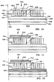
- FIG. 10 a partial cross-sectional view of a magnetic head 1000 in accordance with one embodiment of the present invention is shown.
- a read head portion of magnetic head 1000 includes a GMR sensor 1002 sandwiched in between first and second shield layers 1004 and 1006, being protected within surrounding insulator materials 1008.
- a write head portion of magnetic head 1000 includes a magnetic yoke 1070.
- Magnetic yoke 1070 is the "horseshoe" or similarly shaped magnetic body which has a lower magnetic pole and an upper magnetic pole.
- the lower pole of magnetic yoke 1070 includes a first pole piece layer 1012 and a first pedestal structure 1014 and the upper pole of magnetic yoke 1070 includes a second pole piece 1016 and a third pole piece layer 1028 which serves as a magnetic connecting layer to the back gap region.
- First pedestal structure 1014 includes at least one pedestal, which may be electroplated over first pole piece layer 1012 just behind an air bearing surface (ABS) 1020 of magnetic head 1000.
- first pedestal structure 1014 is a double pedestal structure having an upper pedestal with a magnetic moment that is larger than that of the lower pedestal.
- a non-magnetic write gap layer 1018 separates the pole tips of the lower and the upper poles, being particularly formed between first pedestal structure 1014 and second pole piece 1016.
- Third pole piece layer 1028 has a front end formed partially on top of second pole piece 1016 and a back end formed on top of one or more magnetic connecting pedestals 1017 in the back gap region.
- the one or more magnetic connecting pedestals 1017 are formed on top of first pole piece layer 1012.
- a separation layer 1010 separates second shield layer 1006 from first pole piece layer 1012.
- Magnetic yoke 1070 may be made with any suitable magnetic materials, preferably materials having a high magnetic moment, such as various compositions of NiFe alloys, CoFe alloys, or FeAlN, with the inclusion of other common additives or dopants to control its material properties.
- Write gap layer 1018 and separation layer 1010 may be made of alumina (Al 2 O 3 ) or other suitable non-magnetic or dielectric material.
- magnetic write flux is produced across write gap layer 1018 across the pole tips of magnetic yoke 1070.
- Current is driven through write coils 1022 to generate this magnetic write flux, as is conventional.
- heat is generated by write coils 1022 and thermally transferred to surrounding magnetic head components. If nothing is done to reduce such heating, thermal expansion will undesirably cause outward protrusion of pole tip materials from the ABS 1020 and therefore the fly height of magnetic head 1000 will have to be increased to avoid head-to-disk mechanical interaction.
- write coils 1022 of magnetic head 1000 are formed with a structure that reduces its electrical resistance to thereby reduce heating. This, in turn, reduces or substantially eliminates thermal protrusion at the ABS 1020.
- write coils 1022 are formed with a plurality of coil layers, such as a write coil layer 1024.
- Each coil layer 1024 of write coils 1022 is made with an electrically conductive material, such as copper (Cu). Other materials may be suitable, such as gold, silver, or aluminum.
- a dielectric coil separating layer such as a coil separating layer 1026, which may be made from hard-baked photoresist, alumina (Al 2 O 3 ), silicon-dioxide (SiO 2 ), or other suitable material.
- each coil layer 1024 extends continuously between the lower and upper poles of magnetic yoke 1070.
- One end of each coil layer 1024 is in close proximity to a top of first pole piece layer 1012, being separated only by a thin insulative layer.
- the other end of each coil layer 1024 is in close proximity to a bottom of third pole piece layer 1028 and is also separated by an insulator. It is noted that each coil layer 1024 even extends through a plane 1050 defined by write gap layer 1018 (shown as a dashed line in FIG. 10 ).
- each coil layer 1024 of write coils 1022 is relatively taller in height than those of conventional write coils.
- write coils 1022 utilize a large amount of electrically conductive materials (e.g. copper) as compared to that used in conventional write coils.
- An increase in the volume of conductive materials in write coils 1022 leads to a decrease in the electrical resistance of write coils 1022.
- a reduction in the electrical resistance of write coils 1022 leads to a reduction of heat generation during the write process which, in turn, leads to a reduction in protrusion of magnetic head 1000.
- each coil layer 1024 may be formed between about 2.0 - 7.0 micrometers ( ⁇ m). In the present embodiment, the height of each coil layer 1024 is about 4 ⁇ m. It is noted that, although maximum benefits are provided where each coil layer 1024 extends between magnetic yoke 1070 from top to bottom to the fullest practical extent, sufficient benefits may still be achieved with a reduced height of one or both ends of each coil layer 1024. For example, one or both ends of each coil layer 1024 may extend to have a height that is at least half the height of its corresponding pole pedestal/structure.
- write coils 1022 are provided with six (6) coil turns. However, any suitable number of coil turns may be utilized. For example, write coils 1022 may have between about 1 - 20 coil turns. For lower resistance coils, the width of coil layer 1024 should be maximized while the width of coil separating layer 1026 should be minimized. Using conventional coil fabrication processes, however, each coil separating layer 1026 can only be formed with a width of between 0.4 - 1.0 ⁇ m (nominally, 0.5 ⁇ m for a coil layer of 2 ⁇ m in height).
- coil layer 1024 and coil separating layer 1026 are formed such that each coil separating layer 1026 can be made with a width of between about 0.2 - 0.3 ⁇ m (i.e. less than 0.4 ⁇ m). This can be done using a damascene process. Note that the "coil pitch" is the summation of coil layer 1024 and coil separating layer 1026.
- write coils 1022 have a reduced electrical resistance which is sufficient to reduce thermal protrusion in magnetic head 1000.
- Conventional write coil structures with 6 - 7 coil turns typically have resistances between about 4 - 9 Ohms (i.e. about 0.5 - 1.5 Ohm per coil turn).
- write coils 1022 exhibit a relatively low electrical resistance of about 2 - 4 Ohms.
- this write coil structure provides about 0.3 - 0.5 Ohms per coil turn.
- write coils 1022 of the present invention may exhibit electrical resistances of about 1 - 3 Ohms.
- the structure can provide less than 0.5 Ohms per coil turn and less than 4 Ohms of total electrical resistance.
- Write coils 1022 may be formed in accordance with one of a number of different suitable techniques, conventional or otherwise.
- write coils 1022 are fabricated utilizing a damascene process to achieve a larger coil layer 1024 relative to each coil separating layer 1026.
- materials are formed (e.g. electroplated or vacuum-deposited) within openings previously made by etching (e.g. a reactive ion etch or RIE), and excess material is removed by polishing (e.g. a chemical/mechanical polishing or CMP).
- etching e.g. a reactive ion etch or RIE
- polishing e.g. a chemical/mechanical polishing or CMP
- FIG. 11 is the same magnetic head shown in FIG. 10 except that the upper pole of magnetic yoke 1070 is made with a horizontally laminated structure 1102 of alternating magnetic and non-magnetic dielectric layers. Horizontally laminated structure 1102 may be formed on top of connecting magnetic pedestals 1104 and 1106, which are formed on top of pole pieces 1016 and 1017, respectively.
- FIG. 12 is the same magnetic head shown in FIG. 11 except that the lower pole of magnetic yoke 1070 (i.e. the first pole piece layer) is also made with a horizontally laminated structure 1202 of alternating magnetic and non-magnetic dielectric layers.
- each layer of the horizontally laminated structures 1102 and 1202 may be vacuum-deposited and patterned by ion milling.
- Each magnetic layer may be made of the same magnetic materials previously described for magnetic yoke 1070, and each non-magnetic dielectric layer may be made of a suitable dielectric or non-magnetic material such as Alumina (Al 2 O 3 ) or SiO 2 .
- Each magnetic layer may have a thickness of between about 50 - 2000 Angstroms and each non-magnetic dielectric layer may have a thickness of between about 10 - 200 Angstroms.
- the magnetic head described above includes a magnetic yoke; a write gap layer formed between upper and lower poles of the magnetic yoke; and a write coil having a plurality of coil layers.
- Each coil layer extends continuously between the upper and the lower poles through a plane defined by the write gap layer.
- the write coil is preferably formed using a damascene process, where each coil layer has a larger width relative to each coil separating layer.
- the write coil structure has a reduced electrical resistance for reducing the Joule heating produced in the write coils.
- either one or both of the lower and upper poles may include a horizontally laminated structure of alternating magnetic and non-magnetic dielectric layers to further reduce heating due to core losses originating from eddy current losses. The reduction of heating in the magnetic head leads to reduced protrusion.
- FIG. 13 a partial cross-sectional view of a magnetic head 1300 in accordance with another embodiment of the present invention is shown.
- a read head portion of magnetic head 1300 includes a GMR sensor 1302 sandwiched in between first and second shield layers 1304 and 1306, being protected within surrounding insulator materials 1308.
- a write head portion of magnetic head 1300 includes a magnetic yoke 1370.
- Magnetic yoke 1370 is the "horseshoe" or similarly shaped magnetic body which has a lower magnetic pole and an upper magnetic pole.
- the lower pole of magnetic yoke 1370 includes a first pole piece layer 1312 and a first pedestal structure 1314 and the upper pole of magnetic yoke 1370 includes a second pole piece 1316, a magnetic connecting pedestal 1350, and a third pole piece layer 1328 which serves as a magnetic connecting layer to the back gap region.
- First pedestal structure 1314 includes at least one pedestal, which may be electroplated over first pole piece layer 1312 just behind an air bearing surface (ABS) 1320 of magnetic head 1300.
- a non-magnetic write gap layer 1318 separates the pole tips of the lower and the upper poles, being formed particularly between first pedestal structure 1314 and second pole piece 1316.
- Third pole piece layer 1328 has a front end formed on top of magnetic connecting pedestal 1350, which is formed on top of second pole piece 1316.
- Third pole piece layer 1328 has a back end formed on top of one or more magnetic connecting pedestals 1352 in the back gap region. The one of more magnetic connecting pedestals 1352 are formed on top of first pole piece layer 1312.
- a separation layer 1310 separates second shield layer 1306 from first pole piece layer 1312.
- Magnetic yoke 1370 may be made with any suitable magnetic materials, preferably materials having a high magnetic moment, such as various compositions of NiFe alloys, CoFe alloys, or FeAlN, with the inclusion of other common additives or dopants to control its material properties.
- Write gap layer 1318 and separation layer 1310 may be made of alumina (Al 2 O 3 ) or other suitable non-magnetic or dielectric material.
- magnetic write flux is produced across write gap layer 1318 at the pole tips of magnetic yoke 1370.
- Current is driven through write coils 1322 to generate this magnetic write flux, as is conventional.
- heat is generated by write coils 1322 and thermally transferred to surrounding magnetic head components. If nothing is done to reduce such heating, thermal expansion will undesirably cause outward protrusion of pole tip materials from the ABS 1320 and therefore the fly height will have to be increased to avoid heat-to-disk mechanical interaction.
- write coils 1322 of magnetic head 1300 are formed with a structure that reduces its electrical resistance to thereby reduce heating. This, in turn, reduces or eliminates protrusion of the head elements at the ABS 1320.
- write coils 1322 are formed with a plurality of coil layers, such as a write coil layer 1324.
- Each coil layer 1324 of write coils 1322 is made with a suitable electrically conductive material, such as copper (Cu). Other materials may be suitable, such as gold, silver, and aluminum.
- a suitable electrically conductive material such as copper (Cu).
- Other materials may be suitable, such as gold, silver, and aluminum.
- a coil separating layer 1326 In between each coil layer 1324 is a plurality of dielectric coil separating layers, such as a coil separating layer 1326, which may be made from hard-baked photoresist, alumina (Al 2 O 3 ), silicon-dioxide (SiO 2 ), or other suitable material.
- each coil layer 1324 extends continuously between write gap layer 1318 and the upper pole of magnetic yoke 1370.
- One end of each coil layer 1324 is in close proximity to a top of write gap layer 1318, being separated only by a thin insulative layer.
- the other end of each coil layer 1324 is in close proximity to a bottom of third pole piece layer 1328 and is also separated by an insulator. It is noted that, in this embodiment, no coil layer 1324 extends between the lower pole and write gap layer 1318.
- each coil layer 1324 of write coils 1322 is taller in height than those of conventional write coils.
- Magnetic connecting pedestals 1350 and 1352 help to extend the height of each coil layer 1324.
- write coils 1322 utilize a relatively large amount of electrically conductive materials (e.g. copper) as compared to that used in conventional write coils.
- An increase in the volume of conductive materials in write coils 1322 leads to a decrease in the electrical resistance of write coils 1322.
- a reduction in the electrical resistance of write coils 1322 leads to a reduction of heat generation during the write process which, in turn, leads to a reduction in protrusion of magnetic head 1300.
- each coil layer 1324 may be formed between about 2.0 - 7.0 micrometers ( ⁇ m). In the present embodiment, the height of each coil layer 1324 is about 4 ⁇ m. It is noted that, although maximum benefits are provided where each coil layer 1324 extends between magnetic yoke 1370 from top to bottom to the fullest practical extent, sufficient benefits may be achieved with a reduced height of one or both ends of each coil layer 1324.
- write coils 1322 are provided with six (6) coil turns. However, any suitable number of coil turns may be provided. For example, write coils 1322 may preferably have between about 1 - 20 coil turns. For lower resistance coils, the width of coil layer 1324 should be maximized while the width of coil separating layer 1326 should be minimized. Using conventional coil fabrication processes, however, each coil separating layer 1326 can only be formed with a width of between 0.4 - 1.0 ⁇ m (nominally, 0.5 ⁇ m for a coil layer of 2 ⁇ m in height).
- coil layer 1324 and coil separating layer 1326 are formed such that each coil separating layer 1326 can be made with a width of between about 0.2 - 0.3 ⁇ m (i.e. less than 0.4 ⁇ m). This can be achieved using a damascene process. Note that the "coil pitch" is the summation of coil layer 1324 and coil separating layer 1326.
- write coils 1322 have a reduced electrical resistance which is sufficient to reduce thermal protrusion in magnetic head 1300.
- Conventional write coil structures with 6 - 7 coil turns typically have resistances of between about 4 - 9 Ohms (i.e. about 0.5 - 1.5 Ohm per coil turn).
- write coils 1322 exhibited a relatively low electrical resistance of about 2 - 4 Ohms.
- this write coil structure provides about 0.3 - 0.5 Ohms per coil turn.
- write coils 1322 of the present invention may exhibit electrical resistances of about 1 - 3 Ohms.
- the structure can provide less than 0.5 Ohms per coil turn and less than 4 Ohms of total electrical resistance.
- Write coils 1322 may be formed in accordance with one of a number of different suitable techniques, conventional or otherwise.
- write coils 1322 are fabricated utilizing a damascene process to achieve a larger width of each coil layer 1324 relative to each coil separating layer 1326.
- materials are formed (e.g. electroplated or vacuum-deposited) within openings which are previously formed by etching (e.g. a reactive ion etch or RIE), and excess material is removed by polishing (e.g. a chemical/mechanical polishing or CMP).
- etching e.g. a reactive ion etch or RIE
- polishing e.g. a chemical/mechanical polishing or CMP
- FIG. 14 is the same magnetic head shown in FIG. 13 except that the upper pole of magnetic yoke 1370 is made with a horizontally laminated structure 1402 of alternating magnetic and non-magnetic dielectric layers. Horizontally laminated structure 1402 may be formed on top of magnetic connecting pedestals 1404 and 1406, which are formed on top of magnetic connecting pedestals 1350 and 1352, respectively.
- FIG. 15 is the same magnetic head shown in FIG. 14 except that the lower pole of magnetic yoke 1370 (i.e. the first pole piece layer) is also made with a horizontally laminated structure 1502 of alternating magnetic and non-magnetic dielectric layers.
- each layer of the horizontally laminated structures 1402 and 1502 may be formed by vacuum-deposition and subsequent patterning by ion milling.
- Each magnetic layer may be made of the same magnetic materials previously described for magnetic yoke 1370, and each non-magnetic dielectric layer may be made of a suitable dielectric or non-magnetic material such as Alumina (Al 2 O 3 ) or silicon-dioxide (SiO 2 ).
- Each magnetic layer may have a thickness of between about 50 and 2000 Angstroms and each non-magnetic dielectric layer may have a thickness of between about 10 and 200 Angstroms.
- each horizontally-laminated structure there may be a total of between 4 and 400 layers of magnetic/non-magnetic dielectric materials.
- the top end of each coil layer 1324 may be further extended to be in close/closer proximity to the bottom of horizontally laminated structure 1402.
- FIGs. 13-15 may be preferred over that of FIGs. 10-12 where the spacing between the read sensor and the write gap layer are to be minimized and left independent of the desired height of the write coils.
- write coils 1322 and 1330 of FIGs 13-15 are alternatively positioned in between write gap layer 1318 and the lower pole of magnetic yoke 1370 (e.g. the first pole piece 1312).
- additional magnetic connecting pedestals 1350 and 1352 are not formed in the position shown in FIGs. 13-15 , but rather are formed over first pole piece layer 1312.
- a magnetic head of the present invention may be constructed such that the above-described write coils are positioned in between write gap layer and either the lower pole or the upper pole of the magnetic yoke.
- a magnetic head as described above includes a magnetic yoke; a write gap layer formed between upper and lower poles of the magnetic yoke; and a write coil having a plurality of coil layers.
- Each coil layer extends continuously between the write gap layer and either the lower pole or the upper pole of the magnetic yoke.
- the write coil is preferably formed using a damascene process, where each coil layer is wider than each coil separating layer.
- the write coil structure has a reduced electrical resistance for reducing the Joule heating produced in the write coils.
- either one or both of the lower and upper poles may include a horizontally laminated structure of alternating magnetic and non-magnetic dielectric layers to further reduce heating due to core losses originating from eddy current losses. The reduction of heating in the magnetic head leads to reduced protrusion.
Landscapes
- Engineering & Computer Science (AREA)
- Manufacturing & Machinery (AREA)
- Physics & Mathematics (AREA)
- Electromagnetism (AREA)
- Magnetic Heads (AREA)
Applications Claiming Priority (2)
| Application Number | Priority Date | Filing Date | Title |
|---|---|---|---|
| US629060 | 1984-07-09 | ||
| US10/629,060 US7079353B2 (en) | 2003-07-29 | 2003-07-29 | Magnetic head having a write coil structure with a reduced electrical resistance for reducing thermal protrusion |
Publications (2)
| Publication Number | Publication Date |
|---|---|
| EP1503373A1 EP1503373A1 (en) | 2005-02-02 |
| EP1503373B1 true EP1503373B1 (en) | 2008-12-31 |
Family
ID=33541470
Family Applications (1)
| Application Number | Title | Priority Date | Filing Date |
|---|---|---|---|
| EP04017016A Expired - Lifetime EP1503373B1 (en) | 2003-07-29 | 2004-07-19 | Magnetic head and magnetic recording device |
Country Status (7)
| Country | Link |
|---|---|
| US (2) | US7079353B2 (https=) |
| EP (1) | EP1503373B1 (https=) |
| JP (1) | JP2005050509A (https=) |
| KR (1) | KR20050013956A (https=) |
| CN (1) | CN1291379C (https=) |
| DE (1) | DE602004018715D1 (https=) |
| SG (1) | SG120168A1 (https=) |
Families Citing this family (20)
| Publication number | Priority date | Publication date | Assignee | Title |
|---|---|---|---|---|
| US6947246B2 (en) * | 2003-08-29 | 2005-09-20 | Hitachi Global Storage Technologies Netherlands, B.V. | Large protrusion recording head for controlled magnetic spacing recording/reading |
| US7397625B2 (en) * | 2003-08-29 | 2008-07-08 | Hitachi Global Storage Technologies Netherlands B.V. | Large protrusion recording head for controlled magnetic spacing recording/reading |
| US7272883B2 (en) * | 2003-08-29 | 2007-09-25 | Hitachi Global Storage Technologies Netherlands B.V. | Methods of forming an electrical connection in a magnetic head using a damascene process |
| US7199974B1 (en) * | 2004-02-02 | 2007-04-03 | Western Digital (Fremont), Inc. | Read/write head with reduced pole tip protrusion |
| JP2006120274A (ja) * | 2004-10-25 | 2006-05-11 | Hitachi Global Storage Technologies Netherlands Bv | 薄膜磁気ヘッド |
| JP2006252620A (ja) * | 2005-03-09 | 2006-09-21 | Hitachi Global Storage Technologies Netherlands Bv | 磁気ヘッド及びその製造方法 |
| US7952375B2 (en) * | 2006-06-06 | 2011-05-31 | Formfactor, Inc. | AC coupled parameteric test probe |
| US7633710B2 (en) * | 2006-06-28 | 2009-12-15 | Hitachi Global Storage Technologies B.V. | Magnetic head having reduced induction coil electrical resistance and method for the fabrication thereof |
| US7804662B2 (en) * | 2006-12-26 | 2010-09-28 | Hitachi Global Storage Technologies Netherlands B.V. | Perpendicular magnetic recording head including wrap around shield with notched top write gap and method of fabricating the same |
| US7633711B2 (en) * | 2007-02-07 | 2009-12-15 | Hitachi Global Storage Technologies Netherlands B.V. | Magnetic write head with helical coil structure using multiple materials |
| US7835111B2 (en) * | 2007-02-15 | 2010-11-16 | Hitachi Global Storage Technologies Netherlands B.V. | Magnetic write head with upper return pole optimization for reduced trailing shield protrusion |
| US7440220B1 (en) | 2007-05-29 | 2008-10-21 | Western Digital (Fremont), Llc | Method for defining a touch-down power for head having a flying height actuator |
| US7436620B1 (en) | 2007-05-29 | 2008-10-14 | Western Digital (Fremont), Llc | Method for selecting an electrical power to be applied to a head-based flying height actuator |
| US8066892B2 (en) * | 2008-09-30 | 2011-11-29 | Hitachi Global Storage Technologies Netherlands B.V. | Method for manufacturing a perpendicular magnetic write head with a wrap around shield |
| US20100290157A1 (en) * | 2009-05-14 | 2010-11-18 | Western Digital (Fremont), Llc | Damascene coil processes and structures |
| US8681446B2 (en) | 2011-12-21 | 2014-03-25 | Seagate Technology Llc | Methods and devices including multiple resistive heating elements |
| CN102601097A (zh) * | 2012-03-01 | 2012-07-25 | 浙江工业大学 | 一种分离餐厨废弃物中固体杂质和油脂的装置和方法 |
| US8947807B2 (en) | 2012-12-20 | 2015-02-03 | Seagate Technology Llc | Independently driven write coils |
| US11393776B2 (en) * | 2018-05-17 | 2022-07-19 | Advanced Semiconductor Engineering, Inc. | Semiconductor device package and method of manufacturing the same |
| WO2021258303A1 (zh) * | 2020-06-23 | 2021-12-30 | 庆鼎精密电子(淮安)有限公司 | 相机模组及其制备方法 |
Family Cites Families (19)
| Publication number | Priority date | Publication date | Assignee | Title |
|---|---|---|---|---|
| US174435A (en) * | 1876-03-07 | Improvement in wire-fence-barb formers | ||
| US60879A (en) * | 1867-01-01 | Nicholas gotten | ||
| US5331495A (en) | 1990-06-11 | 1994-07-19 | Fuji Photo Film Co., Ltd. | Thin film magnetic head and methods for producing same |
| US5173826A (en) * | 1991-06-03 | 1992-12-22 | Read-Rite Corp. | Thin film head with coils of varying thickness |
| US6043959A (en) | 1998-03-23 | 2000-03-28 | Read-Rite Corporation | Inductive write head formed with flat yoke and merged with magnetoresistive read transducer |
| US6191918B1 (en) | 1998-10-23 | 2001-02-20 | International Business Machines Corporation | Embedded dual coil planar structure |
| US6226149B1 (en) | 1998-12-15 | 2001-05-01 | International Business Machines Corporation | Planar stitched write head having write coil insulated with inorganic insulation |
| JP2000268321A (ja) | 1999-03-18 | 2000-09-29 | Alps Electric Co Ltd | 薄膜磁気ヘッド |
| US6466402B1 (en) | 1999-06-18 | 2002-10-15 | Read-Rite Corporation | Compact MR write structure |
| US6396660B1 (en) * | 1999-08-23 | 2002-05-28 | Read-Rite Corporation | Magnetic write element having a thermally dissipative structure |
| JP2001076320A (ja) * | 1999-09-02 | 2001-03-23 | Tdk Corp | 薄膜磁気ヘッドおよびその製造方法 |
| US6452742B1 (en) * | 1999-09-02 | 2002-09-17 | Read-Rite Corporation | Thin film write having reduced resistance conductor coil partially recessed within middle coat insulation |
| US7023658B1 (en) * | 2000-02-08 | 2006-04-04 | Western Digital (Fremont), Inc. | Submicron track-width pole-tips for electromagnetic transducers |
| JP2001250203A (ja) | 2000-03-08 | 2001-09-14 | Fujitsu Ltd | 薄膜磁気ヘッドの製造方法 |
| JP2002025006A (ja) | 2000-07-11 | 2002-01-25 | Tdk Corp | 薄膜磁気ヘッド及び薄膜磁気ヘッドの製造方法 |
| JP2002157707A (ja) | 2000-11-21 | 2002-05-31 | Alps Electric Co Ltd | 薄膜磁気ヘッド |
| US7117583B2 (en) | 2002-03-18 | 2006-10-10 | International Business Machines Corporation | Method and apparatus using a pre-patterned seed layer for providing an aligned coil for an inductive head structure |
| US7035046B1 (en) * | 2002-03-19 | 2006-04-25 | Western Digital (Fremont), Inc. | System and method for minimizing thermal pole tip protrusion |
| US6927939B2 (en) * | 2003-01-30 | 2005-08-09 | Headway Technologies, Inc. | Thin-film magnetic head and method of manufacturing same |
-
2003
- 2003-07-29 US US10/629,060 patent/US7079353B2/en not_active Expired - Fee Related
-
2004
- 2004-06-30 SG SG200403776A patent/SG120168A1/en unknown
- 2004-07-19 EP EP04017016A patent/EP1503373B1/en not_active Expired - Lifetime
- 2004-07-19 DE DE602004018715T patent/DE602004018715D1/de not_active Expired - Fee Related
- 2004-07-21 JP JP2004212628A patent/JP2005050509A/ja not_active Withdrawn
- 2004-07-27 KR KR1020040058831A patent/KR20050013956A/ko not_active Ceased
- 2004-07-29 CN CNB200410059033XA patent/CN1291379C/zh not_active Expired - Fee Related
-
2006
- 2006-03-14 US US11/375,160 patent/US7190552B2/en not_active Expired - Fee Related
Also Published As
| Publication number | Publication date |
|---|---|
| US7190552B2 (en) | 2007-03-13 |
| US20060152849A1 (en) | 2006-07-13 |
| KR20050013956A (ko) | 2005-02-05 |
| US7079353B2 (en) | 2006-07-18 |
| SG120168A1 (en) | 2006-03-28 |
| US20050024764A1 (en) | 2005-02-03 |
| CN1577494A (zh) | 2005-02-09 |
| DE602004018715D1 (de) | 2009-02-12 |
| EP1503373A1 (en) | 2005-02-02 |
| CN1291379C (zh) | 2006-12-20 |
| JP2005050509A (ja) | 2005-02-24 |
Similar Documents
| Publication | Publication Date | Title |
|---|---|---|
| EP1503373B1 (en) | Magnetic head and magnetic recording device | |
| US6466404B1 (en) | Magnetic read/write device with insulated coil layer recessed into pole | |
| US7272883B2 (en) | Methods of forming an electrical connection in a magnetic head using a damascene process | |
| US6178070B1 (en) | Magnetic write head and method for making same | |
| US6433968B1 (en) | Merged read/write head and method of fabricating same | |
| US7054113B1 (en) | Reader/writer for magnetic memory | |
| US6466402B1 (en) | Compact MR write structure | |
| US7633711B2 (en) | Magnetic write head with helical coil structure using multiple materials | |
| US7174623B2 (en) | Method of providing protection to the pole piece of a magnetic head during its manufacture with use of a selectively etchable material | |
| KR100469533B1 (ko) | 스핀 밸브 센서의 자기 저항을 증가시키는 산화 니켈 피닝층에 대한 시드층 | |
| US6687085B2 (en) | Perpendicular write head with high magnetization pole material and method of fabricating the write head | |
| JP2003510737A (ja) | 記録ヘッド上のトラック幅を規定するための方法および構造 | |
| JP2002025015A (ja) | 磁気トンネル効果型磁気ヘッド及びその製造方法 | |
| US7593183B2 (en) | Magnetic write head design for reducing temperature induced protrusion | |
| US20150138668A1 (en) | Multi-read sensor having a narrow read gap structure | |
| CN1513169A (zh) | 低温磁轭型隧道阀传感器 | |
| US6972932B2 (en) | High-efficiency single-turn write head for high-speed recording | |
| US6985339B2 (en) | Disc drive having electromagnetic biased shieldless CPP reader | |
| US6989964B2 (en) | Magnetic head having a pole piece with a double pedestal structure | |
| US7275306B2 (en) | Damascene method for forming write coils of magnetic heads | |
| US6842306B2 (en) | Magnetic head having highly thermally conductive insulator materials containing cobalt-oxide | |
| JP2002025014A (ja) | 磁気トンネル効果型磁気ヘッド及び記録再生装置 | |
| JP2002026423A (ja) | 磁気トンネル接合素子の製造方法及び磁気トンネル効果型磁気ヘッドの製造方法 | |
| JPH08153313A (ja) | 磁気抵抗効果型ヘッド及び磁気ディスク装置 | |
| JP2006331570A (ja) | 薄膜磁気ヘッドおよびその製造方法 |
Legal Events
| Date | Code | Title | Description |
|---|---|---|---|
| PUAI | Public reference made under article 153(3) epc to a published international application that has entered the european phase |
Free format text: ORIGINAL CODE: 0009012 |
|
| AK | Designated contracting states |
Kind code of ref document: A1 Designated state(s): AT BE BG CH CY CZ DE DK EE ES FI FR GB GR HU IE IT LI LU MC NL PL PT RO SE SI SK TR |
|
| AX | Request for extension of the european patent |
Extension state: AL HR LT LV MK |
|
| 17P | Request for examination filed |
Effective date: 20050629 |
|
| AKX | Designation fees paid |
Designated state(s): DE FR GB |
|
| 17Q | First examination report despatched |
Effective date: 20060825 |
|
| GRAP | Despatch of communication of intention to grant a patent |
Free format text: ORIGINAL CODE: EPIDOSNIGR1 |
|
| GRAS | Grant fee paid |
Free format text: ORIGINAL CODE: EPIDOSNIGR3 |
|
| GRAA | (expected) grant |
Free format text: ORIGINAL CODE: 0009210 |
|
| AK | Designated contracting states |
Kind code of ref document: B1 Designated state(s): DE FR GB |
|
| REG | Reference to a national code |
Ref country code: GB Ref legal event code: FG4D |
|
| REF | Corresponds to: |
Ref document number: 602004018715 Country of ref document: DE Date of ref document: 20090212 Kind code of ref document: P |
|
| PLBE | No opposition filed within time limit |
Free format text: ORIGINAL CODE: 0009261 |
|
| STAA | Information on the status of an ep patent application or granted ep patent |
Free format text: STATUS: NO OPPOSITION FILED WITHIN TIME LIMIT |
|
| 26N | No opposition filed |
Effective date: 20091001 |
|
| GBPC | Gb: european patent ceased through non-payment of renewal fee |
Effective date: 20090719 |
|
| REG | Reference to a national code |
Ref country code: FR Ref legal event code: ST Effective date: 20100331 |
|
| PG25 | Lapsed in a contracting state [announced via postgrant information from national office to epo] |
Ref country code: FR Free format text: LAPSE BECAUSE OF NON-PAYMENT OF DUE FEES Effective date: 20090731 |
|
| PG25 | Lapsed in a contracting state [announced via postgrant information from national office to epo] |
Ref country code: GB Free format text: LAPSE BECAUSE OF NON-PAYMENT OF DUE FEES Effective date: 20090719 |
|
| PG25 | Lapsed in a contracting state [announced via postgrant information from national office to epo] |
Ref country code: DE Free format text: LAPSE BECAUSE OF NON-PAYMENT OF DUE FEES Effective date: 20100202 |