EP1501202B1 - Antenne interne et un terminal mobile avec l'antenne interne - Google Patents
Antenne interne et un terminal mobile avec l'antenne interne Download PDFInfo
- Publication number
- EP1501202B1 EP1501202B1 EP04016987A EP04016987A EP1501202B1 EP 1501202 B1 EP1501202 B1 EP 1501202B1 EP 04016987 A EP04016987 A EP 04016987A EP 04016987 A EP04016987 A EP 04016987A EP 1501202 B1 EP1501202 B1 EP 1501202B1
- Authority
- EP
- European Patent Office
- Prior art keywords
- terminal
- pcb
- electromagnetic wave
- carrier
- shielding
- Prior art date
- Legal status (The legal status is an assumption and is not a legal conclusion. Google has not performed a legal analysis and makes no representation as to the accuracy of the status listed.)
- Not-in-force
Links
Images


Classifications
-
- H—ELECTRICITY
- H01—ELECTRIC ELEMENTS
- H01Q—ANTENNAS, i.e. RADIO AERIALS
- H01Q1/00—Details of, or arrangements associated with, antennas
- H01Q1/12—Supports; Mounting means
- H01Q1/22—Supports; Mounting means by structural association with other equipment or articles
- H01Q1/24—Supports; Mounting means by structural association with other equipment or articles with receiving set
- H01Q1/241—Supports; Mounting means by structural association with other equipment or articles with receiving set used in mobile communications, e.g. GSM
- H01Q1/242—Supports; Mounting means by structural association with other equipment or articles with receiving set used in mobile communications, e.g. GSM specially adapted for hand-held use
- H01Q1/243—Supports; Mounting means by structural association with other equipment or articles with receiving set used in mobile communications, e.g. GSM specially adapted for hand-held use with built-in antennas
-
- H—ELECTRICITY
- H04—ELECTRIC COMMUNICATION TECHNIQUE
- H04B—TRANSMISSION
- H04B1/00—Details of transmission systems, not covered by a single one of groups H04B3/00 - H04B13/00; Details of transmission systems not characterised by the medium used for transmission
- H04B1/38—Transceivers, i.e. devices in which transmitter and receiver form a structural unit and in which at least one part is used for functions of transmitting and receiving
- H04B1/3827—Portable transceivers
- H04B1/3833—Hand-held transceivers
- H04B1/3838—Arrangements for reducing RF exposure to the user, e.g. by changing the shape of the transceiver while in use
Definitions
- the present invention relates to a mobile terminal having an internal antenna.
- a mobile terminal is a wireless communication device that a user can carry along and make a call while traveling.
- mobile terminals have been fortified in multimedia functions to allow a large amount of information to be transmitted and received.
- performance of an antenna plays a critical role in mobile terminals.
- the antenna of a mobile terminal is installed in the mobile terminal, rather than exposed.
- Such an internal antenna is applied to various fields such as a bluetooth, a wireless LAN, a GSM, a CDMA, or the like, and a local area wireless communication.
- Figure 1 shows a related art mobile terminal.
- the mobile terminal includes a first or main body 8 having various circuit components embedded therein, a menu button 2 and a dial button 4 provided at its front surface and a battery 6 mounted at its rear surface.
- a second body or folder 10 displaying various information using a display 12 or the like can be hinged or the like at the main body 8.
- FIG. 2 is a partial sectional view of the related art mobile terminal.
- the main body 8 of the mobile terminal includes a case 20 having a space therein, a main PCB 22 housed inside the case 20, and an internal antenna 24 separately mounted inside the case 20 and electrically connected to the main PCB 22 to transmit and receive radio waves bearing voice and image information or the like to and from the main PCB 22.
- the internal antenna 24 includes a carrier 30 fixed at an inner side of the case 20, a radiator 32 formed in a certain pattern at a surface of the carrier 30 and radiating radio wave that the main PCB 22 transmits and receives, and a feeding terminal 34 connected to the radiator 32 by wire 36.
- the feeding terminal 34 is electrically connected to an antenna terminal unit 28 of the main PCB 22.
- voice or image information signal generated from the main PCB 22 is radiated from the radiator 32 attached on the carrier 30 through the feeding terminal 34 connected to the antenna terminal unit 28 of the main PCB 22 and the wire 36 connected therebetween. Further, a radio wave signal received through the radiator 32 is transmitted to the main PCB 22 through the wire 36 connected to the radiator 32 and the feeding terminal 34.
- the main body case 20 is injection-molded, and an electromagnetic wave shielding film 40 having a certain thickness is formed as copper and nickel are sequentially plated at an inner side thereof, in order to prevent electromagnetic wave generated from parts 46 attached to the main PCB 22 from being discharged outwardly.
- the related art internal antenna-installed mobile terminal has various disadvantages and problems.
- the carrier 30, which has the radiator 32 for transmitting and receiving voice and image signals attached on its surface is mounted inside the main body case 20 and connected to the main PCB 22 through the wire 36, a space for installing the internal antenna 24 must be secured inside the main body case 20. This results in an increase in size of the main body case 20, and accordingly, the overall size of the terminal is increased.
- Document US 2003/0103014 A1 concerns an antenna and a shield for a communication device.
- an electromagnetic shield, a spacer and an antenna having an antenna feed is provided out of one substantially continuous piece of conductive material.
- Document US 6,342,869 B1 concerns an antenna device comprising an antenna element provided on a surface of a carrier and connected to a shielding can in which one or more analogue RF components are mounted.
- the shielding can is connected to and functionally integrated with the antenna element.
- An object of the invention is to solve at least the above problems and/or disadvantages and to provide at least the advantages described hereinafter.
- An object of the present invention is to provide a mobile terminal having an internal antenna configured to be mounted on a main PCB and methods thereof so that no additional space is needed for installing the internal antenna inside a main body of the terminal.
- Another object of the present invention is to provide a mobile terminal having an internal antenna capable of reducing or preventing leakage of electromagnetic waves by shielding an RF element among parts installed in a main PCB that discharge electromagnetic waves.
- Another object of the present invention is to provide a mobile terminal having an internal antenna configured to be mounted on a main PCB and capable of reducing or preventing leakage of electromagnetic waves by shielding an RF element among parts installed in a main PCB that discharge electromagnetic wave.
- Another object of the present invention is to provide a mobile terminal having a PCB including a first section grouping mounted circuits configured to emit electromagnetic waves.
- Another object of the present invention is to provide a mobile terminal having a PCB including a first section grouping mounted circuits configured to emit electromagnetic waves and a groove in the first section.
- a mobile terminal may include a terminal case, a PCB provided inside the terminal case and having various circuit components mounted thereon and an internal antenna mounted on the PCB and configured to transmit and receive radio waves bearing voice and image information to and from the PCB and shield electromagnetic wave generating parts mounted on the PCB.
- the mobile terminal includes an internal antenna that includes a carrier inside a communication device and configured to shield electromagnetic wave generating parts, a radiator coupled to the carrier and configured to receive and radiate radio waves transmitted to and received from the communication device and a feeding terminal fixed at the carrier and configured to electrically connect the radiator and an antenna terminal part of the communication device.
- a mobile terminal that includes a terminal case, a main PCB inside the terminal case and configured to have various circuit components mounted thereon and an internal antenna directly mounted on the main PCB and configured to receive and transmit radio waves bearing voice and image information to and from the main PCB.
- a method for assembling a mobile terminal that includes providing a terminal case, providing a PCB including various circuit components inside the terminal case and shielding an RF wave generating part mounted on the PCB using the internal antenna.
- PCB printed circuit board
- Figure 5 is a diagram showing an exploded perspective view of a main body of a mobile terminal in accordance with a preferred embodiment of the present invention.
- Figure 6 is a diagram showing a partial sectional view of a main body of the mobile terminal in accordance with a preferred embodiment of the present invention.
- Figure 7 is a diagram showing a perspective view of a carrier of the internal antenna in accordance with a preferred embodiment of the present invention.
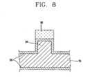
- Figure 8 is a diagram showing a sectional view taken along line VIII-VIII of Figure 7 ;
- Figure 9 is a diagram showing an exploded perspective view of a main body of a mobile terminal in accordance with another preferred embodiment of the present invention.
- Figure 10 is a diagram showing a partially cut perspective view of a main body of the mobile terminal in accordance with another embodiment of the present invention.
- Figure 11 is a diagram showing a perspective view of a carrier of an internal antenna in accordance with another embodiment of the present invention.
- Figure 5 is a diagram showing an exploded perspective view of a main body of a mobile terminal in accordance with one embodiment of the present invention.
- Figure 6 is a diagram showing a partial sectional view of the main body of the mobile terminal of Figure 5 .
- a terminal body 8 having an internal antenna can include cases 50 and 52 enclosing a prescribed space therebetween, a main PCB 54 mounted inside the cases 50 and 52 and having various circuit components mounted thereon and an internal antenna 56 mounted on the main PCB 54.
- the internal antenna 56 can transmit and receive radio waves bearing voice and image information or the like to and from the main PCB 54.
- the case 50 is a front case preferably hinged at a folder 10; and the case 52 is a rear case engaged with the front case 50 to have a certain space therebetween.
- the rear case 52 can include a battery mounting part 60 on which a battery can be mounted.
- the internal antenna 56 can include a carrier 70 fixed at one side of the main PCB 54, a radiator 72 attached at one side of the carrier 70 and radiating radio wave transmitted to and received from the main PCB 54 and a feeding terminal 76 preferably fixed at the carrier 70 and having one end portion connected to the radiator 72 and the other end portion being in contact with an antenna terminal part 74 of the main PCB 54.
- the carrier 70 can include a fixing hole 78 formed at one side, in which the feeding terminal 76 is insertedly fixed, a plurality of engaging hooks 80 formed at a marginal portion thereof and for attaching to the main PCB 54, and screw engaging holes 83 formed at a corner portion thereof so as to be screw-engaged or the like with the front case 50 and the rear case 52.
- an electromagnetic wave shielding part 86 can shield the RF element 82 mounted on the main PCB 54 to thereby reduce or prevent external radiation of electromagnetic wave generated from the RF element 82.
- the carrier 70 can be integrally injection-molded and made of a polycarbonate material or the like.
- the engaging hooks 80 preferably protrude from a marginal portion of the carrier 70 and lock into a hook groove (not shown) formed at the main PCB 54, whereby the carrier 70 is fixed to the main PCB 54.
- the present invention is not intended to be so limited as other fixing devices (e.g., rigidly attached) can be used for coupling the same.
- a connection terminal 90 for electrically coupling the feeding terminal 76 and the radiator 72 is preferably mounted at one side of the fixing hole 78 in which the feeding terminal is insertedly fixed.
- a barrier wall 94 can be formed in a circumferential direction to cover the RF element 82 when the carrier 70 is attached on the main PCB 54. Further, an electromagnetic wave shielding film 96 can be coated at an inner side and an outer side of the electromagnetic wave shielding part 86 to shield electromagnetic wave.
- a gasket 98 is preferably installed at an upper surface of the barrier wall 94 of the electromagnetic wave shielding part 86 being in contact with the surface of the main PCB 54 in order to seal the surface of the main PCB 54 and the electromagnetic wave shielding part 86 to shield electromagnetic wave.
- the electromagnetic wave shielding film 96 can be formed such that a copper film is coated at the surface of the electromagnetic wave shielding part 86 by spraying or vacuum deposition and a corrosion preventing film made of nickel or stainless steel can then be coated at the surface of the copper film by spraying or vacuum deposition.
- the present invention is not intended to be so limited as other materials and processes can be used to form the elctro-magnetic wave shielding film 96 so long as performance criteria are satisfied.
- the gasket 98 is a silicon material having conductivity and elasticity.
- the gasket 98 can be elastically tightly attached at a lower surface of the main PCB 54 to perform an electromagnetic wave shielding function and make an electric grounding.
- an electromagnetic wave shielding film 100 which can be formed by sequentially plating copper and nickel, is preferably coated at an inner side of the front case 50 and the rear case 52 in order to additionally reduce or shield electromagnetic wave generated from parts installed on the main PCB 54.
- the internal antenna 56 In the internal antenna 56, after the feeding terminal 76 is electrically coupled (e.g. fixed) at the carrier 70, the internal antenna 56 is mounted or fixed at one surface (e.g., an upper surface) of the main PCB 54.
- the hook protrusion 80 e.g., formed at the marginal portion of the carrier 70
- the radiator 72 attached to the carrier 70 and the main PCB 54 are electrically coupled.
- the electromagnetic wave shielding part 86 formed at the carrier 70 is tightly attached to the RF element 82 to cover it, thereby shielding electromagnetic waves.
- the front case 50 and the rear case 52 are tightly attached to each other.
- the screw can pass through the screw engaging holes 83 formed at the carrier 70 to engage the carrier 70 together with the front case 50 and the rear case 52.
- the feeding terminal 76 is coupled to the antenna terminal part 74 of the main PCB 54 and the radiator 72 is installed at one side of the carrier 70 for radiating radio wave signal bearing voice and image information generated from the main PCB 54.
- the radio wave signal received through the radiator 72 is received by the antenna terminal part 74 of the main PCB 54 after passing through the feeding terminal 76.
- the RF element 82 of the main PCB 54 is covered by the electromagnetic wave shielding part 86 formed at the carrier 70 and tightly attached to the gasket 98, leakage of electromagnetic wave generated when the RF element 82 operate can be reduced or completely cut off.
- double shielding can be made by the electromagnetic wave shielding film 100 formed at the inner sides of the front case 50 and the rear case 52 around the RF element 82 (e.g., where the electromagnetic wave is mostly generated), and leakage of electromagnetic waves is reduced or prevented by the electromagnetic wave shielding film 100 formed at the front case 50 and the rear case 52 at other remaining regions where the electromagnetic wave is slightly generated (e.g., other components coupled to the main PCB 54). Accordingly, reliable and effective electromagnetic wave shielding can be accomplished.
- Figure 9 is a diagram showing an exploded perspective view of a main body of a mobile terminal in accordance with another embodiment of the present invention.
- Figure 10 is a partially cut perspective view of the main body of the mobile terminal in Figure 9
- Figure 11 is a perspective view of a carrier of an internal antenna in accordance with another embodiment of the present invention.
- FIG. 9 another embodiment of an internal antenna and the mobile terminal housing the same is similar to Figure 5 .
- the embodiment of a carrier 104 of an internal antenna 102 has a different structure.
- the carrier 104 of the internal antenna 102 can include a fixing hole 78 formed at one side thereof, in which the feeding terminal 76 can be insertedly fixed, a plurality of engaging hooks 80 or the like preferably formed at a marginal portion thereof and configured to be fixed to the main PCB 54, and a screw engaging hole 83 or the like preferably formed at a corner portion thereof so as to be screw-engaged with the front case 50 and the rear case 52.
- the front PCB 106 can be a section of the main PCB 54 where electromagnetic wave emitting circuits (e.g., RF element 82) are preferably grouped.
- the first shielding part 110 is preferably formed to cover the RF element at one side of the carrier 104 in order to shield electromagnetic waves generated from the RF element 82, and the second shielding part 112 can be integrally formed at the side of the first shielding part to cover the connector 108 (e.g., FPCB connector) of the front PCB 106.
- the second shielding part 112 can protect the connector 108 and perform an electromagnetic wave shielding operation.
- the connector 108 can be a FPCB connector for connection to a flexible PCB that connects a display module or device (e.g., LCD) in the folder 10 to the main PCB 54.
- the first shielding part 110 and the second shielding part 112 are made of a polycarbonate material.
- the carrier 104, the first shielding part 110 and the second shielding part 112 are integrally injection-molded.
- the present invention is not intended to be so limited as other materials and manufacturing methods can be used.
- a front PCB refuge groove 114 can be formed at the main PCB 54.
- the front PCB refuge groove 114 can allow the front PCB connector 108 to be coupled to an LCD module (e.g., of the folder 10) using a flexible PCB (FPCB).
- the connector 108 of the front PCB 106 can be covered by the second shielding part 112.
- An electromagnetic wave shielding film 96 is preferably coated at an entire surface of the inner side and the outer side of the first shielding part 110 and the second shielding part 112 to shield or reduce electromagnetic waves.
- the electromagnetic wave shielding film 96 can be formed such that a copper film is coated at the surface of the first and second shielding parts 110 and 112 by spraying, vacuum deposition or the like and a corrosion preventing film made of nickel or stainless steel is then coated at the surface of the copper film by spraying, vacuum deposition of the like.
- RF element 82 discharging a large quantity of electromagnetic waves, especially among parts installed on the main PCB 54, and ribs 116 and 118 with a certain height to preferably cover the RF element 82 and the connector 108 of the front PCB 106.
- a gasket 120 can be attached at an upper surface of the ribs 116 and 118 so as to be tightly attached on the surface of the main PCB 54.
- the gasket 120 can be a silicon material having conductivity and elasticity.
- the gasket 98 is elastically tightly attached (e.g., at a lower surface) to the main PCB 54, preferably making an electric grounding.
- embodiments of internal antennas, mobile terminals having an internal antenna and methods for assembling and using the same in accordance with the present invention have various advantages. For example, since an internal antenna can be mounted directly on (e.g., over) the main PCB, a space (e.g., separate from the main PCB) for installation of the antenna is not necessary inside the main body of the terminal. Thus, the terminal can be compact and made smaller. Further, since an electromagnetic wave shielding part for shielding the RF element can be formed in the internal antenna to shield at least one RF element from which a large amount of electromagnetic wave is generated, leakage of electromagnetic wave can be reliably reduced or prevented.
- the electromagnetic wave shielding part can include an electromagnetic wave shielding film on inner and outer surfaces.
- a first shielding part shielding an RF element and the second shield part shielding a front PCB can be formed in an internal antenna
- the RF element generating much electromagnetic wave is double-shielded both by the front PCB shielding part connected to the front PCB and by the electromagnetic wave shielding film formed at an inner side of the casing of the main body.
- electromagnetic waves can be reliably and effectively shielded.
- the internal antenna where the electromagnetic wave shielding member is installed can be simultaneously assembled when the main body casing is assembled, assembly productivity can be enhanced to reduce costs and/or processing time.
Landscapes
- Engineering & Computer Science (AREA)
- Computer Networks & Wireless Communication (AREA)
- Signal Processing (AREA)
- Telephone Set Structure (AREA)
- Shielding Devices Or Components To Electric Or Magnetic Fields (AREA)
- Support Of Aerials (AREA)
Claims (16)
- Terminal mobile, comprenant :un boîtier (50, 52) de terminal ;une carte à circuit imprimé PCB (54) prévue à l'intérieur du boîtier de terminal et ayant divers composants de circuit montés sur celle-ci ; etune antenne interne (56) montée sur la PCB (54) et configurée pour transmettre et recevoir des ondes radio transportant des informations vers et de la PCB (54) et isoler des parties générant des ondes électromagnétiques (82) montées sur la PCB (54),dans lequel l'antenne interne (56) comprend :un support (70) fixé sur un côté de la PCB (54) principale et configuré pour avoir une partie d'isolation d'ondes électromagnétiques (86) ;un radiateur (72) fixé sur le support (70) et configuré pour rayonner lesdites ondes radio reçues de la PCB (54) ; etune broche d'alimentation (76) couplée au support (70) et configurée pour connecter électriquement le radiateur (72) et la PCB (54), caractérisé en ce que le support (70) comprend :une première partie d'isolation (110) configurée pour isoler un élément RF (82) monté sur la PCB (54), etune deuxième partie d'isolation (112) configurée pour isoler un connecteur (108), dans lequel :la première partie d'isolation (110) est configurée pour recouvrir l'élément RF (82) et la deuxième partie d'isolation (112) est configurée pour recouvrir le connecteur (108), etle connecteur (108) est utilisé pour une connexion flexible de la PCB à un clapet du terminal mobile.
- Terminal selon la revendication 1,
dans lequel le support (70) comprend un trou de fixation (78) dans lequel la broche d'alimentation (76) est fixée. - Terminal selon la revendication 1,
dans lequel le support (70) comprend un trou d'engagement (83), dans lequel le trou d'engagement (83) est engagé de façon amovible avec le boîtier (50) de terminal. - Terminal selon la revendication 1,
dans lequel la partie d'isolation d'ondes électromagnétiques (86) recouvre un élément RF (82) monté sur la PCB (54). - Terminal selon la revendication 4, dans lequel la partie d'isolation d'ondes électromagnétiques (86) comprend :une paroi barrière (94) formée dans un sens circonférentiel de manière à ce que l'élément RF (82) puisse être recouvert lorsque le support (70) est fixé sur une surface de la PCB (54) ; etun film d'isolation d'ondes électromagnétiques (96) déposé sur chacun d'un côté intérieur et d'un côté extérieur de la partie d'isolation d'ondes électromagnétiques (86) pour isoler des ondes électromagnétiques.
- Terminal selon la revendication 5,
dans lequel le film d'isolation d'ondes électromagnétiques (96) comprend un film de cuivre sur une surface de la partie d'isolation d'ondes électromagnétiques (86) et un film de prévention de la corrosion incluant du nickel ou de l'acier inoxydable sur une surface du film de cuivre. - Terminal selon la revendication 5,
comprenant un joint statique (98) sur une surface supérieure de la paroi barrière (94) de la partie d'isolation d'ondes électromagnétiques (86) configuré pour sceller la paroi barrière (94) et la surface de la PCB (54). - Terminal selon la revendication 7,
dans lequel le joint statique (98) comprend un matériau de silicone ayant à la fois une conductivité et une élasticité. - Terminal selon la revendication 1, dans lequel le boîtier de terminal comprend :un boîtier avant (50) et un boîtier arrière (52) déterminant un espace prescrit entre ceux-ci ; etun film d'isolation d'ondes électromagnétiques (100) au niveau d'un côté intérieur du boîtier avant (50) et du boîtier arrière (52).
- Terminal selon la revendication 9,
dans lequel le film d'isolation d'ondes électromagnétiques (100) est plaqué séquentiellement de cuivre et de nickel. - Terminal selon la revendication 1,
dans lequel l'antenne interne (56) est par-dessus la PCB (54). - Terminal selon la revendication 1,
dans lequel les première et deuxième parties d'isolation (110, 112) comprennent un matériau de polycarbonate, et dans lequel le support (70), la première partie d'isolation (110) et la deuxième partie d'isolation (112) sont formés de façon intégrale. - Terminal selon la revendication 1,
dans lequel un film d'isolation d'ondes électromagnétiques (100) est déposé sur une surface du côté extérieur et du côté intérieur de chacune des première et deuxième parties d'isolation (110, 112) pour isoler des ondes électromagnétiques. - Terminal selon la revendication 13,
dans lequel le film d'isolation d'ondes électromagnétiques (100) est un film comprenant du cuivre sur la surface des première et deuxième parties d'isolation (110, 112) et un film de prévention de la corrosion incluant du nickel ou de l'acier inoxydable sur la surface du film de cuivre. - Terminal selon la revendication 1,
dans lequel les première et deuxième parties d'isolation (110, 112) incluent respectivement une nervure (116, 118), dans lequel un joint statique (120) est fixé sur une surface supérieure de la nervure et configuré pour être fixé entre la surface de la PCB (54) et la nervure pour isoler des ondes électromagnétiques. - Terminal selon la revendication 1,
dans lequel la PCB (54) comprend une rainure refuge (114) de manière à ce que le connecteur (108) connecté à une PCB avant (106) puisse être recouvert par la deuxième partie d'isolation (112).
Applications Claiming Priority (4)
| Application Number | Priority Date | Filing Date | Title |
|---|---|---|---|
| KR2003050710 | 2003-07-23 | ||
| KR2003050711 | 2003-07-23 | ||
| KR1020030050711A KR100565279B1 (ko) | 2003-07-23 | 2003-07-23 | 전자파 차폐장치 일체형 내장 안테나 및 그 내장안테나를 가지는 휴대용 단말기 |
| KR1020030050710A KR100565278B1 (ko) | 2003-07-23 | 2003-07-23 | 내장 안테나를 가지는 휴대용 단말기 |
Publications (3)
| Publication Number | Publication Date |
|---|---|
| EP1501202A2 EP1501202A2 (fr) | 2005-01-26 |
| EP1501202A3 EP1501202A3 (fr) | 2005-12-14 |
| EP1501202B1 true EP1501202B1 (fr) | 2012-03-28 |
Family
ID=33492560
Family Applications (1)
| Application Number | Title | Priority Date | Filing Date |
|---|---|---|---|
| EP04016987A Not-in-force EP1501202B1 (fr) | 2003-07-23 | 2004-07-19 | Antenne interne et un terminal mobile avec l'antenne interne |
Country Status (5)
| Country | Link |
|---|---|
| US (1) | US7541986B2 (fr) |
| EP (1) | EP1501202B1 (fr) |
| JP (1) | JP4102787B2 (fr) |
| CN (1) | CN100397797C (fr) |
| AT (1) | ATE551780T1 (fr) |
Cited By (1)
| Publication number | Priority date | Publication date | Assignee | Title |
|---|---|---|---|---|
| US9099773B2 (en) | 2006-07-18 | 2015-08-04 | Fractus, S.A. | Multiple-body-configuration multimedia and smartphone multifunction wireless devices |
Families Citing this family (33)
| Publication number | Priority date | Publication date | Assignee | Title |
|---|---|---|---|---|
| US7553295B2 (en) | 2002-06-17 | 2009-06-30 | Iradimed Corporation | Liquid infusion apparatus |
| CN101019335A (zh) * | 2004-08-20 | 2007-08-15 | 皇家飞利浦电子股份有限公司 | 无线终端、无线模块和制造这种终端的方法 |
| US7554494B2 (en) * | 2004-10-21 | 2009-06-30 | Samsung Electronics Co., Ltd. | Built-in antenna module in portable wireless terminal |
| US20060181462A1 (en) * | 2005-02-14 | 2006-08-17 | Intermec Ip Corp. | Integrated antenna/access door for a mobile computer |
| US7627344B2 (en) | 2006-06-07 | 2009-12-01 | Cingular Wireless Ii, Llc | Universal radio module |
| KR101119113B1 (ko) * | 2006-09-29 | 2012-03-16 | 엘지전자 주식회사 | 단말기 |
| US8105282B2 (en) | 2007-07-13 | 2012-01-31 | Iradimed Corporation | System and method for communication with an infusion device |
| US8472203B2 (en) * | 2007-09-04 | 2013-06-25 | Apple Inc. | Assembly of a handheld electronic device |
| CN101453050B (zh) * | 2007-12-07 | 2012-06-27 | 英业达股份有限公司 | 具天线接地结构的电子装置 |
| DE102007062051A1 (de) | 2007-12-21 | 2009-06-25 | Siemens Home And Office Communication Devices Gmbh & Co. Kg | Antennenvorrichtung für funkbasierte elektronische Geräte |
| CN101340470B (zh) * | 2008-08-12 | 2011-04-06 | 苏州佳世达电通有限公司 | 无线通讯装置 |
| US8957813B2 (en) | 2009-03-13 | 2015-02-17 | Pong Research Corporation | External case for redistribution of RF radiation away from wireless communication device user and wireless communication device incorporating RF radiation redistribution elements |
| US9172134B2 (en) | 2008-11-06 | 2015-10-27 | Antenna79, Inc. | Protective cover for a wireless device |
| US8208980B2 (en) | 2008-11-06 | 2012-06-26 | Pong Research Corporation | Radiation redirecting external case for portable communication device and antenna embedded in battery of portable communication device |
| US8214003B2 (en) * | 2009-03-13 | 2012-07-03 | Pong Research Corporation | RF radiation redirection away from portable communication device user |
| KR101127101B1 (ko) * | 2009-02-10 | 2012-03-23 | 제일모직주식회사 | 기구물 일체형 루프 안테나 및 그 제조방법 |
| KR101164098B1 (ko) | 2009-07-14 | 2012-07-12 | (주)블루버드 소프트 | 모바일 단말기 |
| KR101025794B1 (ko) * | 2009-07-14 | 2011-04-04 | (주)블루버드 소프트 | 모바일 단말기 |
| US9838060B2 (en) | 2011-11-02 | 2017-12-05 | Antenna79, Inc. | Protective cover for a wireless device |
| TWI487478B (zh) * | 2012-07-13 | 2015-06-01 | Apone Technology Ltd | 形成金屬構件於機殼的方法 |
| JP5788069B1 (ja) * | 2014-08-29 | 2015-09-30 | 古河電気工業株式会社 | 平面型ヒートパイプ |
| KR20160092875A (ko) * | 2015-01-28 | 2016-08-05 | 삼성전기주식회사 | 안테나 패턴이 매립되는 방사체 프레임 및 이를 포함하는 전자장치 |
| KR102594574B1 (ko) | 2016-01-12 | 2023-10-26 | 삼성전자주식회사 | Rf 케이블 연결장치 및 이를 가지는 전자 장치 |
| CN107124733A (zh) * | 2016-02-24 | 2017-09-01 | 中兴通讯股份有限公司 | 馈线面板及馈线连接方法 |
| KR102527317B1 (ko) * | 2016-08-30 | 2023-05-03 | 삼성전자주식회사 | 금속 패드가 부착된 금속 케이스를 구비한 전자기기 |
| WO2018101112A1 (fr) * | 2016-11-30 | 2018-06-07 | 株式会社村田製作所 | Tableau de connexions, module coupleur et dispositif de communication |
| CN106856524A (zh) * | 2016-12-03 | 2017-06-16 | 胡佳培 | 一种旋转手机 |
| KR102209123B1 (ko) | 2017-12-19 | 2021-01-28 | 삼성전자 주식회사 | 안테나와 rf 소자를 포함하는 모듈 및 이를 포함하는 기지국 |
| US11268506B2 (en) | 2017-12-22 | 2022-03-08 | Iradimed Corporation | Fluid pumps for use in MRI environment |
| JP7171455B2 (ja) * | 2019-01-21 | 2022-11-15 | Dynabook株式会社 | 電子機器 |
| US11146301B2 (en) * | 2019-05-09 | 2021-10-12 | William James Scott | Systems and methods for a cellular phone enclosure |
| FR3098810B1 (fr) * | 2019-07-18 | 2021-10-15 | Commissariat Energie Atomique | Liaison mécanique pour dispositif MEMS et NEMS de mesure d'une variation de pression et dispositif comprenant une telle liaison mécanique |
| WO2024009500A1 (fr) * | 2022-07-08 | 2024-01-11 | 日立Astemo株式会社 | Dispositif de commande électronique et procédé de fabrication de dispositif de commande électronique |
Family Cites Families (27)
| Publication number | Priority date | Publication date | Assignee | Title |
|---|---|---|---|---|
| JP2514979B2 (ja) | 1987-08-28 | 1996-07-10 | 株式会社東芝 | 電子機器のシ−ルド構造 |
| FI85794C (fi) * | 1989-07-05 | 1992-05-25 | Nokia Mobira Oy | Foerfarande foer att skydda ett kretskort eller en del daerav mot stoerningar som alstrats av elektromagnetisk interferens, och skyddshoelje foer anvaendning i foerfarandet. |
| US5436802A (en) * | 1994-03-16 | 1995-07-25 | Motorola | Method and apparatus for shielding an electrical circuit that is disposed on a substrate |
| JPH0870195A (ja) | 1994-08-29 | 1996-03-12 | Japan Radio Co Ltd | プリント回路基板のシールド方法 |
| SG70987A1 (en) * | 1995-05-09 | 2000-03-21 | Motorola Inc | Method and apparatus for routing conductors |
| JP2898603B2 (ja) | 1996-07-02 | 1999-06-02 | 三菱電機株式会社 | 回路基板用シールド機構 |
| JPH10150285A (ja) | 1996-11-20 | 1998-06-02 | Mitsubishi Electric Corp | 電子回路のシールド装置 |
| US6353443B1 (en) | 1998-07-09 | 2002-03-05 | Telefonaktiebolaget Lm Ericsson (Publ) | Miniature printed spiral antenna for mobile terminals |
| SE9904256D0 (sv) | 1999-02-10 | 1999-11-24 | Allgon Ab | An antenna device and a radio communication device including an antenna device |
| US6200142B1 (en) * | 1999-02-22 | 2001-03-13 | Berg Technology, Inc. | Assembly including a flex circuit and a gas tight chamber |
| US6157546A (en) * | 1999-03-26 | 2000-12-05 | Ericsson Inc. | Shielding apparatus for electronic devices |
| JP2000286584A (ja) | 1999-03-30 | 2000-10-13 | Kokusai Electric Co Ltd | 携帯型通信機のシールド構造 |
| US6285324B1 (en) * | 1999-09-15 | 2001-09-04 | Lucent Technologies Inc. | Antenna package for a wireless communications device |
| WO2001028305A1 (fr) * | 1999-10-12 | 2001-04-19 | Shielding For Electronics, Inc. | Appareil de confinement des interferences electromagnetiques |
| JP2001111321A (ja) | 1999-10-13 | 2001-04-20 | Sony Corp | アンテナ装置及び通信端末装置 |
| SE522419C2 (sv) | 1999-10-29 | 2004-02-10 | Ericsson Telefon Ab L M | Modulantenn |
| AU2071701A (en) | 1999-12-10 | 2001-06-18 | Thermion Systems International | A thermoplastic laminate fabric heater and methods for making same |
| US6990355B2 (en) * | 2000-06-30 | 2006-01-24 | Sanyo Electric Co., Ltd. | Flexible printed circuit board and foldable cell phone terminal |
| JP3959945B2 (ja) | 2000-10-02 | 2007-08-15 | 松下電器産業株式会社 | アンテナ付き高周波モジュール |
| JP2002281135A (ja) * | 2001-03-21 | 2002-09-27 | Nec Viewtechnology Ltd | 携帯電話 |
| US6486837B2 (en) * | 2001-04-09 | 2002-11-26 | Molex Incorporated | Antenna structures |
| JP4304358B2 (ja) | 2001-04-20 | 2009-07-29 | 日本電気株式会社 | 携帯電話装置 |
| US20030103014A1 (en) | 2001-12-04 | 2003-06-05 | Thomas Birnbaum | Antenna and shield |
| WO2003094289A1 (fr) * | 2002-05-02 | 2003-11-13 | Sony Ericsson Mobile Communications Ab | Antenne incorporee a circuits imprimes destinee a un appareil de communication electronique portable |
| US6867746B2 (en) * | 2002-06-03 | 2005-03-15 | Kaga Electronics Co., Ltd. | Combined EMI shielding and internal antenna for mobile products |
| KR100488012B1 (ko) * | 2002-11-11 | 2005-05-06 | 엘지전자 주식회사 | 휴대용 컴퓨터 시스템 |
| US7236065B2 (en) * | 2004-04-28 | 2007-06-26 | Nokia Corporation | Integrated RF-front end having an adjustable antenna |
-
2004
- 2004-07-19 EP EP04016987A patent/EP1501202B1/fr not_active Not-in-force
- 2004-07-19 AT AT04016987T patent/ATE551780T1/de active
- 2004-07-22 US US10/896,059 patent/US7541986B2/en not_active Expired - Fee Related
- 2004-07-22 JP JP2004214990A patent/JP4102787B2/ja not_active Expired - Fee Related
- 2004-07-23 CN CNB2004100545762A patent/CN100397797C/zh not_active Expired - Fee Related
Cited By (1)
| Publication number | Priority date | Publication date | Assignee | Title |
|---|---|---|---|---|
| US9099773B2 (en) | 2006-07-18 | 2015-08-04 | Fractus, S.A. | Multiple-body-configuration multimedia and smartphone multifunction wireless devices |
Also Published As
| Publication number | Publication date |
|---|---|
| ATE551780T1 (de) | 2012-04-15 |
| CN100397797C (zh) | 2008-06-25 |
| US7541986B2 (en) | 2009-06-02 |
| JP4102787B2 (ja) | 2008-06-18 |
| EP1501202A3 (fr) | 2005-12-14 |
| US20050017910A1 (en) | 2005-01-27 |
| JP2005045810A (ja) | 2005-02-17 |
| EP1501202A2 (fr) | 2005-01-26 |
| CN1578173A (zh) | 2005-02-09 |
Similar Documents
| Publication | Publication Date | Title |
|---|---|---|
| EP1501202B1 (fr) | Antenne interne et un terminal mobile avec l'antenne interne | |
| US6285327B1 (en) | Parasitic element for a substrate antenna | |
| US7668575B2 (en) | System and method for obtaining radiation characteristics of built-in antenna in mobile communication terminal | |
| US8174452B2 (en) | Cavity antenna for wireless electronic devices | |
| US6563042B2 (en) | Radiating enclosure | |
| US6215454B1 (en) | Multi-layered shielded substrate antenna | |
| US6097339A (en) | Substrate antenna | |
| JP3798733B2 (ja) | 無線モジュールとこの無線モジュールを備えた無線通信端末 | |
| EP1633015B1 (fr) | Elément d'étanchéité et dispositif d'étanchéité pour unité de circuit électronique | |
| JP2002064601A (ja) | 移動電話装置及びその内蔵アンテナ | |
| KR101037898B1 (ko) | 무선 데이터 전송을 채택한 디바이스용 전자파 적합성 장치 | |
| EP1093675B1 (fr) | Antenne de substrat comportant un element de prevention de couplage d'energie entre antenne et conducteurs | |
| CN110622493B (zh) | 通信设备和用于组装通信设备的方法 | |
| KR100738265B1 (ko) | 기판 안테나 | |
| KR100565279B1 (ko) | 전자파 차폐장치 일체형 내장 안테나 및 그 내장안테나를 가지는 휴대용 단말기 | |
| JP4814804B2 (ja) | 移動体無線通信機 | |
| CN108539389B (zh) | 中框、移动终端及中框的制作方法 | |
| JPH11312998A (ja) | 携帯無線機 | |
| KR100565278B1 (ko) | 내장 안테나를 가지는 휴대용 단말기 | |
| KR101240844B1 (ko) | 내장 안테나를 갖는 셋톱 박스 | |
| JP2005020766A (ja) | 携帯無線機 | |
| CN112886212B (zh) | 穿戴式电子设备 | |
| KR200253156Y1 (ko) | 이동통신 단말기의 안테나 | |
| JP2002141724A (ja) | アンテナの取付構造 |
Legal Events
| Date | Code | Title | Description |
|---|---|---|---|
| PUAI | Public reference made under article 153(3) epc to a published international application that has entered the european phase |
Free format text: ORIGINAL CODE: 0009012 |
|
| 17P | Request for examination filed |
Effective date: 20040719 |
|
| AK | Designated contracting states |
Kind code of ref document: A2 Designated state(s): AT BE BG CH CY CZ DE DK EE ES FI FR GB GR HU IE IT LI LU MC NL PL PT RO SE SI SK TR |
|
| AX | Request for extension of the european patent |
Extension state: AL HR LT LV MK |
|
| RIC1 | Information provided on ipc code assigned before grant |
Ipc: 7H 04M 1/02 B Ipc: 7H 01Q 1/52 B Ipc: 7H 04B 1/38 A |
|
| PUAL | Search report despatched |
Free format text: ORIGINAL CODE: 0009013 |
|
| AK | Designated contracting states |
Kind code of ref document: A3 Designated state(s): AT BE BG CH CY CZ DE DK EE ES FI FR GB GR HU IE IT LI LU MC NL PL PT RO SE SI SK TR |
|
| AX | Request for extension of the european patent |
Extension state: AL HR LT LV MK |
|
| AKX | Designation fees paid |
Designated state(s): AT BE BG CH CY CZ DE DK EE ES FI FR GB GR HU IE IT LI LU MC NL PL PT RO SE SI SK TR |
|
| 17Q | First examination report despatched |
Effective date: 20070703 |
|
| RAP1 | Party data changed (applicant data changed or rights of an application transferred) |
Owner name: LG ELECTRONICS, INC. |
|
| RAP1 | Party data changed (applicant data changed or rights of an application transferred) |
Owner name: LG ELECTRONICS, INC. |
|
| GRAP | Despatch of communication of intention to grant a patent |
Free format text: ORIGINAL CODE: EPIDOSNIGR1 |
|
| GRAS | Grant fee paid |
Free format text: ORIGINAL CODE: EPIDOSNIGR3 |
|
| GRAA | (expected) grant |
Free format text: ORIGINAL CODE: 0009210 |
|
| AK | Designated contracting states |
Kind code of ref document: B1 Designated state(s): AT BE BG CH CY CZ DE DK EE ES FI FR GB GR HU IE IT LI LU MC NL PL PT RO SE SI SK TR |
|
| REG | Reference to a national code |
Ref country code: GB Ref legal event code: FG4D |
|
| REG | Reference to a national code |
Ref country code: CH Ref legal event code: EP |
|
| REG | Reference to a national code |
Ref country code: AT Ref legal event code: REF Ref document number: 551780 Country of ref document: AT Kind code of ref document: T Effective date: 20120415 |
|
| REG | Reference to a national code |
Ref country code: IE Ref legal event code: FG4D |
|
| REG | Reference to a national code |
Ref country code: DE Ref legal event code: R096 Ref document number: 602004037077 Country of ref document: DE Effective date: 20120524 |
|
| REG | Reference to a national code |
Ref country code: NL Ref legal event code: VDEP Effective date: 20120328 |
|
| PG25 | Lapsed in a contracting state [announced via postgrant information from national office to epo] |
Ref country code: FI Free format text: LAPSE BECAUSE OF FAILURE TO SUBMIT A TRANSLATION OF THE DESCRIPTION OR TO PAY THE FEE WITHIN THE PRESCRIBED TIME-LIMIT Effective date: 20120328 Ref country code: GR Free format text: LAPSE BECAUSE OF FAILURE TO SUBMIT A TRANSLATION OF THE DESCRIPTION OR TO PAY THE FEE WITHIN THE PRESCRIBED TIME-LIMIT Effective date: 20120629 |
|
| REG | Reference to a national code |
Ref country code: AT Ref legal event code: MK05 Ref document number: 551780 Country of ref document: AT Kind code of ref document: T Effective date: 20120328 |
|
| PG25 | Lapsed in a contracting state [announced via postgrant information from national office to epo] |
Ref country code: CY Free format text: LAPSE BECAUSE OF FAILURE TO SUBMIT A TRANSLATION OF THE DESCRIPTION OR TO PAY THE FEE WITHIN THE PRESCRIBED TIME-LIMIT Effective date: 20120328 |
|
| PG25 | Lapsed in a contracting state [announced via postgrant information from national office to epo] |
Ref country code: EE Free format text: LAPSE BECAUSE OF FAILURE TO SUBMIT A TRANSLATION OF THE DESCRIPTION OR TO PAY THE FEE WITHIN THE PRESCRIBED TIME-LIMIT Effective date: 20120328 Ref country code: SE Free format text: LAPSE BECAUSE OF FAILURE TO SUBMIT A TRANSLATION OF THE DESCRIPTION OR TO PAY THE FEE WITHIN THE PRESCRIBED TIME-LIMIT Effective date: 20120328 Ref country code: CZ Free format text: LAPSE BECAUSE OF FAILURE TO SUBMIT A TRANSLATION OF THE DESCRIPTION OR TO PAY THE FEE WITHIN THE PRESCRIBED TIME-LIMIT Effective date: 20120328 Ref country code: SI Free format text: LAPSE BECAUSE OF FAILURE TO SUBMIT A TRANSLATION OF THE DESCRIPTION OR TO PAY THE FEE WITHIN THE PRESCRIBED TIME-LIMIT Effective date: 20120328 Ref country code: RO Free format text: LAPSE BECAUSE OF FAILURE TO SUBMIT A TRANSLATION OF THE DESCRIPTION OR TO PAY THE FEE WITHIN THE PRESCRIBED TIME-LIMIT Effective date: 20120328 Ref country code: PL Free format text: LAPSE BECAUSE OF FAILURE TO SUBMIT A TRANSLATION OF THE DESCRIPTION OR TO PAY THE FEE WITHIN THE PRESCRIBED TIME-LIMIT Effective date: 20120328 Ref country code: BE Free format text: LAPSE BECAUSE OF FAILURE TO SUBMIT A TRANSLATION OF THE DESCRIPTION OR TO PAY THE FEE WITHIN THE PRESCRIBED TIME-LIMIT Effective date: 20120328 |
|
| PG25 | Lapsed in a contracting state [announced via postgrant information from national office to epo] |
Ref country code: PT Free format text: LAPSE BECAUSE OF FAILURE TO SUBMIT A TRANSLATION OF THE DESCRIPTION OR TO PAY THE FEE WITHIN THE PRESCRIBED TIME-LIMIT Effective date: 20120730 Ref country code: SK Free format text: LAPSE BECAUSE OF FAILURE TO SUBMIT A TRANSLATION OF THE DESCRIPTION OR TO PAY THE FEE WITHIN THE PRESCRIBED TIME-LIMIT Effective date: 20120328 |
|
| PG25 | Lapsed in a contracting state [announced via postgrant information from national office to epo] |
Ref country code: DK Free format text: LAPSE BECAUSE OF FAILURE TO SUBMIT A TRANSLATION OF THE DESCRIPTION OR TO PAY THE FEE WITHIN THE PRESCRIBED TIME-LIMIT Effective date: 20120328 Ref country code: NL Free format text: LAPSE BECAUSE OF FAILURE TO SUBMIT A TRANSLATION OF THE DESCRIPTION OR TO PAY THE FEE WITHIN THE PRESCRIBED TIME-LIMIT Effective date: 20120328 Ref country code: AT Free format text: LAPSE BECAUSE OF FAILURE TO SUBMIT A TRANSLATION OF THE DESCRIPTION OR TO PAY THE FEE WITHIN THE PRESCRIBED TIME-LIMIT Effective date: 20120328 |
|
| PLBE | No opposition filed within time limit |
Free format text: ORIGINAL CODE: 0009261 |
|
| STAA | Information on the status of an ep patent application or granted ep patent |
Free format text: STATUS: NO OPPOSITION FILED WITHIN TIME LIMIT |
|
| PG25 | Lapsed in a contracting state [announced via postgrant information from national office to epo] |
Ref country code: MC Free format text: LAPSE BECAUSE OF NON-PAYMENT OF DUE FEES Effective date: 20120731 |
|
| REG | Reference to a national code |
Ref country code: CH Ref legal event code: PL |
|
| 26N | No opposition filed |
Effective date: 20130103 |
|
| REG | Reference to a national code |
Ref country code: DE Ref legal event code: R097 Ref document number: 602004037077 Country of ref document: DE Effective date: 20130103 |
|
| PG25 | Lapsed in a contracting state [announced via postgrant information from national office to epo] |
Ref country code: LI Free format text: LAPSE BECAUSE OF NON-PAYMENT OF DUE FEES Effective date: 20120731 Ref country code: CH Free format text: LAPSE BECAUSE OF NON-PAYMENT OF DUE FEES Effective date: 20120731 |
|
| REG | Reference to a national code |
Ref country code: IE Ref legal event code: MM4A |
|
| PG25 | Lapsed in a contracting state [announced via postgrant information from national office to epo] |
Ref country code: BG Free format text: LAPSE BECAUSE OF FAILURE TO SUBMIT A TRANSLATION OF THE DESCRIPTION OR TO PAY THE FEE WITHIN THE PRESCRIBED TIME-LIMIT Effective date: 20120628 Ref country code: IE Free format text: LAPSE BECAUSE OF NON-PAYMENT OF DUE FEES Effective date: 20120719 |
|
| PG25 | Lapsed in a contracting state [announced via postgrant information from national office to epo] |
Ref country code: ES Free format text: LAPSE BECAUSE OF FAILURE TO SUBMIT A TRANSLATION OF THE DESCRIPTION OR TO PAY THE FEE WITHIN THE PRESCRIBED TIME-LIMIT Effective date: 20120709 |
|
| PG25 | Lapsed in a contracting state [announced via postgrant information from national office to epo] |
Ref country code: TR Free format text: LAPSE BECAUSE OF FAILURE TO SUBMIT A TRANSLATION OF THE DESCRIPTION OR TO PAY THE FEE WITHIN THE PRESCRIBED TIME-LIMIT Effective date: 20120328 |
|
| PG25 | Lapsed in a contracting state [announced via postgrant information from national office to epo] |
Ref country code: LU Free format text: LAPSE BECAUSE OF NON-PAYMENT OF DUE FEES Effective date: 20120719 |
|
| PG25 | Lapsed in a contracting state [announced via postgrant information from national office to epo] |
Ref country code: HU Free format text: LAPSE BECAUSE OF FAILURE TO SUBMIT A TRANSLATION OF THE DESCRIPTION OR TO PAY THE FEE WITHIN THE PRESCRIBED TIME-LIMIT Effective date: 20040719 |
|
| REG | Reference to a national code |
Ref country code: FR Ref legal event code: PLFP Year of fee payment: 12 |
|
| PGFP | Annual fee paid to national office [announced via postgrant information from national office to epo] |
Ref country code: GB Payment date: 20150615 Year of fee payment: 12 |
|
| PGFP | Annual fee paid to national office [announced via postgrant information from national office to epo] |
Ref country code: FR Payment date: 20150612 Year of fee payment: 12 |
|
| PGFP | Annual fee paid to national office [announced via postgrant information from national office to epo] |
Ref country code: DE Payment date: 20150612 Year of fee payment: 12 |
|
| PGFP | Annual fee paid to national office [announced via postgrant information from national office to epo] |
Ref country code: IT Payment date: 20150710 Year of fee payment: 12 |
|
| REG | Reference to a national code |
Ref country code: DE Ref legal event code: R119 Ref document number: 602004037077 Country of ref document: DE |
|
| GBPC | Gb: european patent ceased through non-payment of renewal fee |
Effective date: 20160719 |
|
| PG25 | Lapsed in a contracting state [announced via postgrant information from national office to epo] |
Ref country code: FR Free format text: LAPSE BECAUSE OF NON-PAYMENT OF DUE FEES Effective date: 20160801 Ref country code: DE Free format text: LAPSE BECAUSE OF NON-PAYMENT OF DUE FEES Effective date: 20170201 |
|
| REG | Reference to a national code |
Ref country code: FR Ref legal event code: ST Effective date: 20170331 |
|
| PG25 | Lapsed in a contracting state [announced via postgrant information from national office to epo] |
Ref country code: GB Free format text: LAPSE BECAUSE OF NON-PAYMENT OF DUE FEES Effective date: 20160719 |
|
| PG25 | Lapsed in a contracting state [announced via postgrant information from national office to epo] |
Ref country code: IT Free format text: LAPSE BECAUSE OF NON-PAYMENT OF DUE FEES Effective date: 20160719 |